EP1387251B1 - Instruction de copiage de données d'un stockage de piles - Google Patents
Instruction de copiage de données d'un stockage de piles Download PDFInfo
- Publication number
- EP1387251B1 EP1387251B1 EP03291912.8A EP03291912A EP1387251B1 EP 1387251 B1 EP1387251 B1 EP 1387251B1 EP 03291912 A EP03291912 A EP 03291912A EP 1387251 B1 EP1387251 B1 EP 1387251B1
- Authority
- EP
- European Patent Office
- Prior art keywords
- stack
- data
- entry
- micro
- main
- Prior art date
- Legal status (The legal status is an assumption and is not a legal conclusion. Google has not performed a legal analysis and makes no representation as to the accuracy of the status listed.)
- Expired - Lifetime
Links
Images


Classifications
-
- G—PHYSICS
- G06—COMPUTING OR CALCULATING; COUNTING
- G06F—ELECTRIC DIGITAL DATA PROCESSING
- G06F9/00—Arrangements for program control, e.g. control units
- G06F9/06—Arrangements for program control, e.g. control units using stored programs, i.e. using an internal store of processing equipment to receive or retain programs
- G06F9/30—Arrangements for executing machine instructions, e.g. instruction decode
- G06F9/30098—Register arrangements
- G06F9/3012—Organisation of register space, e.g. banked or distributed register file
- G06F9/30134—Register stacks; shift registers
-
- G—PHYSICS
- G06—COMPUTING OR CALCULATING; COUNTING
- G06F—ELECTRIC DIGITAL DATA PROCESSING
- G06F12/00—Accessing, addressing or allocating within memory systems or architectures
- G06F12/02—Addressing or allocation; Relocation
- G06F12/0223—User address space allocation, e.g. contiguous or non contiguous base addressing
- G06F12/023—Free address space management
- G06F12/0253—Garbage collection, i.e. reclamation of unreferenced memory
-
- G—PHYSICS
- G06—COMPUTING OR CALCULATING; COUNTING
- G06F—ELECTRIC DIGITAL DATA PROCESSING
- G06F12/00—Accessing, addressing or allocating within memory systems or architectures
- G06F12/02—Addressing or allocation; Relocation
- G06F12/08—Addressing or allocation; Relocation in hierarchically structured memory systems, e.g. virtual memory systems
- G06F12/0802—Addressing of a memory level in which the access to the desired data or data block requires associative addressing means, e.g. caches
- G06F12/0804—Addressing of a memory level in which the access to the desired data or data block requires associative addressing means, e.g. caches with main memory updating
-
- G—PHYSICS
- G06—COMPUTING OR CALCULATING; COUNTING
- G06F—ELECTRIC DIGITAL DATA PROCESSING
- G06F12/00—Accessing, addressing or allocating within memory systems or architectures
- G06F12/02—Addressing or allocation; Relocation
- G06F12/08—Addressing or allocation; Relocation in hierarchically structured memory systems, e.g. virtual memory systems
- G06F12/0802—Addressing of a memory level in which the access to the desired data or data block requires associative addressing means, e.g. caches
- G06F12/0891—Addressing of a memory level in which the access to the desired data or data block requires associative addressing means, e.g. caches using clearing, invalidating or resetting means
-
- G—PHYSICS
- G06—COMPUTING OR CALCULATING; COUNTING
- G06F—ELECTRIC DIGITAL DATA PROCESSING
- G06F12/00—Accessing, addressing or allocating within memory systems or architectures
- G06F12/02—Addressing or allocation; Relocation
- G06F12/08—Addressing or allocation; Relocation in hierarchically structured memory systems, e.g. virtual memory systems
- G06F12/12—Replacement control
- G06F12/121—Replacement control using replacement algorithms
- G06F12/126—Replacement control using replacement algorithms with special data handling, e.g. priority of data or instructions, handling errors or pinning
-
- G—PHYSICS
- G06—COMPUTING OR CALCULATING; COUNTING
- G06F—ELECTRIC DIGITAL DATA PROCESSING
- G06F9/00—Arrangements for program control, e.g. control units
- G06F9/06—Arrangements for program control, e.g. control units using stored programs, i.e. using an internal store of processing equipment to receive or retain programs
- G06F9/30—Arrangements for executing machine instructions, e.g. instruction decode
- G06F9/30098—Register arrangements
- G06F9/30101—Special purpose registers
-
- G—PHYSICS
- G06—COMPUTING OR CALCULATING; COUNTING
- G06F—ELECTRIC DIGITAL DATA PROCESSING
- G06F9/00—Arrangements for program control, e.g. control units
- G06F9/06—Arrangements for program control, e.g. control units using stored programs, i.e. using an internal store of processing equipment to receive or retain programs
- G06F9/30—Arrangements for executing machine instructions, e.g. instruction decode
- G06F9/3017—Runtime instruction translation, e.g. macros
- G06F9/30174—Runtime instruction translation, e.g. macros for non-native instruction set, e.g. Javabyte, legacy code
-
- G—PHYSICS
- G06—COMPUTING OR CALCULATING; COUNTING
- G06F—ELECTRIC DIGITAL DATA PROCESSING
- G06F2212/00—Indexing scheme relating to accessing, addressing or allocation within memory systems or architectures
- G06F2212/50—Control mechanisms for virtual memory, cache or TLB
- G06F2212/502—Control mechanisms for virtual memory, cache or TLB using adaptive policy
Definitions
- the present invention relates generally to synchronizing stack storage that may be located external to a processor's core to stack storage that may be located internal to a processor's core.
- multimedia functionality may include, without limitation, games, audio decoders, digital cameras, etc. It is thus desirable to implement such functionality in an electronic device in a way that, all else being equal, is fast, consumes as little power as possible and requires as little memory as possible. Improvements in this area are desirable.
- the present invention resides in a system and a method for implementing a multi-stack processor as set forth in the appended claims.
- the system comprises a main stack, a local data stack and plurality of flags.
- the main stack comprises a plurality of entries and is located outside a processor's core, while the local data stack is coupled to the main stack and is located internal to the processor's core.
- the local data stack has a plurality of entries that correspond to entries in the main stack. Each flag is associated with a corresponding entry in the local data stack and indicates whether the data in the corresponding local data stack entry is valid.
- the system preferably performs two instructions. One of the instructions copies all valid data from the local data stack in the processor's core to corresponding entries in the main stack outside the processor's core and invalidates all previously valid local data stack entries. The other instruction copies all valid data from the local data stack to the main stack, but does not invalidate the local data stack.
- Other embodiments comprise related methods.
- system is used to refer to a collection of components.
- a system may comprise a processor and memory and other components.
- a system also may comprise a collection of components internal to a single processor and, as such, a processor may be referred to as a system.
- the subject matter disclosed herein is directed to a programmable electronic device such as a processor.
- the processor described herein is particularly suited for executing JavaTM bytecodes or comparable, code.
- Java is particularly suited for embedded applications.
- Java is a relatively "dense" language meaning that on average each instruction may perform a large number of functions compared to various other programming languages.
- the dense nature of Java is of particular benefit for portable, battery-operated devices that preferably include as little memory as possible to save space and power. The reason, however, for executing Java code is not material to this disclosure or the claims that follow.
- the processor described herein may be used in a wide variety of electronic systems.
- the Java-executing processor described herein may be used in a portable, battery-operated cell phone.
- the processor advantageously includes one or more features that reduce the amount of power consumed by the Java-executing processor.
- System 100 includes at least two processors 102 and 104.
- Processor 102 is referred to for purposes of this disclosure as a Java Stack Machine ("JSM") and processor 104 may be referred to as a Main Processor Unit (“MPU").
- System 100 may also include an external memory 106 coupled to both the JSM 102 and MPU 104 and thus accessible by both processors.
- the external memory 106 may exist on a separate chip than the JSM 102 and the MPU 104. At least a portion of the external memory 106 may be shared by both processors meaning that both processors may access the same shared memory locations.
- System 100 also includes a Java Virtual Machine (“JVM”) 108, compiler 110, and a display 114.
- the JSM 102 preferably includes an interface to one or more input/output (“I/O") devices such as a keypad to permit a user to control various aspects of the system 100.
- I/O input/output
- data streams may be received from the I/O space into the JSM 102 to be processed by the JSM 102.
- Other components may include, without limitation, a battery and an analog transceiver to permit wireless communications with other devices.
- system 100 may be representative of, or adapted to, a wide variety of electronic systems, an exemplary electronic system may comprise a battery-operated, mobile cell phone.
- Java code comprises a plurality of "bytecodes" 112.
- Bytecodes 112 may be provided to the JVM 108, compiled by compiler 110 and provided to the JSM 102 and/or MPU 104 for execution therein.
- the JSM 102 may execute at least some, and generally most, of the Java bytecodes.
- the JSM 102 may request the MPU 104 to execute one or more Java bytecodes not executed or executable by the JSM 102.
- the MPU 104 also may execute non-Java instructions.
- the MPU 104 also hosts an operating system ("O/S") (not specifically shown), which performs various functions including system memory management, the system task management that schedules the JVM 108 and most or all other native tasks running on the system, management of the display 114, receiving input from input devices, etc.
- O/S operating system
- Java code may be used to perform any one of a variety of applications including multimedia, games or web based applications in the system 100, while non-Java code, which may comprise the O/S and other native applications, may still run on the system on the MPU 104.
- the JVM 108 generally comprises a combination of software and hardware.
- the software may include the compiler 110 and the hardware may include the JSM 102.
- the JSM 102 may execute at least two instruction sets.
- Java bytecode is a stack-based intermediate language in which instructions generally target a stack. For example, an integer add (“IADD") Java instruction pops two integers off the top of the stack, adds them together, and pushes the sum back on the stack.
- IADD integer add
- the JSM 102 comprises a stack-based architecture with various features that accelerate the execution of stack-based Java code, where the stack may include multiple portions that exist in different physical locations.
- Another instruction set executed by the JSM 102 may include instructions other than standard Java instructions.
- other instruction sets may include register-based and memory-based operations to be performed.
- This other instruction set generally complements the Java instruction set and, accordingly, may be referred to as a complementary instruction set architecture ("C-ISA").
- C-ISA complementary instruction set architecture
- a micro-sequence also may include one or more bytecode instructions.
- the execution of Java may be made more efficient and run faster by replacing some sequences of bytecodes by preferably shorter and more efficient sequences of C-ISA instructions.
- the two sets of instructions may be used in a complementary fashion to obtain satisfactory code density and efficiency.
- the JSM 102 generally comprises a stack-based architecture for efficient and accelerated execution of Java bytecodes combined with a register-based architecture for executing register and memory based C-ISA instructions. Both architectures preferably are tightly combined and integrated through the C-ISA.
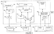
- FIG. 2 shows an exemplary block diagram of the JSM 102.
- the JSM includes a core 120 coupled to a data storage 122 and an instruction storage 130.
- Storage 122 and 130 are preferably integrated, along with core 120, on the same JSM chip. Integrating storage 122 and 130 on the same chip as the core 120 may reduce data transfer time from storage 122 and 130 to the core 120.
- the core 120 may include one or more components as shown.
- Such components preferably include a plurality of registers 140, three address generation units (“AGUs”) 142, 147, micro-translation lookaside buffers (micro-TLBs) 144, 156, a multi-entry micro-stack 146, an arithmetic logic unit (“ALU”) 148, a multiplier 150, decode logic 152, and instruction fetch logic 154.
- ALU arithmetic logic unit
- operands may be retrieved from a main stack and processed by the ALU 148, where the main stack may include multiple portions that exist in different physical locations.
- the main stack may reside in external memory 106 and/or data storage 122. Selected entries from the main stack may exist on the micro-stack 146.
- selected entries on the micro-stack 146 may represent the most current version of the operands in the system 100. Accordingly, operands in external memory 106 and data storage 122 may not be coherent with the versions contained on the micro-stack 146.
- a plurality of flags 158 are associated with the micro-stack 146. Each micro-stack entry preferably has an associated flag 158. Each flag 158 indicates whether the data in the associated micro-stack entry is valid and whether the data has been modified. Also, stack coherency operations may be performed by examining the flags 158 and updating the main stack with valid operands from the micro-stack 146 as will be explained below.
- the micro-stack 146 preferably comprises, at most, the top n entries of the main stack that is implemented in data storage 122 and/or external memory 106.
- the micro-stack 146 preferably comprises a plurality of gates in the core 120 of the JSM 102.
- gates e.g., registers
- access to the data contained on the micro-stack 146 is generally quite fast. Therefore, data access time may be reduced by providing data from the micro-stack 146 instead of the main stack.
- General stack requests are provided by the micro-stack 146 unless the micro-stack 146 cannot fulfill the stack requests.
- n represents the size of the micro-stack 146
- the value of n may be optimized such that a majority of general stack requests are fulfilled by the micro-stack 146, and therefore may provide requested data in fewer cycles.
- power consumption of the system 102 may be reduced.
- the value of n may vary in different embodiments, in accordance with at least some embodiments, the value of n may be the top eight entries in the main stack.
- the micro-stack 146 In this manner, about 98% of the general stack accesses may be provided by the micro-stack 146, and the number of accesses to the main stack may be reduced. As will be seen below, the main stack may not always be coherent with the micro-stack and, there may be a need, at times, to synchronize the main stack to the micro-stack.
- Instructions may be fetched from instruction storage 130 by fetch logic 154 and decoded by decode logic 152.
- the address generation unit 142 may be used to calculate addresses based, at least in part on data contained in the registers 140.
- the AGUs 142 may calculate addresses for C-ISA instructions.
- the AGUs 142 may support parallel data accesses for C-ISA instructions that perform array or other types of processing.
- AGU 147 couples to the micro-stack 146 and may manage overflow and underflow conditions on the micro-stack 146 preferably in parallel.
- the micro-TLBs 144, 156 generally perform the function of a cache for the address translation and memory protection information bits that are preferably under the control of the operating system running on the MPU 104.
- the registers 140 may include 16 registers designated as R0-R15.
- Registers R0-R3, R5, R8-R11 and R13-R14 may be used as general purposes ("GP") registers usable for any purpose by the programmer.
- Other registers, and some of the GP registers, may be used for specific functions.
- registers R4 and R12 may be used to store two program counters.
- Register R4 preferably is used to store the program counter (“PC") and register R12 preferably is used to store a micro-program counter ("micro-PC").
- register R5 may be used to store the base address of a portion of memory in which Java local variables may be stored when used by the current Java method.
- the top of the micro-stack 146 is reflected in registers R6 and R7.
- the top of the micro-stack 146 has a matching address in external memory 106 pointed to by register R6.
- the operands contained on the micro-stack 146 are the latest updated values, while their corresponding values in external memory 106 may or may not be up to date.
- Register R7 provides the data value stored at the top of the micro-stack 146.
- Registers R8 and R9 may also be used to hold an address index 0 ("AI0") and an address index 1 ("AI1"), which may be used in calculating addresses in memory generated by various bytecodes, for example, the result of an IADD instruction.
- Register R14 may also be used to hold the indirect register index ("IRI") that also may be used in calculating memory addresses.
- Register R15 may be used for status and control of the JSM 102.
- one status/control bit (called the "Micro-Sequence-Active” bit) may indicate if the JSM 102 is executing a "simple” instruction or a "complex” instruction through a micro-sequence as explained above. This bit controls in particular, which program counter is used R4 (PC) or R12 (micro-PC) to fetch the next instruction.
- PC program counter
- R12 micro-PC
- a "simple" bytecode instruction is generally one in which the JSM 102 may perform an immediate operation either in a single cycle (e.g., an IADD instruction) or in several cycles (e.g., "dup2_x2").
- a “complex” bytecode instruction is one in which several memory accesses may be required to be made within the JVM data structure for various verifications (e.g., NULL pointer, array boundaries). Because these data structures are generally JVM-dependent and thus may change from one JVM implementation to another, the software flexibility of the micro-sequence provides a mechanism for various JVM optimizations now known or later developed.
- the ALU 148 adds, subtracts, and shifts data.
- the multiplier 150 may be used to multiply two values together in one or more cycles.
- the instruction fetch logic 154 generally fetches instructions from instruction storage 130.
- the instructions may be decoded by decode logic 152. Because the JSM 102 is adapted to process instructions from at least two instruction sets, the decode logic 152 generally comprises at least two modes of operation, one mode for each instruction set. As such, the decode logic unit 152 may include a Java mode in which Java instructions may be decoded and a C-ISA mode in which C-ISA instructions may be decoded.
- the data storage 122 generally comprises data cache ("D-cache”) 124 and data random access memory (“D-RAM”) 126.
- D-cache data cache
- D-RAM data random access memory
- the main stack, arrays and noncritical data may be stored in the D-cache 124, while Java local variables, critical data and non-Java variables (e.g., C, C++) may be stored in D-RAM 126.
- the instruction storage 130 may comprise instruction RAM (“I-RAM”) 132 and instruction cache ("I-cache”) 134.
- the I-RAM 132 may be used for "complex" micro-sequenced bytecodes or micro-sequences or predetermined sequences of code, as will be described below.
- the I-cache 134 may be used to store other types of Java bytecode and mixed Java/C-ISA instructions.
- the C-ISA instructions generally complement the standard Java bytecodes.
- the compiler 110 may scan a series of Java bytes codes 112 and replace one or more of such bytecodes with an optimized code segment mixing C-ISA and bytecodes and which is capable of more efficiently performing the function(s) performed by the initial group of Java bytecodes. In at least this way, Java execution may be accelerated by the JSM 102.
- the JSM 102 implements a split stack architecture.
- the main stack that may be implemented in data storage 122 and/or external memory 106
- each micro-stack entry has a corresponding flag 158.
- the flag 158 indicates whether or not the corresponding micro-stack entry contains valid data.
- a flag 158 designated as "EN” signifies that the flag is enabled indicating that the corresponding micro-stack entry contains valid data.
- a flag that is blank indicates that the corresponding micro-stack entry does not contain valid data (i.e., contains invalid data).
- the micro-stack 146 includes a finite number of entries, and therefore overflow and underflow conditions may occur.
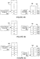
- Figures 4A-C depict an overflow condition of the micro-stack 146. Note that although the micro-stack 146 shown in Figures 4A-C is shown containing four entries, preferred embodiments may have any number of entries.
- the micro-stack 146 may include data values or operands A and B, for example as the result of pushing A and B on the micro-stack 146.
- Stack pointers 162 and 164 reflect the top of the micro-stack 146 and the top of the main stack 160, respectively.
- the flags 158 may be enabled ("EN") to indicate that the new data is valid.
- Operands pushed on the micro-stack 146 generally are not pushed on a main stack 160.
- Operands A' and B' indicate the place of the data in the main stack, but these entries are not coherent with the corresponding micro-stack entries A and B.
- the symbol ( ⁇ ) indicates that the associated operand is not actually present in the main stack. Coherence may be achieved if A and B are written to main memory during an overflow condition or flushing, as explained below.
- the main stack pointer 164 is updated at every push or pop.
- the main stack 160 may exist in external memory 106 and/or data storage 122, and the main stack 160 may be larger than the micro-stack 146.
- Figure 4B shows operands C and D pushed on the micro-stack 146, where the micro-stack 146 is now full. Any subsequent operand is pushed on the micro-stack 146 in a cyclical manner such that when the micro-stack 146 is full, the data at the bottom of the micro-stack 146 (which in this example is operand A) is overwritten. As operands are pushed into entries of the micro-stack 146, the flag 158 associated with each entry may be checked for validity.
- FIG. 4C depicts the result of pushing operand E on the full micro-stack 146 from Figure 4B .
- the bottom of the micro-stack 146 (operand A) is moved into the main stack 160 at an address value equal to the main stack pointer 164 minus the number of entries n comprising the micro-stack 146.
- Figure 4B shows the micro-stack 146 including 4 entries and the main stack pointer 164 indicating the top of the main stack 160.
- operand A is copied to an address that is four entries less than the address indicated by the stack pointer 164.
- operand A from the micro-stack 164 is written to the main stack as indicated in Figure 4C .
- operand E can be written to the micro-stack 146 as shown.
- Figures 5A-C depict an underflow condition of the micro-stack 146 shown in Figure 4C .
- operand E is popped off the micro-stack 146 and then operand D is popped off the micro-stack 146.
- the corresponding flag 158 is invalidated and the stack pointers 162 and 164 are decremented.
- Figure 5B illustrates a bytecode that provides operands B and C to the ALU 148.
- the ALU 148 produces a result Z, which is placed back on the micro-stack 146, and the flag 158 is enabled as shown.
- Flag 158 preferably is checked for valid data prior to executing bytecodes to determine whether the required data is present on the micro-stack 146.
- Figure 5C depicts a bytecode requiring operand Z in addition to operand A, which is not on the micro-stack 146. Since flag 158 associated with operand A is not enabled in Figure 5B , operand A is fetched from the main stack 160. In some embodiments, multiple operands may be fetched simultaneously from the main stack 160. In addition, other embodiments include pre-fetching the operands from the main stack 160.
- Flags 158 may be implemented as one or more registers with bits allocated for each entry in the micro-stack 146, or alternatively flags 158 may include a read pointer and a write pointer.
- the read pointer is preferably updated on each stack instruction execution. For example, during an IADD instruction, the read pointer may decrement itself once for each operand that is popped off the stack, and then increment itself once to write the result of the operand back on the stack.
- the write pointer is preferably updated during an underflow or an overflow. By comparing the values of the read pointer and the write pointer, overflow and underflow conditions can be detected.
- the data in the main stack 160 may not be coherent with data in the micro-stack.
- the micro-stack contains operands B, C, and D that are not present in the main stack.
- the main stack 160 contains operand E that is not present in the micro-stack.
- Situations may occur in which it is desirable to have the main stack 160 contain a complete view of all of the data in the main and micro-stacks and thus be made coherent with the micro-stack. For example, it may be desirable or required to change the current context of the system and doing so may require all stack data to be saved to external storage.
- Performing this action may require all of the stack data to be contained in the main stack to facilitate copying to external storage.
- the preferred embodiments of the invention permit the JSM 102 to execute a "clean and invalidate" instruction to make the main stack coherent with the micro-stack and invalidate the contents of the micro-stack so that, for instance, another thread may use the entire micro-stack.
- the JSM 102 also may execute a "clean" instruction which makes the main stack coherent with the micro-stack, but does not invalidate the data in the micro-stack so that any valid micro-stack data can be readily used as desired.
- a "clean" instruction which makes the main stack coherent with the micro-stack, but does not invalidate the data in the micro-stack so that any valid micro-stack data can be readily used as desired.
- Figure 6 illustrates the operation of the clean and invalidate instruction.
- the state of the micro-stack 146 and the main stack 160 in Figure 6 is repeated from that of Figure 4C .
- the micro-stack 146 is full with valid data for operands B-E and the main stack has valid data for operand A and placeholders for operands B-E.
- micro-stack 146 has valid data that is not present in the main stack 160.
- the clean and invalidate instruction preferably scrolls through some or all of the micro-stack 146, beginning with the top of the micro-stack that is identified by micro-stack pointer 162, and copies all valid data to corresponding entries in the main stack 160 and clears the corresponding valid bits (flags 158) in the micro-stack.
- the order in which the micro-stack entries are examined for valid data to be copied to the main stack is not important and thus the entries can be examined in any order.
- the clean and invalidate instruction causes the JSM 102 to begin with the top of the micro-stack (although other orders are possible) which contains operand E.
- the flag 158 associated with operand E is examined to determine whether the entry contains valid data. In the example of Figure 6 , operand E's flag 158 indicates that operand E is valid.
- the JSM 102 then copies or moves operand E to the top of the main stack identified by pointer 164. Both pointers preferably may be decremented, with the micro-stack pointer 162 being decremented in a cyclical manner. In some embodiments, the pointers 162 and 164 may be saved so as not to lose the current state of the pointers.
- the pointer values may be restored, if desired.
- the pointer 162 After decrementing the micro-stack pointer 162, the pointer 162 then points to the entry containing operand D. Operand D's flag 158 is checked and the JSM determines that operand D is valid. Operand D then is copied or moved to the location pointed to by main stack pointer 164. This process repeats until a micro-stack entry is encountered whose flag 158 indicates that the entry does not contain valid data. In the example of Figure 6 , all micro-stack entries contain valid data, but in other cases, one or more entries may not contain valid data.
- the JSM may change all flags 158 to the invalid state.
- the main stack 160 contains a complete view of all valid stack data. Further processing on one or more stack values may occur as desired.
- the state of the micro-stack 146 at this point is that the micro-stack does not contain any valid data.
- the clean instruction copies valid data from the micro-stack 146 to the main stack.
- the copying process preferably functions as described above with regard to the clean and invalidate instruction.
- the JSM 102 does not change the flags 158 to invalidate any of the micro-stack entries.
- the clean instruction advantageously makes the main stack 160 coherent in the external memory, but still keeps the top values locally in the micro-stack 146, and marked as valid, for later use.
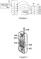
- system 100 may be implemented as a mobile cell phone such as that shown in Figure 7 .
- a mobile communication device includes an integrated keypad 412 and display 414.
- the JSM 102 and MPU 104 and other components may be included in electronics package 410 connected to the keypad 412, display 414, and radio frequency ("RF") circuitry 416.
- the RF circuitry 416 may be connected to an antenna 418.
Landscapes
- Engineering & Computer Science (AREA)
- Theoretical Computer Science (AREA)
- Physics & Mathematics (AREA)
- General Engineering & Computer Science (AREA)
- General Physics & Mathematics (AREA)
- Software Systems (AREA)
- Executing Machine-Instructions (AREA)
Claims (11)
- Système (100), comportant :une pile principale (160) comprenant une pluralité d'entrées et résidant à l'extérieur du coeur (120) d'un processeur, chacune des entrées de la pile principale étant configurable pour contenir des données ;une pile (146) de données locales couplée à la pile principale (160) et située intérieurement au coeur (120) du processeur, la pile (146) de données locales comprenant une pluralité d'entrées qui correspondent à des entrées dans la pile principale (160), et chaque entrée de la pile de données locales étant configurée pour contenir des données ; etune pluralité de fanions (158), chaque fanion étant associé à une entrée correspondante dans la pile (146) de données locales et indiquant si les données dans l'entrée correspondante de la pile de données locales sont valides ;caractérisé en ce que le système exécute une instruction qui copie toutes les données valides de la pile (146) de données locales dans le coeur (120) du processeur vers des entrées correspondantes dans la pile principale (160) à l'extérieur du coeur (120) du processeur.
- Système selon la revendication 1, ledit système examinant le fanion (158) associé à une entrée de la pile de données locales pour déterminer si l'entrée contient des données valides et, seulement si l'entrée contient des données valides, le système copiant les données de l'entrée vers une entrée correspondante dans la pile principale (160).
- Système selon la revendication 1 ou la revendication 2, comprenant en outre un pointeur (162) de pile de données locales associé à la pile (146) de données locales et un pointeur (164) de pile principale associé à la pile principale (160), l'instruction faisant en sorte que le système examine le fanion (158) associé à l'entrée identifiée par le pointeur (162) de pile de données locales pour déterminer si l'entrée en question contient des données valides, et si l'entrée contient des données valides, l'instruction faisant en sorte que le système copie les données de l'entrée vers l'entrée de la pile principale (160) identifiée par le pointeur (164) de pile principale.
- Système selon la revendication 3, le pointeur (162) de pile de données locales étant décrémenté de façon répétée pour permettre aux fanions associés à des entrées supplémentaires de la pile (146) de données locales d'être examinés pour déterminer la validité des données, les données contenues dans chaque entrée dont le fanion (158) indique que les données sont valides étant copiées vers la pile principale (160) au niveau d'une entrée vers laquelle pointe le pointeur (164) de pile principale, le pointeur (164) de pile principale étant également décrémenté.
- Système selon l'une quelconque des revendications précédentes, l'instruction faisant en sorte que le système repositionne un fanion (158) associé à des données valides qui sont copiées vers la pile principale (160) vers un état servant à indiquer que l'entrée ne contient pas de données valides.
- Système selon l'une quelconque des revendications précédentes, l'instruction conservant toutes les données précédemment valides dans la pile (146) de données locales dans la pile (146) de données locales et marquées comme valides par l'intermédiaire des fanions (158) correspondants.
- Procédé, comportant les étapes consistant :en réaction à la réception d'une instruction prédéterminée provenant d'un processeur (102), à examiner un fanion (158) associé à chaque entrée dans une pile (146) de données locales résidant dans le coeur (120) du processeur, le fanion indiquant si l'entrée associée contient des données valides ; etsi le fanion (158) indique la présence de données valides, copier les données de chaque entrée vers une entrée correspondante dans une pile principale (160) qui réside à l'extérieur du coeur (120) du processeur.
- Procédé selon la revendication 7, comportant en outre les étapes consistant à répéter l'examen du fanion (158) et à copier d'éventuelles données valides jusqu'à ce que les fanions (158) associés à toutes les entrées de la pile (146) de données locales comportant des données valides aient été examinés.
- Procédé selon la revendication 7 ou la revendication 8, comportant en outre le repositionnement du fanion (158) pour indiquer que l'entrée associée ne contient pas de données valides.
- Procédé selon la revendication 7, la revendication 8 ou la revendication 9, comportant en outre le non-repositionnement du fanion (158) pour indiquer que l'entrée associée ne contient pas de données valides.
- Procédé selon l'une quelconque des revendications 8 à 10, la copie des données comportant la copie de données d'une entrée de la pile de données locales identifiée par un pointeur (162) de pile de données locales vers une entrée correspondante de la pile principale (160) identifiée par un pointeur (164) de pile principale.
Priority Applications (2)
| Application Number | Priority Date | Filing Date | Title |
|---|---|---|---|
| EP03291912.8A EP1387251B1 (fr) | 2002-07-31 | 2003-07-30 | Instruction de copiage de données d'un stockage de piles |
| US10/631,422 US7162586B2 (en) | 2002-07-31 | 2003-07-31 | Synchronizing stack storage |
Applications Claiming Priority (3)
| Application Number | Priority Date | Filing Date | Title |
|---|---|---|---|
| US40039102P | 2002-07-31 | 2002-07-31 | |
| US400391P | 2002-07-31 | ||
| EP03291912.8A EP1387251B1 (fr) | 2002-07-31 | 2003-07-30 | Instruction de copiage de données d'un stockage de piles |
Publications (3)
| Publication Number | Publication Date |
|---|---|
| EP1387251A2 EP1387251A2 (fr) | 2004-02-04 |
| EP1387251A3 EP1387251A3 (fr) | 2008-01-02 |
| EP1387251B1 true EP1387251B1 (fr) | 2017-09-06 |
Family
ID=38606006
Family Applications (1)
| Application Number | Title | Priority Date | Filing Date |
|---|---|---|---|
| EP03291912.8A Expired - Lifetime EP1387251B1 (fr) | 2002-07-31 | 2003-07-30 | Instruction de copiage de données d'un stockage de piles |
Country Status (2)
| Country | Link |
|---|---|
| US (1) | US7162586B2 (fr) |
| EP (1) | EP1387251B1 (fr) |
Families Citing this family (4)
| Publication number | Priority date | Publication date | Assignee | Title |
|---|---|---|---|---|
| RU2320001C1 (ru) * | 2006-06-23 | 2008-03-20 | Военно-космическая академия имени А.Ф. Можайского | Устройство приоритетного обслуживания запросов |
| US7991962B2 (en) * | 2007-12-10 | 2011-08-02 | International Business Machines Corporation | System and method of using threads and thread-local storage |
| US9274919B2 (en) * | 2011-04-29 | 2016-03-01 | Dynatrace Software Gmbh | Transaction tracing mechanism of distributed heterogenous transactions having instrumented byte code with constant memory consumption and independent of instrumented method call depth |
| GB2622286A (en) * | 2022-09-02 | 2024-03-13 | Advanced Risc Mach Ltd | Synchronization of load/store operations |
Family Cites Families (15)
| Publication number | Priority date | Publication date | Assignee | Title |
|---|---|---|---|---|
| US5107457A (en) * | 1989-04-03 | 1992-04-21 | The Johns Hopkins University | Stack data cache having a stack management hardware with internal and external stack pointers and buffers for handling underflow and overflow stack |
| US5893148A (en) * | 1994-03-03 | 1999-04-06 | International Business Machines Corporation | System and method for allocating cache memory storage space |
| US6604190B1 (en) * | 1995-06-07 | 2003-08-05 | Advanced Micro Devices, Inc. | Data address prediction structure and a method for operating the same |
| US5970242A (en) * | 1996-01-24 | 1999-10-19 | Sun Microsystems, Inc. | Replicating code to eliminate a level of indirection during execution of an object oriented computer program |
| US5953741A (en) * | 1996-11-27 | 1999-09-14 | Vlsi Technology, Inc. | Stack cache for stack-based processor and method thereof |
| US6122711A (en) * | 1997-01-07 | 2000-09-19 | Unisys Corporation | Method of and apparatus for store-in second level cache flush |
| US6098089A (en) | 1997-04-23 | 2000-08-01 | Sun Microsystems, Inc. | Generation isolation system and method for garbage collection |
| US6092152A (en) * | 1997-06-23 | 2000-07-18 | Sun Microsystems, Inc. | Method for stack-caching method frames |
| US6219757B1 (en) * | 1998-02-27 | 2001-04-17 | Sun Microsystems, Inc. | Cache flush operation for a stack-based microprocessor |
| US6219783B1 (en) * | 1998-04-21 | 2001-04-17 | Idea Corporation | Method and apparatus for executing a flush RS instruction to synchronize a register stack with instructions executed by a processor |
| GB9907283D0 (en) | 1999-03-31 | 1999-05-26 | Koninkl Philips Electronics Nv | Memory reclamation method |
| EP1182565B1 (fr) | 2000-08-21 | 2012-09-05 | Texas Instruments France | Antémémoire et DMA à bit de validité global |
| EP1182562B1 (fr) | 2000-08-21 | 2011-05-11 | Texas Instruments France | Antémémoire intelligente à préextraction de bloc interruptible |
| US6567905B2 (en) | 2001-01-23 | 2003-05-20 | Gemstone Systems, Inc. | Generational garbage collector with persistent object cache |
| EP1304620A1 (fr) | 2001-10-17 | 2003-04-23 | Texas Instruments Incorporated | Antémémoire avec attribution sélective d'écriture |
-
2003
- 2003-07-30 EP EP03291912.8A patent/EP1387251B1/fr not_active Expired - Lifetime
- 2003-07-31 US US10/631,422 patent/US7162586B2/en not_active Expired - Lifetime
Non-Patent Citations (1)
| Title |
|---|
| None * |
Also Published As
| Publication number | Publication date |
|---|---|
| EP1387251A3 (fr) | 2008-01-02 |
| US7162586B2 (en) | 2007-01-09 |
| US20040078531A1 (en) | 2004-04-22 |
| EP1387251A2 (fr) | 2004-02-04 |
Similar Documents
| Publication | Publication Date | Title |
|---|---|---|
| US7493476B2 (en) | Method and system for obtaining an immediate operand of a bytecode for use by a micro-sequence | |
| EP1489491A1 (fr) | Changement dynamique de la sémantique d'une commande | |
| US7840782B2 (en) | Mixed stack-based RISC processor | |
| EP1387252B1 (fr) | Code préfixe pour indiquer la présence de commandes de système | |
| EP1387248B1 (fr) | Processeur muni d'une mémoire d'empilement partagée | |
| US7203797B2 (en) | Memory management of local variables | |
| EP1387251B1 (fr) | Instruction de copiage de données d'un stockage de piles | |
| US7840784B2 (en) | Test and skip processor instruction having at least one register operand | |
| EP1387250B1 (fr) | Processeur à jeux d'instructions et à modes de decodage multiples | |
| KR101075286B1 (ko) | 프로세서에서의 스택-기반 메모리 사용의 관리 | |
| EP1387253B1 (fr) | Traduction dynamique et exécution d'instructions dans un processeur | |
| EP1387254A2 (fr) | Instruction de surpassement réalisant un test avec des données directes | |
| US8429383B2 (en) | Multi-processor computing system having a JAVA stack machine and a RISC-based processor | |
| US7757067B2 (en) | Pre-decoding bytecode prefixes selectively incrementing stack machine program counter | |
| EP1891517A2 (fr) | Indication de largeur d'operande pour traitement de microsequences |
Legal Events
| Date | Code | Title | Description |
|---|---|---|---|
| PUAI | Public reference made under article 153(3) epc to a published international application that has entered the european phase |
Free format text: ORIGINAL CODE: 0009012 |
|
| AK | Designated contracting states |
Kind code of ref document: A2 Designated state(s): AT BE BG CH CY CZ DE DK EE ES FI FR GB GR HU IE IT LI LU MC NL PT RO SE SI SK TR |
|
| AX | Request for extension of the european patent |
Extension state: AL LT LV MK |
|
| PUAL | Search report despatched |
Free format text: ORIGINAL CODE: 0009013 |
|
| AK | Designated contracting states |
Kind code of ref document: A3 Designated state(s): AT BE BG CH CY CZ DE DK EE ES FI FR GB GR HU IE IT LI LU MC NL PT RO SE SI SK TR |
|
| AX | Request for extension of the european patent |
Extension state: AL LT LV MK |
|
| RIC1 | Information provided on ipc code assigned before grant |
Ipc: G06F 9/30 20060101ALI20071123BHEP Ipc: G06F 12/08 20060101AFI20071123BHEP |
|
| 17P | Request for examination filed |
Effective date: 20080702 |
|
| RAP1 | Party data changed (applicant data changed or rights of an application transferred) |
Owner name: TEXAS INSTRUMENTS FRANCE Owner name: TEXAS INSTRUMENTS INCORPORATED |
|
| AKX | Designation fees paid |
Designated state(s): DE FR GB |
|
| RBV | Designated contracting states (corrected) |
Designated state(s): DE FR GB NL |
|
| 17Q | First examination report despatched |
Effective date: 20090623 |
|
| GRAP | Despatch of communication of intention to grant a patent |
Free format text: ORIGINAL CODE: EPIDOSNIGR1 |
|
| INTG | Intention to grant announced |
Effective date: 20170309 |
|
| GRAS | Grant fee paid |
Free format text: ORIGINAL CODE: EPIDOSNIGR3 |
|
| GRAJ | Information related to disapproval of communication of intention to grant by the applicant or resumption of examination proceedings by the epo deleted |
Free format text: ORIGINAL CODE: EPIDOSDIGR1 |
|
| GRAL | Information related to payment of fee for publishing/printing deleted |
Free format text: ORIGINAL CODE: EPIDOSDIGR3 |
|
| GRAR | Information related to intention to grant a patent recorded |
Free format text: ORIGINAL CODE: EPIDOSNIGR71 |
|
| GRAA | (expected) grant |
Free format text: ORIGINAL CODE: 0009210 |
|
| INTC | Intention to grant announced (deleted) | ||
| INTG | Intention to grant announced |
Effective date: 20170721 |
|
| AK | Designated contracting states |
Kind code of ref document: B1 Designated state(s): DE FR GB NL |
|
| REG | Reference to a national code |
Ref country code: GB Ref legal event code: FG4D |
|
| REG | Reference to a national code |
Ref country code: DE Ref legal event code: R096 Ref document number: 60350581 Country of ref document: DE |
|
| REG | Reference to a national code |
Ref country code: DE Ref legal event code: R082 Ref document number: 60350581 Country of ref document: DE Representative=s name: ZELLER, ANDREAS, DE |
|
| REG | Reference to a national code |
Ref country code: NL Ref legal event code: MP Effective date: 20170906 |
|
| PG25 | Lapsed in a contracting state [announced via postgrant information from national office to epo] |
Ref country code: NL Free format text: LAPSE BECAUSE OF FAILURE TO SUBMIT A TRANSLATION OF THE DESCRIPTION OR TO PAY THE FEE WITHIN THE PRESCRIBED TIME-LIMIT Effective date: 20170906 |
|
| REG | Reference to a national code |
Ref country code: DE Ref legal event code: R097 Ref document number: 60350581 Country of ref document: DE |
|
| REG | Reference to a national code |
Ref country code: FR Ref legal event code: PLFP Year of fee payment: 16 |
|
| PLBE | No opposition filed within time limit |
Free format text: ORIGINAL CODE: 0009261 |
|
| STAA | Information on the status of an ep patent application or granted ep patent |
Free format text: STATUS: NO OPPOSITION FILED WITHIN TIME LIMIT |
|
| 26N | No opposition filed |
Effective date: 20180607 |
|
| PGFP | Annual fee paid to national office [announced via postgrant information from national office to epo] |
Ref country code: FR Payment date: 20180620 Year of fee payment: 16 |
|
| PGFP | Annual fee paid to national office [announced via postgrant information from national office to epo] |
Ref country code: GB Payment date: 20180625 Year of fee payment: 16 Ref country code: DE Payment date: 20180618 Year of fee payment: 16 |
|
| REG | Reference to a national code |
Ref country code: DE Ref legal event code: R119 Ref document number: 60350581 Country of ref document: DE |
|
| GBPC | Gb: european patent ceased through non-payment of renewal fee |
Effective date: 20190730 |
|
| PG25 | Lapsed in a contracting state [announced via postgrant information from national office to epo] |
Ref country code: GB Free format text: LAPSE BECAUSE OF NON-PAYMENT OF DUE FEES Effective date: 20190730 Ref country code: DE Free format text: LAPSE BECAUSE OF NON-PAYMENT OF DUE FEES Effective date: 20200201 |
|
| PG25 | Lapsed in a contracting state [announced via postgrant information from national office to epo] |
Ref country code: FR Free format text: LAPSE BECAUSE OF NON-PAYMENT OF DUE FEES Effective date: 20190731 |