EP1388962A2 - Kompensationsvorrichtung der Polarisationsmodendispersion mittels einer Photonenkristallstruktur - Google Patents
Kompensationsvorrichtung der Polarisationsmodendispersion mittels einer Photonenkristallstruktur Download PDFInfo
- Publication number
- EP1388962A2 EP1388962A2 EP03018136A EP03018136A EP1388962A2 EP 1388962 A2 EP1388962 A2 EP 1388962A2 EP 03018136 A EP03018136 A EP 03018136A EP 03018136 A EP03018136 A EP 03018136A EP 1388962 A2 EP1388962 A2 EP 1388962A2
- Authority
- EP
- European Patent Office
- Prior art keywords
- optical
- waveguide
- mode dispersion
- dispersion compensation
- compensation apparatus
- Prior art date
- Legal status (The legal status is an assumption and is not a legal conclusion. Google has not performed a legal analysis and makes no representation as to the accuracy of the status listed.)
- Granted
Links
Images


Classifications
-
- G—PHYSICS
- G02—OPTICS
- G02B—OPTICAL ELEMENTS, SYSTEMS OR APPARATUS
- G02B6/00—Light guides; Structural details of arrangements comprising light guides and other optical elements, e.g. couplings
- G02B6/10—Light guides; Structural details of arrangements comprising light guides and other optical elements, e.g. couplings of the optical waveguide type
- G02B6/12—Light guides; Structural details of arrangements comprising light guides and other optical elements, e.g. couplings of the optical waveguide type of the integrated circuit kind
-
- G—PHYSICS
- G02—OPTICS
- G02B—OPTICAL ELEMENTS, SYSTEMS OR APPARATUS
- G02B6/00—Light guides; Structural details of arrangements comprising light guides and other optical elements, e.g. couplings
- G02B6/10—Light guides; Structural details of arrangements comprising light guides and other optical elements, e.g. couplings of the optical waveguide type
- G02B6/12—Light guides; Structural details of arrangements comprising light guides and other optical elements, e.g. couplings of the optical waveguide type of the integrated circuit kind
- G02B6/122—Basic optical elements, e.g. light-guiding paths
- G02B6/1225—Basic optical elements, e.g. light-guiding paths comprising photonic band-gap structures or photonic lattices
-
- B—PERFORMING OPERATIONS; TRANSPORTING
- B82—NANOTECHNOLOGY
- B82Y—SPECIFIC USES OR APPLICATIONS OF NANOSTRUCTURES; MEASUREMENT OR ANALYSIS OF NANOSTRUCTURES; MANUFACTURE OR TREATMENT OF NANOSTRUCTURES
- B82Y20/00—Nanooptics, e.g. quantum optics or photonic crystals
-
- G—PHYSICS
- G02—OPTICS
- G02F—OPTICAL DEVICES OR ARRANGEMENTS FOR THE CONTROL OF LIGHT BY MODIFICATION OF THE OPTICAL PROPERTIES OF THE MEDIA OF THE ELEMENTS INVOLVED THEREIN; NON-LINEAR OPTICS; FREQUENCY-CHANGING OF LIGHT; OPTICAL LOGIC ELEMENTS; OPTICAL ANALOGUE/DIGITAL CONVERTERS
- G02F1/00—Devices or arrangements for the control of the intensity, colour, phase, polarisation or direction of light arriving from an independent light source, e.g. switching, gating or modulating; Non-linear optics
- G02F1/01—Devices or arrangements for the control of the intensity, colour, phase, polarisation or direction of light arriving from an independent light source, e.g. switching, gating or modulating; Non-linear optics for the control of the intensity, phase, polarisation or colour
- G02F1/011—Devices or arrangements for the control of the intensity, colour, phase, polarisation or direction of light arriving from an independent light source, e.g. switching, gating or modulating; Non-linear optics for the control of the intensity, phase, polarisation or colour in optical waveguides, not otherwise provided for in this subclass
-
- G—PHYSICS
- G02—OPTICS
- G02F—OPTICAL DEVICES OR ARRANGEMENTS FOR THE CONTROL OF LIGHT BY MODIFICATION OF THE OPTICAL PROPERTIES OF THE MEDIA OF THE ELEMENTS INVOLVED THEREIN; NON-LINEAR OPTICS; FREQUENCY-CHANGING OF LIGHT; OPTICAL LOGIC ELEMENTS; OPTICAL ANALOGUE/DIGITAL CONVERTERS
- G02F1/00—Devices or arrangements for the control of the intensity, colour, phase, polarisation or direction of light arriving from an independent light source, e.g. switching, gating or modulating; Non-linear optics
- G02F1/01—Devices or arrangements for the control of the intensity, colour, phase, polarisation or direction of light arriving from an independent light source, e.g. switching, gating or modulating; Non-linear optics for the control of the intensity, phase, polarisation or colour
- G02F1/0121—Operation of devices; Circuit arrangements, not otherwise provided for in this subclass
-
- H—ELECTRICITY
- H04—ELECTRIC COMMUNICATION TECHNIQUE
- H04B—TRANSMISSION
- H04B10/00—Transmission systems employing electromagnetic waves other than radio-waves, e.g. infrared, visible or ultraviolet light, or employing corpuscular radiation, e.g. quantum communication
- H04B10/25—Arrangements specific to fibre transmission
- H04B10/2507—Arrangements specific to fibre transmission for the reduction or elimination of distortion or dispersion
- H04B10/2569—Arrangements specific to fibre transmission for the reduction or elimination of distortion or dispersion due to polarisation mode dispersion [PMD]
-
- G—PHYSICS
- G02—OPTICS
- G02F—OPTICAL DEVICES OR ARRANGEMENTS FOR THE CONTROL OF LIGHT BY MODIFICATION OF THE OPTICAL PROPERTIES OF THE MEDIA OF THE ELEMENTS INVOLVED THEREIN; NON-LINEAR OPTICS; FREQUENCY-CHANGING OF LIGHT; OPTICAL LOGIC ELEMENTS; OPTICAL ANALOGUE/DIGITAL CONVERTERS
- G02F1/00—Devices or arrangements for the control of the intensity, colour, phase, polarisation or direction of light arriving from an independent light source, e.g. switching, gating or modulating; Non-linear optics
- G02F1/01—Devices or arrangements for the control of the intensity, colour, phase, polarisation or direction of light arriving from an independent light source, e.g. switching, gating or modulating; Non-linear optics for the control of the intensity, phase, polarisation or colour
- G02F1/0136—Devices or arrangements for the control of the intensity, colour, phase, polarisation or direction of light arriving from an independent light source, e.g. switching, gating or modulating; Non-linear optics for the control of the intensity, phase, polarisation or colour for the control of polarisation, e.g. state of polarisation [SOP] control, polarisation scrambling, TE-TM mode conversion or separation
-
- G—PHYSICS
- G02—OPTICS
- G02F—OPTICAL DEVICES OR ARRANGEMENTS FOR THE CONTROL OF LIGHT BY MODIFICATION OF THE OPTICAL PROPERTIES OF THE MEDIA OF THE ELEMENTS INVOLVED THEREIN; NON-LINEAR OPTICS; FREQUENCY-CHANGING OF LIGHT; OPTICAL LOGIC ELEMENTS; OPTICAL ANALOGUE/DIGITAL CONVERTERS
- G02F1/00—Devices or arrangements for the control of the intensity, colour, phase, polarisation or direction of light arriving from an independent light source, e.g. switching, gating or modulating; Non-linear optics
- G02F1/01—Devices or arrangements for the control of the intensity, colour, phase, polarisation or direction of light arriving from an independent light source, e.g. switching, gating or modulating; Non-linear optics for the control of the intensity, phase, polarisation or colour
- G02F1/13—Devices or arrangements for the control of the intensity, colour, phase, polarisation or direction of light arriving from an independent light source, e.g. switching, gating or modulating; Non-linear optics for the control of the intensity, phase, polarisation or colour based on liquid crystals, e.g. single liquid crystal display cells
- G02F1/1326—Liquid crystal optical waveguides or liquid crystal cells specially adapted for gating or modulating between optical waveguides
-
- G—PHYSICS
- G02—OPTICS
- G02F—OPTICAL DEVICES OR ARRANGEMENTS FOR THE CONTROL OF LIGHT BY MODIFICATION OF THE OPTICAL PROPERTIES OF THE MEDIA OF THE ELEMENTS INVOLVED THEREIN; NON-LINEAR OPTICS; FREQUENCY-CHANGING OF LIGHT; OPTICAL LOGIC ELEMENTS; OPTICAL ANALOGUE/DIGITAL CONVERTERS
- G02F1/00—Devices or arrangements for the control of the intensity, colour, phase, polarisation or direction of light arriving from an independent light source, e.g. switching, gating or modulating; Non-linear optics
- G02F1/01—Devices or arrangements for the control of the intensity, colour, phase, polarisation or direction of light arriving from an independent light source, e.g. switching, gating or modulating; Non-linear optics for the control of the intensity, phase, polarisation or colour
- G02F1/13—Devices or arrangements for the control of the intensity, colour, phase, polarisation or direction of light arriving from an independent light source, e.g. switching, gating or modulating; Non-linear optics for the control of the intensity, phase, polarisation or colour based on liquid crystals, e.g. single liquid crystal display cells
- G02F1/133—Constructional arrangements; Operation of liquid crystal cells; Circuit arrangements
- G02F1/13306—Circuit arrangements or driving methods for the control of single liquid crystal cells
- G02F1/13318—Circuits comprising a photodetector
-
- G—PHYSICS
- G02—OPTICS
- G02F—OPTICAL DEVICES OR ARRANGEMENTS FOR THE CONTROL OF LIGHT BY MODIFICATION OF THE OPTICAL PROPERTIES OF THE MEDIA OF THE ELEMENTS INVOLVED THEREIN; NON-LINEAR OPTICS; FREQUENCY-CHANGING OF LIGHT; OPTICAL LOGIC ELEMENTS; OPTICAL ANALOGUE/DIGITAL CONVERTERS
- G02F2202/00—Materials and properties
- G02F2202/32—Photonic crystals
Definitions
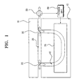
- a feature of the present invention is to provide a polarization mode dispersion compensation apparatus using a photonic crystal structure.
Landscapes
- Physics & Mathematics (AREA)
- Engineering & Computer Science (AREA)
- Optics & Photonics (AREA)
- Nonlinear Science (AREA)
- General Physics & Mathematics (AREA)
- Nanotechnology (AREA)
- Chemical & Material Sciences (AREA)
- Microelectronics & Electronic Packaging (AREA)
- Computer Networks & Wireless Communication (AREA)
- Signal Processing (AREA)
- Life Sciences & Earth Sciences (AREA)
- Biophysics (AREA)
- Crystallography & Structural Chemistry (AREA)
- Electromagnetism (AREA)
- Optical Integrated Circuits (AREA)
- Optical Modulation, Optical Deflection, Nonlinear Optics, Optical Demodulation, Optical Logic Elements (AREA)
Applications Claiming Priority (2)
| Application Number | Priority Date | Filing Date | Title |
|---|---|---|---|
| KR2002047167 | 2002-08-09 | ||
| KR10-2002-0047167A KR100430995B1 (ko) | 2002-08-09 | 2002-08-09 | 포토닉 크리스탈 구조를 이용한 편광모드분산 보상장치 |
Publications (3)
| Publication Number | Publication Date |
|---|---|
| EP1388962A2 true EP1388962A2 (de) | 2004-02-11 |
| EP1388962A3 EP1388962A3 (de) | 2005-07-13 |
| EP1388962B1 EP1388962B1 (de) | 2008-09-10 |
Family
ID=30439427
Family Applications (1)
| Application Number | Title | Priority Date | Filing Date |
|---|---|---|---|
| EP03018136A Expired - Lifetime EP1388962B1 (de) | 2002-08-09 | 2003-08-08 | Kompensationsvorrichtung der Polarisationsmodendispersion mittels einer Photonenkristallstruktur |
Country Status (5)
| Country | Link |
|---|---|
| US (1) | US7206513B2 (de) |
| EP (1) | EP1388962B1 (de) |
| JP (1) | JP3990660B2 (de) |
| KR (1) | KR100430995B1 (de) |
| DE (1) | DE60323434D1 (de) |
Families Citing this family (2)
| Publication number | Priority date | Publication date | Assignee | Title |
|---|---|---|---|---|
| KR100701147B1 (ko) | 2005-10-28 | 2007-03-28 | 한국전자통신연구원 | 광통신 시스템에 사용되는 분산 보상을 위한 장치 및 방법 |
| US8705898B2 (en) * | 2007-06-15 | 2014-04-22 | The Trustees Of Columbia University In The City Of New York | Systems, devices and methods for tuning a resonant wavelength of an optical resonator and dispersion properties of a photonic crystal waveguide |
Family Cites Families (14)
| Publication number | Priority date | Publication date | Assignee | Title |
|---|---|---|---|---|
| US5600738A (en) * | 1994-12-30 | 1997-02-04 | Lucent Technologies Inc. | Polarization dispersion compensation for optical devices |
| IT1282401B1 (it) * | 1996-05-03 | 1998-03-20 | Pirelli Cavi S P A Ora Pirelli | Dispositivo acusto -ottico in guida d'onda con compensazione di dispersione modale di polarizzazione |
| US5930414A (en) | 1997-09-16 | 1999-07-27 | Lucent Technologies Inc. | Method and apparatus for automatic compensation of first-order polarization mode dispersion (PMD) |
| WO1999028723A1 (en) | 1997-11-28 | 1999-06-10 | Fujitsu Limited | Polarization mode dispersion measuring method, and a dispersion compensation control device and a dispersion compensation control method |
| US6175671B1 (en) * | 1998-10-01 | 2001-01-16 | Nortel Networks Limited | Photonic crystal waveguide arrays |
| JP3493149B2 (ja) | 1998-10-23 | 2004-02-03 | 日本電信電話株式会社 | 偏光子とその製造方法及びこれを用いた導波型光デバイス |
| JP3348431B2 (ja) * | 1999-01-29 | 2002-11-20 | 日本電気株式会社 | 分散補償光回路 |
| JP3608983B2 (ja) | 1999-07-09 | 2005-01-12 | 日本電信電話株式会社 | 偏波分散補償回路 |
| US6493473B1 (en) * | 1999-08-03 | 2002-12-10 | Uniphase Telecommunciations Products, Inc. | Method and apparatus for providing transformation of the polarization of light |
| US6674949B2 (en) | 2000-08-15 | 2004-01-06 | Corning Incorporated | Active photonic crystal waveguide device and method |
| WO2002019001A2 (en) | 2000-09-01 | 2002-03-07 | University Of Southern California | Compensation and control of both first-order and higher-order polarization-mode dispersion |
| JP2002082239A (ja) * | 2000-09-11 | 2002-03-22 | Nec Corp | フォトニック結晶およびこれを用いた光パルス制御装置 |
| JP3467467B2 (ja) | 2000-10-20 | 2003-11-17 | 株式会社日立製作所 | 光制御素子 |
| JP2002196296A (ja) | 2000-12-25 | 2002-07-12 | Mitsubishi Electric Corp | 光変調器 |
-
2002
- 2002-08-09 KR KR10-2002-0047167A patent/KR100430995B1/ko not_active Expired - Fee Related
-
2003
- 2003-08-08 US US10/636,735 patent/US7206513B2/en not_active Expired - Fee Related
- 2003-08-08 DE DE60323434T patent/DE60323434D1/de not_active Expired - Lifetime
- 2003-08-08 EP EP03018136A patent/EP1388962B1/de not_active Expired - Lifetime
- 2003-08-11 JP JP2003291083A patent/JP3990660B2/ja not_active Expired - Fee Related
Also Published As
| Publication number | Publication date |
|---|---|
| US20040114937A1 (en) | 2004-06-17 |
| EP1388962A3 (de) | 2005-07-13 |
| KR20040014004A (ko) | 2004-02-14 |
| JP3990660B2 (ja) | 2007-10-17 |
| KR100430995B1 (ko) | 2004-05-20 |
| EP1388962B1 (de) | 2008-09-10 |
| JP2004078213A (ja) | 2004-03-11 |
| DE60323434D1 (de) | 2008-10-23 |
| US7206513B2 (en) | 2007-04-17 |
Similar Documents
| Publication | Publication Date | Title |
|---|---|---|
| US4673270A (en) | Channel add/drop filter-coupler | |
| EP0627640B1 (de) | Trennung von mehreren Lichtsignalen mit unterschiedlichen Frequenzen mittels ungleicher optischer Fasern | |
| US6445862B1 (en) | Dispersion compensating photonic crystal fiber | |
| US6259847B1 (en) | Optical communication system including broadband all-pass filter for dispersion compensation | |
| EP3973337A1 (de) | Integrierter optischer polarisator und verfahren zu seiner herstellung | |
| US20030169987A1 (en) | Tunable microfluidic optical fiber devices and systems | |
| EP0145124A2 (de) | Polarisator für Faseroptik | |
| US4668264A (en) | Method for making self-aligning optical fiber with accessible guiding region | |
| US5636300A (en) | MxO multiplex demultiplex component | |
| EP0135359A2 (de) | Schaltbarer Fiberoptischer Koppler | |
| US6400869B2 (en) | Tunable compensation for polarization-mode dispersion using a birefringent nonlinearly-chirped bragg grating in a dual-pass configuration | |
| US6826342B1 (en) | Temperature tuning of dispersion in photonic band gap fiber | |
| US6233375B1 (en) | Integrated optics component with polarization effect | |
| JP4504561B2 (ja) | 可変光ファイバ・ブラッグ・長周期グレーティング | |
| WO1987004261A1 (en) | Optical coupler | |
| US6928199B2 (en) | Tunable optical device for dynamic chromatic dispersion and polarization mode dispersion compensation | |
| EP1388962B1 (de) | Kompensationsvorrichtung der Polarisationsmodendispersion mittels einer Photonenkristallstruktur | |
| US4976512A (en) | Narrowband fiberoptic spectral filter formed from fibers having a refractive index with a W profile and a step profile | |
| EP0021712A1 (de) | Dielektrische Wellenleiter und Verfahren zur Ausbreitung polarisierter elektromagnetischer Wellen und ein Kommunikationsgerät und System das solche Wellenleiter und Verfahren verwendet | |
| US6711327B2 (en) | Device and method for compensating for chromatic dispersion | |
| US6515778B1 (en) | Polarization mode dispersion compensation | |
| EP0308244A2 (de) | Wellenlängen selektiver optischer Richtkoppler | |
| US7016584B2 (en) | Photonic bandgap optical fiber | |
| Andreev et al. | Wavelength division action of a distributed single-mode fiber-to-symmetrical planar waveguide coupler | |
| EP0202629A2 (de) | Optische Geräte und Systeme mit optischen Wellenleiterverbindungen |
Legal Events
| Date | Code | Title | Description |
|---|---|---|---|
| PUAI | Public reference made under article 153(3) epc to a published international application that has entered the european phase |
Free format text: ORIGINAL CODE: 0009012 |
|
| 17P | Request for examination filed |
Effective date: 20030808 |
|
| AK | Designated contracting states |
Kind code of ref document: A2 Designated state(s): AT BE BG CH CY CZ DE DK EE ES FI FR GB GR HU IE IT LI LU MC NL PT RO SE SI SK TR |
|
| AX | Request for extension of the european patent |
Extension state: AL LT LV MK |
|
| PUAL | Search report despatched |
Free format text: ORIGINAL CODE: 0009013 |
|
| AK | Designated contracting states |
Kind code of ref document: A3 Designated state(s): AT BE BG CH CY CZ DE DK EE ES FI FR GB GR HU IE IT LI LU MC NL PT RO SE SI SK TR |
|
| AX | Request for extension of the european patent |
Extension state: AL LT LV MK |
|
| RIC1 | Information provided on ipc code assigned before grant |
Ipc: 7G 02B 6/122 B Ipc: 7G 02F 1/01 B Ipc: 7H 04B 10/18 A |
|
| AKX | Designation fees paid |
Designated state(s): DE FR GB |
|
| 17Q | First examination report despatched |
Effective date: 20061130 |
|
| GRAP | Despatch of communication of intention to grant a patent |
Free format text: ORIGINAL CODE: EPIDOSNIGR1 |
|
| GRAS | Grant fee paid |
Free format text: ORIGINAL CODE: EPIDOSNIGR3 |
|
| GRAA | (expected) grant |
Free format text: ORIGINAL CODE: 0009210 |
|
| AK | Designated contracting states |
Kind code of ref document: B1 Designated state(s): DE FR GB |
|
| REG | Reference to a national code |
Ref country code: GB Ref legal event code: FG4D |
|
| REF | Corresponds to: |
Ref document number: 60323434 Country of ref document: DE Date of ref document: 20081023 Kind code of ref document: P |
|
| PLBE | No opposition filed within time limit |
Free format text: ORIGINAL CODE: 0009261 |
|
| STAA | Information on the status of an ep patent application or granted ep patent |
Free format text: STATUS: NO OPPOSITION FILED WITHIN TIME LIMIT |
|
| 26N | No opposition filed |
Effective date: 20090611 |
|
| PGFP | Annual fee paid to national office [announced via postgrant information from national office to epo] |
Ref country code: DE Payment date: 20130725 Year of fee payment: 11 |
|
| PGFP | Annual fee paid to national office [announced via postgrant information from national office to epo] |
Ref country code: GB Payment date: 20130729 Year of fee payment: 11 Ref country code: FR Payment date: 20130725 Year of fee payment: 11 |
|
| REG | Reference to a national code |
Ref country code: DE Ref legal event code: R119 Ref document number: 60323434 Country of ref document: DE |
|
| REG | Reference to a national code |
Ref country code: DE Ref legal event code: R079 Ref document number: 60323434 Country of ref document: DE Free format text: PREVIOUS MAIN CLASS: H04B0010180000 Ipc: H04B0010250700 |
|
| GBPC | Gb: european patent ceased through non-payment of renewal fee |
Effective date: 20140808 |
|
| REG | Reference to a national code |
Ref country code: FR Ref legal event code: ST Effective date: 20150430 |
|
| REG | Reference to a national code |
Ref country code: DE Ref legal event code: R119 Ref document number: 60323434 Country of ref document: DE Effective date: 20150303 Ref country code: DE Ref legal event code: R079 Ref document number: 60323434 Country of ref document: DE Free format text: PREVIOUS MAIN CLASS: H04B0010180000 Ipc: H04B0010250700 Effective date: 20150428 |
|
| PG25 | Lapsed in a contracting state [announced via postgrant information from national office to epo] |
Ref country code: GB Free format text: LAPSE BECAUSE OF NON-PAYMENT OF DUE FEES Effective date: 20140808 Ref country code: DE Free format text: LAPSE BECAUSE OF NON-PAYMENT OF DUE FEES Effective date: 20150303 |
|
| PG25 | Lapsed in a contracting state [announced via postgrant information from national office to epo] |
Ref country code: FR Free format text: LAPSE BECAUSE OF NON-PAYMENT OF DUE FEES Effective date: 20140901 |