EP1389820A2 - Disposition de circuit à faible inductance pour moduls à sémi-conducteur de puissance - Google Patents
Disposition de circuit à faible inductance pour moduls à sémi-conducteur de puissance Download PDFInfo
- Publication number
- EP1389820A2 EP1389820A2 EP03016373A EP03016373A EP1389820A2 EP 1389820 A2 EP1389820 A2 EP 1389820A2 EP 03016373 A EP03016373 A EP 03016373A EP 03016373 A EP03016373 A EP 03016373A EP 1389820 A2 EP1389820 A2 EP 1389820A2
- Authority
- EP
- European Patent Office
- Prior art keywords
- circuit arrangement
- connection
- substrate
- power semiconductor
- arrangement according
- Prior art date
- Legal status (The legal status is an assumption and is not a legal conclusion. Google has not performed a legal analysis and makes no representation as to the accuracy of the status listed.)
- Granted
Links
Images


Classifications
-
- H—ELECTRICITY
- H02—GENERATION; CONVERSION OR DISTRIBUTION OF ELECTRIC POWER
- H02M—APPARATUS FOR CONVERSION BETWEEN AC AND AC, BETWEEN AC AND DC, OR BETWEEN DC AND DC, AND FOR USE WITH MAINS OR SIMILAR POWER SUPPLY SYSTEMS; CONVERSION OF DC OR AC INPUT POWER INTO SURGE OUTPUT POWER; CONTROL OR REGULATION THEREOF
- H02M7/00—Conversion of AC power input into DC power output; Conversion of DC power input into AC power output
- H02M7/003—Constructional details, e.g. physical layout, assembly, wiring or busbar connections
-
- H—ELECTRICITY
- H10—SEMICONDUCTOR DEVICES; ELECTRIC SOLID-STATE DEVICES NOT OTHERWISE PROVIDED FOR
- H10W—GENERIC PACKAGES, INTERCONNECTIONS, CONNECTORS OR OTHER CONSTRUCTIONAL DETAILS OF DEVICES COVERED BY CLASS H10
- H10W44/00—Electrical arrangements for controlling or matching impedance
- H10W44/501—Inductive arrangements
-
- H—ELECTRICITY
- H10—SEMICONDUCTOR DEVICES; ELECTRIC SOLID-STATE DEVICES NOT OTHERWISE PROVIDED FOR
- H10W—GENERIC PACKAGES, INTERCONNECTIONS, CONNECTORS OR OTHER CONSTRUCTIONAL DETAILS OF DEVICES COVERED BY CLASS H10
- H10W90/00—Package configurations
-
- H—ELECTRICITY
- H10—SEMICONDUCTOR DEVICES; ELECTRIC SOLID-STATE DEVICES NOT OTHERWISE PROVIDED FOR
- H10W—GENERIC PACKAGES, INTERCONNECTIONS, CONNECTORS OR OTHER CONSTRUCTIONAL DETAILS OF DEVICES COVERED BY CLASS H10
- H10W72/00—Interconnections or connectors in packages
- H10W72/50—Bond wires
- H10W72/531—Shapes of wire connectors
- H10W72/533—Cross-sectional shape
- H10W72/534—Cross-sectional shape being rectangular
-
- H—ELECTRICITY
- H10—SEMICONDUCTOR DEVICES; ELECTRIC SOLID-STATE DEVICES NOT OTHERWISE PROVIDED FOR
- H10W—GENERIC PACKAGES, INTERCONNECTIONS, CONNECTORS OR OTHER CONSTRUCTIONAL DETAILS OF DEVICES COVERED BY CLASS H10
- H10W72/00—Interconnections or connectors in packages
- H10W72/50—Bond wires
- H10W72/531—Shapes of wire connectors
- H10W72/5363—Shapes of wire connectors the connected ends being wedge-shaped
-
- H—ELECTRICITY
- H10—SEMICONDUCTOR DEVICES; ELECTRIC SOLID-STATE DEVICES NOT OTHERWISE PROVIDED FOR
- H10W—GENERIC PACKAGES, INTERCONNECTIONS, CONNECTORS OR OTHER CONSTRUCTIONAL DETAILS OF DEVICES COVERED BY CLASS H10
- H10W72/00—Interconnections or connectors in packages
- H10W72/50—Bond wires
- H10W72/541—Dispositions of bond wires
- H10W72/5445—Dispositions of bond wires being orthogonal to a side surface of the chip, e.g. parallel arrangements
-
- H—ELECTRICITY
- H10—SEMICONDUCTOR DEVICES; ELECTRIC SOLID-STATE DEVICES NOT OTHERWISE PROVIDED FOR
- H10W—GENERIC PACKAGES, INTERCONNECTIONS, CONNECTORS OR OTHER CONSTRUCTIONAL DETAILS OF DEVICES COVERED BY CLASS H10
- H10W72/00—Interconnections or connectors in packages
- H10W72/50—Bond wires
- H10W72/541—Dispositions of bond wires
- H10W72/547—Dispositions of multiple bond wires
- H10W72/5473—Dispositions of multiple bond wires multiple bond wires connected to a common bond pad
-
- H—ELECTRICITY
- H10—SEMICONDUCTOR DEVICES; ELECTRIC SOLID-STATE DEVICES NOT OTHERWISE PROVIDED FOR
- H10W—GENERIC PACKAGES, INTERCONNECTIONS, CONNECTORS OR OTHER CONSTRUCTIONAL DETAILS OF DEVICES COVERED BY CLASS H10
- H10W72/00—Interconnections or connectors in packages
- H10W72/50—Bond wires
- H10W72/541—Dispositions of bond wires
- H10W72/547—Dispositions of multiple bond wires
- H10W72/5475—Dispositions of multiple bond wires multiple bond wires connected to common bond pads at both ends of the wires
-
- H—ELECTRICITY
- H10—SEMICONDUCTOR DEVICES; ELECTRIC SOLID-STATE DEVICES NOT OTHERWISE PROVIDED FOR
- H10W—GENERIC PACKAGES, INTERCONNECTIONS, CONNECTORS OR OTHER CONSTRUCTIONAL DETAILS OF DEVICES COVERED BY CLASS H10
- H10W72/00—Interconnections or connectors in packages
- H10W72/90—Bond pads, in general
- H10W72/921—Structures or relative sizes of bond pads
- H10W72/926—Multiple bond pads having different sizes
-
- H—ELECTRICITY
- H10—SEMICONDUCTOR DEVICES; ELECTRIC SOLID-STATE DEVICES NOT OTHERWISE PROVIDED FOR
- H10W—GENERIC PACKAGES, INTERCONNECTIONS, CONNECTORS OR OTHER CONSTRUCTIONAL DETAILS OF DEVICES COVERED BY CLASS H10
- H10W90/00—Package configurations
- H10W90/701—Package configurations characterised by the relative positions of pads or connectors relative to package parts
- H10W90/751—Package configurations characterised by the relative positions of pads or connectors relative to package parts of bond wires
- H10W90/753—Package configurations characterised by the relative positions of pads or connectors relative to package parts of bond wires between laterally-adjacent chips
-
- H—ELECTRICITY
- H10—SEMICONDUCTOR DEVICES; ELECTRIC SOLID-STATE DEVICES NOT OTHERWISE PROVIDED FOR
- H10W—GENERIC PACKAGES, INTERCONNECTIONS, CONNECTORS OR OTHER CONSTRUCTIONAL DETAILS OF DEVICES COVERED BY CLASS H10
- H10W90/00—Package configurations
- H10W90/701—Package configurations characterised by the relative positions of pads or connectors relative to package parts
- H10W90/751—Package configurations characterised by the relative positions of pads or connectors relative to package parts of bond wires
- H10W90/756—Package configurations characterised by the relative positions of pads or connectors relative to package parts of bond wires between a chip and a stacked lead frame, conducting package substrate or heat sink
Definitions
- the invention describes a compact, low-inductance circuit arrangement for modern power semiconductor modules in which the use is fast and low loss switching semiconductor switch is preferred.
- power semiconductor components are for This circuit arrangement therefore particularly MOSFETs or Insulated Gate Bipolar- Transistors (IGBT) with antiparallel connected freewheeling diodes suitable.
- IGBT Insulated Gate Bipolar- Transistors
- Such Circuitry and thus constructed as an example power converter must low inductively designed to the emergence of voltage spikes in particular to avoid during shutdowns. This means that stray inductances in the DC link, on the connecting conductors as well as on the substrate surface of the Circuit arrangement must be small. Litter inductances, which in their sum the Range of about 20 nH, with low-voltage MOSFET can already too Voltage peaks that can destroy the power semiconductor switches.
- the invention is suitable for the construction of rectifier arrangements, in which preferably power diodes and / or power thyristors are used.
- the prior art includes individual switches and power semiconductor modules with individual constructive measures to reduce parasitic inductances, as e.g. known are from EP 0 277 546, DE 39 37 045 or DE 100 37 533.
- the state of the art still includes compact power semiconductor modules like them are described by way of example in DE 197 19 703.
- Such power semiconductor modules consist of ceramic substrates with connecting lanes applied to them which semiconductor components are arranged. These semiconductor devices are by means of Soldering connected to the interconnect lines and have bond connections to others Semiconductor devices on.
- the connection elements located on the housing wall have partial surfaces, starting from which Drahtbondeducationen to individual Connecting tracks of the substrate are produced.
- the object of the present invention is a circuit arrangement to present low parasitic inductances of the entire arrangement, the a reduced ohmic resistance of the power supply and discharge to the Has semiconductor devices and a low total area requirement for the Semiconductor devices and the connection conductors, wherein the connection conductors for Semiconductor devices only slightly reduce usable area of the substrate.
- An advantage of the inventive design of the circuit arrangement is in addition to the low parasitic inductances and by o.g. Arrangement realizable compact Dimensions also the lower ohmic resistance of the leads to the Semiconductor devices, since the current flows substantially within the connection conductors and only a comparatively short distance within the lanes, which after have a higher ohmic resistance in the prior art.
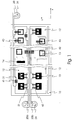
- Fig. 1 shows schematically partial aspects of an inventive Circuit arrangement in plan view to the various possible embodiments display.
- the circuit arrangement consists of a substrate (10), which after the State of the art as an insulating ceramic exemplified by alumina is. On this substrate are metallic according to a Therapeuticverbindehabilit Connection webs (12) applied. These connecting tracks form individual isolated areas on the ceramic substrate (10).
- Such combinations a ceramic substrate (10) and disposed thereon according to the circuit Tie tracks are exemplified as DCB (direct copper bonding) substrates and are widely used for power semiconductor modules.
- DCB direct copper bonding
- DCB substrate (10, 12) On the DCB substrate (10, 12) are a plurality of power semiconductor devices (13) cohesively applied by soldering.
- power semiconductor modules have as Power semiconductor devices IGBTs (insulated gate bipolar transistor) and with these proven antiparallel freewheeling diodes or MOS-FETs. Alternatively, too Thyristors are used.
- IGBTs insulated gate bipolar transistor
- MOS-FETs insulated gate bipolar transistor
- Thyristors are used.
- further components (14) such as For example, arranged current or temperature sensors.
- the connections of the Power semiconductor components (13) with further connecting tracks (12) is after the State of the art usually achieved by means of wire bonds (43).
- the circuit connection conductor (20, 30) For electrically connecting the power semiconductor components with external terminals has the circuit connection conductor (20, 30). These are each by one formed flat metal body, the external contact contact elements (24, 34) has, which are designed as screw connections.
- a not shown housing has Recesses for the connection conductors (20, 30), said by the said Recesses protrude outwards.
- the DC connection conductors (20a, 20b) are parasitic to achieve less Inductors closely adjacent in their entire course and only by one to the electrical Isolation of the two necessary layer separated from each other. Furthermore, it is advantageous to achieve the lowest possible parasitic inductances, if the DC connection conductor (20) in substantial sections closely adjacent to Substrate (10) and / or arranged to the connecting tracks. For this, however, must an electrical insulation between the connecting track and the connecting conductor be arranged unless an electrical connection between them is appropriate.
- the AC connection conductor (30) is arranged such that the shortest possible Wire bonds to its associated connecting tracks and / or Semiconductor devices are possible. This is advantageous, as a result of this a compact construction the power semiconductor module is possible.
- connection conductors (20, 30) can have recesses (see FIGS. 3 to 23) in which Do not place the connecting leads close to the substrate or the Connecting tracks are arranged to exemplify wire bonding connections (42) between other circuit parts, here two connection tracks (12) to allow.
- connection conductors (20, 30) For internal contacting, ie contacting to power semiconductor components (13) and / or with connecting tracks (12), the connection conductors (20, 30) have a plurality of surface elements (21, 31). These surface elements are considered a parallel to the Substrate arranged tab of the connecting conductor formed. This tab points to her side facing away from the substrate, a sufficiently large area on around bond feet, so the Contacting wire bonds (40, 41) to record.
- This Surface elements (21, 31) and the wire bond connections (40, 41) emanating from them are the connection conductors circuit-compatible with connecting tracks (12) and / or with Semiconductor devices (13) contacted.
- a direct contact by means of a Wire bond connection (40) of the surface element (21, 31) with a semiconductor device (13) proves to be particularly advantageous, because thereby the land consumption of Contacting is minimal.
- Fig. 2 shows schematically parts of the circuit arrangement according to the invention according to Fig. 1 in Cross-section.
- the DCB substrate is not only from a ceramic substrate (10) and arranged on its upper side circuit-compatible interconnects (12), but also from a rule full-surface metal lamination (11) on the underside of the ceramic substrate, applied by the same method, in the same thickness and of the same metal, like the connecting tracks (12).
- a rule full-surface metal lamination (11) on the underside of the ceramic substrate, applied by the same method, in the same thickness and of the same metal, like the connecting tracks (12).
- Power semiconductor components (13) soldered Arranged on the circuit Connecting webs (12) on the top of the substrate are in turn Power semiconductor components (13) soldered.
- the DC connection conductors (20) are with their narrow longitudinal side to the substrate directed arranged and have additional surface elements (21). These Surface elements are designed such that starting from them Wire bonds to power semiconductor devices (13) and / or to Connecting tracks are possible.
- the two DC connection conductors (20) are narrow arranged adjacent to each other and electrically isolated only by an insulating film (25) and spaced apart.
- the AC connection conductor (30) points in an analogous manner to the DC connection conductors (20) also surface elements (31) for Wire bonds (41), in the form shown for electrical connection to serve a connection track (12), but also for connection to semiconductor devices (13) are suitable.
- connection conductors are closely adjacent to the substrate and / or to the Connecting tracks arranged.
- the spacers serve simultaneously as insulation layer for electrical insulation e.g. compared to the Connecting tracks (12). These spacers are below the connection conductors arranged.
- Insulating layer serving spacers (22) also below these surface elements (21, 31).
- the foot elements (26) make contact with the substrate (10). you are Part of the connection conductor (20, 30) and below or next to the surface elements (21, 31) arranged.
- the foot elements (26) serve as well as the spacers (22) in the Production of the wire bond connection to avoid vibrations of the Connection element.
- FIG. 3 shows again, here in a three-dimensional sketch, a connecting conductor (20, 30) the circuit arrangement according to the invention.
- the connecting conductor (20b) consists, like the another connecting conductor also, preferably from a flat metal body Copper with a refined, exemplified silvered, surface. At this metal body are arranged, for example by means of stamping-bending technique produced surface elements (21, 31) and foot elements (26).
- the surface elements are used for electrical contacting of connecting tracks (12) and / or semiconductor devices (13) by means of wire bond connections (40, 41).
- the Foot elements serve to support the connection conductor on one not with one Connecting track (12) provided part of the substrate (10).
- a connecting conductor can have one or more recesses (23) Example wire bonds at right angles to the course of the connecting conductor to allow (see Fig. 1 - 42).
- one or more recesses may serve that surface elements (21) of an adjacently arranged connection conductor under the Recessed connecting conductor protrude through (see Fig. 4 and 5 - 23).
- a spacer (22) is arranged for electrical isolation and / or spacing to the substrate and / or to Connecting tracks with effect analogous to the foot element is below the connecting conductor.
- This spacer (22a) can reach below the Surface elements (21, 31) be extended.
- Fig. 4 shows a circuit arrangement according to the invention in half-bridge topology.
- the both DC connection conductors (20a, 20b) are narrow in their entire course arranged adjacent to each other.
- the minus DC connection conductor (20a) indicates two points (23) recesses (see also Fig. 3 - 23), through which Surface elements (21) of the plus DC connection conductor (20b) protrude. Consequently have the two arranged on one longitudinal side of the half-bridge DC connection conductor Contact elements for contacting the connection tracks (12) or the power semiconductor components (13).
- the half bridge itself consists of two Circuit breakers, each formed by 3 IGBTs (13a). Each Circuit breaker is associated with a power diode (13b) and anti-parallel to it connected.
- the IGBTs associated with the first semiconductor switch arranged collectors are connected to the plus DC power connection conductor (21 b) or its surface elements (21) connected by these surface elements Wire bonding connections (41) to the connection tracks (12) assigned to these IGBTs are arranged.
- the cathode of the anti-parallel diode (13b) is connected to the plus DC connection conductor (20b).
- the emitters of these IGBTs are partly connected to each other by wire bonds (44) and directly to the AC connection conductor (30) by means of wire bond connections (40).
- the anode of Power diode (13b) is also wired via wire bonds (44) with an emitter an IGBT and its wirebond connection (40) with the AC connection conductor (30) connected.
- the collectors of the IGBTs (13a) of the second circuit breaker of the half-bridge are with the AC connection conductor (30) via wire bond connections (41) to the Connection paths (12) on which the IGBTs are arranged, connected.
- Analog is the Cathode of the antiparallel switched power diode (13b) with the AC connection conductor (30) connected.
- the emitters of the IGBTs as well as the anode of the Power diodes are connected via wire bonds (40, 44) directly to the minus DC connection conductor (20a).
- Fig. 5 shows a circuit arrangement according to the invention in 3-phase Inverter topology. This is basically a series of three Half bridges (see Fig. 4), wherein for simplicity, each circuit breaker by only one IGBT (13a) is represented.
- the DC connections (20) are analogous to that shown in Fig. 4, also with recesses (23) of the minus DC connection conductor (20a), so that surface elements (21) of the plus DC connection conductor (20b) can protrude around the circuit-compatible To be able to realize connections.
- the required three AC connection conductors are at the opposite side of the DC terminals Circuit arrangement arranged and each in the same manner as described under Fig. 4 contacted.
Landscapes
- Engineering & Computer Science (AREA)
- Power Engineering (AREA)
- Power Conversion In General (AREA)
- Rectifiers (AREA)
- Inverter Devices (AREA)
Applications Claiming Priority (2)
| Application Number | Priority Date | Filing Date | Title |
|---|---|---|---|
| DE10237561A DE10237561C1 (de) | 2002-08-16 | 2002-08-16 | Induktivitätsarme Schaltungsanordnung bzw. Schaltungsaufbau für Leistungshalbleitermodule |
| DE10237561 | 2002-08-16 |
Publications (3)
| Publication Number | Publication Date |
|---|---|
| EP1389820A2 true EP1389820A2 (fr) | 2004-02-18 |
| EP1389820A3 EP1389820A3 (fr) | 2005-03-30 |
| EP1389820B1 EP1389820B1 (fr) | 2014-09-10 |
Family
ID=28051357
Family Applications (1)
| Application Number | Title | Priority Date | Filing Date |
|---|---|---|---|
| EP03016373.7A Expired - Lifetime EP1389820B1 (fr) | 2002-08-16 | 2003-07-19 | Disposition de circuit à faible inductance pour modules à sémi-conducteur de puissance |
Country Status (4)
| Country | Link |
|---|---|
| US (1) | US7227259B2 (fr) |
| EP (1) | EP1389820B1 (fr) |
| JP (1) | JP2004080993A (fr) |
| DE (1) | DE10237561C1 (fr) |
Families Citing this family (45)
| Publication number | Priority date | Publication date | Assignee | Title |
|---|---|---|---|---|
| DE10316356B4 (de) * | 2003-04-10 | 2012-07-26 | Semikron Elektronik Gmbh & Co. Kg | Modular aufgebautes Leistungshalbleitermodul |
| JP4081611B2 (ja) * | 2003-11-19 | 2008-04-30 | 株式会社豊田自動織機 | 半導体装置 |
| US7301755B2 (en) * | 2003-12-17 | 2007-11-27 | Siemens Vdo Automotive Corporation | Architecture for power modules such as power inverters |
| US7230333B2 (en) | 2005-04-21 | 2007-06-12 | International Rectifier Corporation | Semiconductor package |
| US8253179B2 (en) * | 2005-05-13 | 2012-08-28 | Semiconductor Energy Laboratory Co., Ltd. | Semiconductor device and manufacturing method of the same |
| DE102005039278A1 (de) * | 2005-08-19 | 2007-02-22 | Semikron Elektronik Gmbh & Co. Kg | Leistungshalbleitermodul mit Leitungselement |
| US8069208B2 (en) * | 2006-04-21 | 2011-11-29 | Microsoft Corporation | Peer-to-peer buddy request and response |
| CN101819965B (zh) * | 2006-06-09 | 2013-01-16 | 本田技研工业株式会社 | 半导体装置 |
| EP2116858B1 (fr) | 2007-02-14 | 2013-01-02 | Alps Electric Co., Ltd. | Puce de capteur, dispositif de détection et procédé de fabrication de dispositif de détection |
| US7773381B2 (en) | 2007-09-26 | 2010-08-10 | Rohm Co., Ltd. | Semiconductor device |
| DE102008008853B4 (de) * | 2008-02-13 | 2010-05-06 | Semikron Elektronik Gmbh & Co. Kg | Schaltungsanordnung mit Bondverbindung |
| US8138585B2 (en) * | 2008-05-28 | 2012-03-20 | Fairchild Semiconductor Corporation | Four mosfet full bridge module |
| US20100149771A1 (en) * | 2008-12-16 | 2010-06-17 | Cree, Inc. | Methods and Apparatus for Flexible Mounting of Light Emitting Devices |
| CN101453158B (zh) * | 2008-12-26 | 2011-09-21 | 南京银茂微电子制造有限公司 | 一种用于小型变频器的功率模块 |
| DE102009024385B4 (de) * | 2009-06-09 | 2011-03-17 | Semikron Elektronik Gmbh & Co. Kg | Verfahren zur Herstellung eines Leistungshalbleitermoduls und Leistungshalbleitermodul mit einer Verbindungseinrichtung |
| DE102009029515A1 (de) * | 2009-09-16 | 2011-03-24 | Robert Bosch Gmbh | Leistungshalbleitermodul und Leistungshalbleiterschaltungsanordnung |
| US8076696B2 (en) | 2009-10-30 | 2011-12-13 | General Electric Company | Power module assembly with reduced inductance |
| DE102010002627B4 (de) | 2010-03-05 | 2023-10-05 | Infineon Technologies Ag | Niederinduktive Leistungshalbleiterbaugruppen |
| JP5370440B2 (ja) | 2011-08-31 | 2013-12-18 | 株式会社デンソー | 電子装置の製造方法 |
| US8637964B2 (en) * | 2011-10-26 | 2014-01-28 | Infineon Technologies Ag | Low stray inductance power module |
| JP5763026B2 (ja) * | 2012-09-24 | 2015-08-12 | 株式会社東芝 | 半導体装置 |
| US9571086B1 (en) | 2012-12-05 | 2017-02-14 | Lockheed Martin Corporation | Bi-directional switch |
| JP6102297B2 (ja) * | 2013-02-06 | 2017-03-29 | 富士電機株式会社 | 半導体装置 |
| KR102034717B1 (ko) * | 2013-02-07 | 2019-10-21 | 삼성전자주식회사 | 파워모듈용 기판, 파워모듈용 터미널 및 이들을 포함하는 파워모듈 |
| GB2515318B (en) * | 2013-06-19 | 2016-05-18 | Protean Electric Ltd | Inverter for an electric motor or generator |
| JP5975177B2 (ja) * | 2013-07-16 | 2016-08-23 | 三菱電機株式会社 | 半導体装置 |
| WO2016002385A1 (fr) | 2014-07-03 | 2016-01-07 | 日産自動車株式会社 | Module de semi-conducteur de puissance en demi-pont et son procédé de fabrication |
| DE102014219998B4 (de) | 2014-10-02 | 2020-09-24 | Vitesco Technologies GmbH | Leistungsmodul, Leistungsmodulgruppe, Leistungsendstufe sowie Antriebssystem mit einer Leistungsendstufe |
| WO2016084241A1 (fr) * | 2014-11-28 | 2016-06-02 | 日産自動車株式会社 | Module à semi-conducteur de puissance en demi-pont et procédé pour sa fabrication |
| US10396057B2 (en) * | 2015-02-13 | 2019-08-27 | Nissan Arc, Ltd. | Half-bridge power semiconductor module and method for manufacturing same |
| US10134718B2 (en) | 2015-07-09 | 2018-11-20 | Mitsubishi Electric Corporation | Power semiconductor module |
| US9972569B2 (en) * | 2016-04-12 | 2018-05-15 | General Electric Company | Robust low inductance power module package |
| EP3246945B1 (fr) | 2016-05-19 | 2018-10-03 | ABB Schweiz AG | Module de puissance à faible inductance parasite |
| JP6694589B2 (ja) * | 2016-06-02 | 2020-05-20 | 株式会社ジェイテクト | パワーモジュール |
| DE102016214741B4 (de) | 2016-08-09 | 2022-05-12 | Fraunhofer-Gesellschaft zur Förderung der angewandten Forschung e.V. | Aufbau für mindestens einen mit elektronischen und/oder elektrischen Bauelementen bestückten Träger |
| EP3613077B1 (fr) | 2017-05-02 | 2020-10-07 | ABB Power Grids Switzerland AG | Module en demi-pont ayant un agencement coaxial des bornes dc |
| JP6785729B2 (ja) * | 2017-07-12 | 2020-11-18 | 三菱電機株式会社 | パワーモジュール |
| CN107342313A (zh) * | 2017-08-15 | 2017-11-10 | 杭州浙阳电气有限公司 | 门极杂散均衡衬底及其功率半导体模块 |
| DE102018109996B4 (de) * | 2018-04-25 | 2020-06-04 | Semikron Elektronik Gmbh & Co. Kg | Leistungselektronische Schalteinrichtung |
| JP7135949B2 (ja) * | 2019-03-14 | 2022-09-13 | 株式会社デンソー | 電力変換装置 |
| WO2023107255A1 (fr) | 2021-12-08 | 2023-06-15 | Canoo Technologies Inc. | Module d'alimentation électrique à double pont à faible inductance avec détection intégrée |
| EP4243070B1 (fr) * | 2022-03-11 | 2025-05-21 | Hitachi Energy Ltd | Module de puissance et procédé de fabrication d'un module de puissance |
| DE102022205514A1 (de) * | 2022-05-31 | 2023-11-30 | Vitesco Technologies GmbH | Halbbrückenmodul mit parallel geführten Versorgungs-Zuleitungen verbunden mit isolierten Anschlussflächen zwischen zwei Streifenabschnitten sowie mit einem der Streifenabschnitte einer Leiterbahnschicht |
| IT202200013243A1 (it) * | 2022-06-22 | 2023-12-22 | St Microelectronics Srl | Modulo di potenza per circuito a semiponte con architettura scalabile e layout perfezionato |
| US20250080111A1 (en) * | 2023-08-29 | 2025-03-06 | Visic Technologies Ltd. | Low on-resistance high power switch |
Citations (5)
| Publication number | Priority date | Publication date | Assignee | Title |
|---|---|---|---|---|
| EP0277546A1 (fr) | 1987-01-21 | 1988-08-10 | Siemens Aktiengesellschaft | Dispositif semi-conducteur comprenant au moins un corps semi-conducteur |
| DE3937045A1 (de) | 1989-11-07 | 1991-05-08 | Abb Ixys Semiconductor Gmbh | Leistungshalbleitermodul |
| DE19719703A1 (de) | 1997-05-09 | 1998-11-12 | Eupec Gmbh & Co Kg | Leistungshalbleitermodul mit Keramiksubstrat |
| EP1143603A2 (fr) | 2000-03-30 | 2001-10-10 | Hitachi, Ltd. | Dispositif à semiconducteur et dispositif de conversion de puissance électrique |
| DE10037533C1 (de) | 2000-08-01 | 2002-01-31 | Semikron Elektronik Gmbh | Induktivitätsarme Schaltungsanordnung |
Family Cites Families (15)
| Publication number | Priority date | Publication date | Assignee | Title |
|---|---|---|---|---|
| EP0064856B1 (fr) * | 1981-05-12 | 1986-12-30 | LUCAS INDUSTRIES public limited company | Un arrangement à pont multi-phase |
| US4816984A (en) * | 1987-02-06 | 1989-03-28 | Siemens Aktiengesellschaft | Bridge arm with transistors and recovery diodes |
| US5731970A (en) * | 1989-12-22 | 1998-03-24 | Hitachi, Ltd. | Power conversion device and semiconductor module suitable for use in the device |
| JP3053298B2 (ja) * | 1992-08-19 | 2000-06-19 | 株式会社東芝 | 半導体装置 |
| DE59304797D1 (de) * | 1992-08-26 | 1997-01-30 | Eupec Gmbh & Co Kg | Leistungshalbleiter-Modul |
| JP2838625B2 (ja) * | 1992-09-08 | 1998-12-16 | 株式会社日立製作所 | 半導体モジュール |
| US5422440A (en) * | 1993-06-08 | 1995-06-06 | Rem Technologies, Inc. | Low inductance bus bar arrangement for high power inverters |
| DE69535775D1 (de) * | 1994-10-07 | 2008-08-07 | Hitachi Ltd | Halbleiteranordnung mit einer Mehrzahl von Halbleiterelementen |
| JPH0969603A (ja) * | 1995-09-01 | 1997-03-11 | Mitsubishi Electric Corp | 電力用半導体装置、その外装ケースとその製造方法 |
| JP3013794B2 (ja) * | 1996-12-10 | 2000-02-28 | 富士電機株式会社 | 半導体装置 |
| JP3521757B2 (ja) * | 1998-09-08 | 2004-04-19 | 株式会社豊田自動織機 | 半導体モジュール電極構造 |
| US20020034088A1 (en) * | 2000-09-20 | 2002-03-21 | Scott Parkhill | Leadframe-based module DC bus design to reduce module inductance |
| JP4461639B2 (ja) * | 2001-05-29 | 2010-05-12 | 株式会社豊田自動織機 | 半導体装置 |
| US6906404B2 (en) * | 2003-05-16 | 2005-06-14 | Ballard Power Systems Corporation | Power module with voltage overshoot limiting |
| US6987670B2 (en) * | 2003-05-16 | 2006-01-17 | Ballard Power Systems Corporation | Dual power module power system architecture |
-
2002
- 2002-08-16 DE DE10237561A patent/DE10237561C1/de not_active Expired - Fee Related
-
2003
- 2003-07-19 EP EP03016373.7A patent/EP1389820B1/fr not_active Expired - Lifetime
- 2003-08-14 JP JP2003293380A patent/JP2004080993A/ja active Pending
- 2003-08-18 US US10/643,391 patent/US7227259B2/en not_active Expired - Fee Related
Patent Citations (5)
| Publication number | Priority date | Publication date | Assignee | Title |
|---|---|---|---|---|
| EP0277546A1 (fr) | 1987-01-21 | 1988-08-10 | Siemens Aktiengesellschaft | Dispositif semi-conducteur comprenant au moins un corps semi-conducteur |
| DE3937045A1 (de) | 1989-11-07 | 1991-05-08 | Abb Ixys Semiconductor Gmbh | Leistungshalbleitermodul |
| DE19719703A1 (de) | 1997-05-09 | 1998-11-12 | Eupec Gmbh & Co Kg | Leistungshalbleitermodul mit Keramiksubstrat |
| EP1143603A2 (fr) | 2000-03-30 | 2001-10-10 | Hitachi, Ltd. | Dispositif à semiconducteur et dispositif de conversion de puissance électrique |
| DE10037533C1 (de) | 2000-08-01 | 2002-01-31 | Semikron Elektronik Gmbh | Induktivitätsarme Schaltungsanordnung |
Also Published As
| Publication number | Publication date |
|---|---|
| US7227259B2 (en) | 2007-06-05 |
| US20050024805A1 (en) | 2005-02-03 |
| JP2004080993A (ja) | 2004-03-11 |
| EP1389820A3 (fr) | 2005-03-30 |
| DE10237561C1 (de) | 2003-10-16 |
| EP1389820B1 (fr) | 2014-09-10 |
Similar Documents
| Publication | Publication Date | Title |
|---|---|---|
| DE10237561C1 (de) | Induktivitätsarme Schaltungsanordnung bzw. Schaltungsaufbau für Leistungshalbleitermodule | |
| DE102009002993B4 (de) | Leistungshalbleitermodul mit beabstandeten Schaltungsträgern | |
| DE102019112935B4 (de) | Halbleitermodul | |
| DE60127027T2 (de) | Halbleiterelement mit Leistungsverdrahtungsstruktur | |
| DE10037533C1 (de) | Induktivitätsarme Schaltungsanordnung | |
| EP1062698A1 (fr) | Module semi-conducteur electronique | |
| DE112015000156T5 (de) | Halbleitervorrichtung | |
| EP0776042A2 (fr) | Module semi-conducteur à haute puissance avec une pluralité de sous-modules | |
| EP0750345B1 (fr) | Module semi-conducteur de puissance | |
| DE19826731C2 (de) | Halbbrückenbaugruppe | |
| EP2532084A2 (fr) | Composant électronique pour commuter une puissance électrique | |
| DE102005036116B4 (de) | Leistungshalbleitermodul | |
| DE102020214045A1 (de) | Halbbrücke für einen elektrischen Antrieb eines Elektrofahrzeugs oder eines Hybridfahrzeugs, Leistungsmodul für einen Inverter und Inverter | |
| DE102004019443B3 (de) | Leistungsmodul | |
| DE102020106406B4 (de) | Leistungshalbleitermodul | |
| DE102004027185B4 (de) | Niederinduktives Halbleiterbauelement mit Halbbrückenkonfiguration | |
| DE60306040T2 (de) | Halbleitermodul und Leistungswandlervorrichtung | |
| DE102023208490B4 (de) | Leistungselektronikmodul und Montageverfahren | |
| DE102004046806A1 (de) | Leistungshalbleitermodul | |
| EP0710983B1 (fr) | Module à pont | |
| DE102019218953A1 (de) | Elektronische Schaltungseinheit | |
| DE102015115312B4 (de) | Halbleitermodul und Verfahren zum Betrieb eines Halbleitermoduls | |
| WO2000038306A1 (fr) | Inverseur de matrice | |
| EP3949103A1 (fr) | Unité de circuit électronique | |
| EP1755163B1 (fr) | Module semiconducteur de puissance avec segment de ligne |
Legal Events
| Date | Code | Title | Description |
|---|---|---|---|
| PUAI | Public reference made under article 153(3) epc to a published international application that has entered the european phase |
Free format text: ORIGINAL CODE: 0009012 |
|
| AK | Designated contracting states |
Kind code of ref document: A2 Designated state(s): AT BE BG CH CY CZ DE DK EE ES FI FR GB GR HU IE IT LI LU MC NL PT RO SE SI SK TR |
|
| AX | Request for extension of the european patent |
Extension state: AL LT LV MK |
|
| 17P | Request for examination filed |
Effective date: 20041130 |
|
| PUAL | Search report despatched |
Free format text: ORIGINAL CODE: 0009013 |
|
| AK | Designated contracting states |
Kind code of ref document: A3 Designated state(s): AT BE BG CH CY CZ DE DK EE ES FI FR GB GR HU IE IT LI LU MC NL PT RO SE SI SK TR |
|
| AX | Request for extension of the european patent |
Extension state: AL LT LV MK |
|
| RAP1 | Party data changed (applicant data changed or rights of an application transferred) |
Owner name: SEMIKRON ELEKTRONIK GMBH & CO. KG |
|
| AKX | Designation fees paid |
Designated state(s): AT BE BG CH CY CZ DE DK EE ES FI FR GB GR HU IE IT LI LU MC NL PT RO SE SI SK TR |
|
| REG | Reference to a national code |
Ref country code: DE Ref legal event code: R079 Ref document number: 50315126 Country of ref document: DE Free format text: PREVIOUS MAIN CLASS: H02J0007000000 Ipc: H02M0007720000 |
|
| RIC1 | Information provided on ipc code assigned before grant |
Ipc: H01L 27/088 20060101ALI20140331BHEP Ipc: H02M 7/72 20060101AFI20140331BHEP Ipc: H01L 25/04 20140101ALI20140331BHEP |
|
| GRAP | Despatch of communication of intention to grant a patent |
Free format text: ORIGINAL CODE: EPIDOSNIGR1 |
|
| INTG | Intention to grant announced |
Effective date: 20140603 |
|
| GRAS | Grant fee paid |
Free format text: ORIGINAL CODE: EPIDOSNIGR3 |
|
| GRAA | (expected) grant |
Free format text: ORIGINAL CODE: 0009210 |
|
| AK | Designated contracting states |
Kind code of ref document: B1 Designated state(s): AT BE BG CH CY CZ DE DK EE ES FI FR GB GR HU IE IT LI LU MC NL PT RO SE SI SK TR |
|
| REG | Reference to a national code |
Ref country code: GB Ref legal event code: FG4D Free format text: NOT ENGLISH |
|
| REG | Reference to a national code |
Ref country code: CH Ref legal event code: EP |
|
| REG | Reference to a national code |
Ref country code: IE Ref legal event code: FG4D Free format text: LANGUAGE OF EP DOCUMENT: GERMAN |
|
| REG | Reference to a national code |
Ref country code: AT Ref legal event code: REF Ref document number: 687133 Country of ref document: AT Kind code of ref document: T Effective date: 20141015 |
|
| REG | Reference to a national code |
Ref country code: DE Ref legal event code: R096 Ref document number: 50315126 Country of ref document: DE Effective date: 20141016 |
|
| PG25 | Lapsed in a contracting state [announced via postgrant information from national office to epo] |
Ref country code: ES Free format text: LAPSE BECAUSE OF FAILURE TO SUBMIT A TRANSLATION OF THE DESCRIPTION OR TO PAY THE FEE WITHIN THE PRESCRIBED TIME-LIMIT Effective date: 20140910 Ref country code: FI Free format text: LAPSE BECAUSE OF FAILURE TO SUBMIT A TRANSLATION OF THE DESCRIPTION OR TO PAY THE FEE WITHIN THE PRESCRIBED TIME-LIMIT Effective date: 20140910 Ref country code: GR Free format text: LAPSE BECAUSE OF FAILURE TO SUBMIT A TRANSLATION OF THE DESCRIPTION OR TO PAY THE FEE WITHIN THE PRESCRIBED TIME-LIMIT Effective date: 20141211 Ref country code: SE Free format text: LAPSE BECAUSE OF FAILURE TO SUBMIT A TRANSLATION OF THE DESCRIPTION OR TO PAY THE FEE WITHIN THE PRESCRIBED TIME-LIMIT Effective date: 20140910 |
|
| REG | Reference to a national code |
Ref country code: NL Ref legal event code: VDEP Effective date: 20140910 |
|
| PG25 | Lapsed in a contracting state [announced via postgrant information from national office to epo] |
Ref country code: CY Free format text: LAPSE BECAUSE OF FAILURE TO SUBMIT A TRANSLATION OF THE DESCRIPTION OR TO PAY THE FEE WITHIN THE PRESCRIBED TIME-LIMIT Effective date: 20140910 |
|
| PG25 | Lapsed in a contracting state [announced via postgrant information from national office to epo] |
Ref country code: NL Free format text: LAPSE BECAUSE OF FAILURE TO SUBMIT A TRANSLATION OF THE DESCRIPTION OR TO PAY THE FEE WITHIN THE PRESCRIBED TIME-LIMIT Effective date: 20140910 |
|
| PG25 | Lapsed in a contracting state [announced via postgrant information from national office to epo] |
Ref country code: PT Free format text: LAPSE BECAUSE OF FAILURE TO SUBMIT A TRANSLATION OF THE DESCRIPTION OR TO PAY THE FEE WITHIN THE PRESCRIBED TIME-LIMIT Effective date: 20150112 Ref country code: CZ Free format text: LAPSE BECAUSE OF FAILURE TO SUBMIT A TRANSLATION OF THE DESCRIPTION OR TO PAY THE FEE WITHIN THE PRESCRIBED TIME-LIMIT Effective date: 20140910 Ref country code: RO Free format text: LAPSE BECAUSE OF FAILURE TO SUBMIT A TRANSLATION OF THE DESCRIPTION OR TO PAY THE FEE WITHIN THE PRESCRIBED TIME-LIMIT Effective date: 20140910 Ref country code: EE Free format text: LAPSE BECAUSE OF FAILURE TO SUBMIT A TRANSLATION OF THE DESCRIPTION OR TO PAY THE FEE WITHIN THE PRESCRIBED TIME-LIMIT Effective date: 20140910 Ref country code: SK Free format text: LAPSE BECAUSE OF FAILURE TO SUBMIT A TRANSLATION OF THE DESCRIPTION OR TO PAY THE FEE WITHIN THE PRESCRIBED TIME-LIMIT Effective date: 20140910 |
|
| REG | Reference to a national code |
Ref country code: DE Ref legal event code: R097 Ref document number: 50315126 Country of ref document: DE |
|
| PLBE | No opposition filed within time limit |
Free format text: ORIGINAL CODE: 0009261 |
|
| STAA | Information on the status of an ep patent application or granted ep patent |
Free format text: STATUS: NO OPPOSITION FILED WITHIN TIME LIMIT |
|
| PG25 | Lapsed in a contracting state [announced via postgrant information from national office to epo] |
Ref country code: DK Free format text: LAPSE BECAUSE OF FAILURE TO SUBMIT A TRANSLATION OF THE DESCRIPTION OR TO PAY THE FEE WITHIN THE PRESCRIBED TIME-LIMIT Effective date: 20140910 |
|
| 26N | No opposition filed |
Effective date: 20150611 |
|
| PG25 | Lapsed in a contracting state [announced via postgrant information from national office to epo] |
Ref country code: IT Free format text: LAPSE BECAUSE OF FAILURE TO SUBMIT A TRANSLATION OF THE DESCRIPTION OR TO PAY THE FEE WITHIN THE PRESCRIBED TIME-LIMIT Effective date: 20140910 |
|
| PG25 | Lapsed in a contracting state [announced via postgrant information from national office to epo] |
Ref country code: SI Free format text: LAPSE BECAUSE OF FAILURE TO SUBMIT A TRANSLATION OF THE DESCRIPTION OR TO PAY THE FEE WITHIN THE PRESCRIBED TIME-LIMIT Effective date: 20140910 |
|
| PG25 | Lapsed in a contracting state [announced via postgrant information from national office to epo] |
Ref country code: MC Free format text: LAPSE BECAUSE OF FAILURE TO SUBMIT A TRANSLATION OF THE DESCRIPTION OR TO PAY THE FEE WITHIN THE PRESCRIBED TIME-LIMIT Effective date: 20140910 |
|
| REG | Reference to a national code |
Ref country code: CH Ref legal event code: PL |
|
| PG25 | Lapsed in a contracting state [announced via postgrant information from national office to epo] |
Ref country code: LU Free format text: LAPSE BECAUSE OF FAILURE TO SUBMIT A TRANSLATION OF THE DESCRIPTION OR TO PAY THE FEE WITHIN THE PRESCRIBED TIME-LIMIT Effective date: 20150719 |
|
| REG | Reference to a national code |
Ref country code: IE Ref legal event code: MM4A |
|
| PG25 | Lapsed in a contracting state [announced via postgrant information from national office to epo] |
Ref country code: LI Free format text: LAPSE BECAUSE OF NON-PAYMENT OF DUE FEES Effective date: 20150731 Ref country code: CH Free format text: LAPSE BECAUSE OF NON-PAYMENT OF DUE FEES Effective date: 20150731 |
|
| REG | Reference to a national code |
Ref country code: FR Ref legal event code: PLFP Year of fee payment: 14 |
|
| PG25 | Lapsed in a contracting state [announced via postgrant information from national office to epo] |
Ref country code: IE Free format text: LAPSE BECAUSE OF NON-PAYMENT OF DUE FEES Effective date: 20150719 |
|
| REG | Reference to a national code |
Ref country code: AT Ref legal event code: MM01 Ref document number: 687133 Country of ref document: AT Kind code of ref document: T Effective date: 20150719 |
|
| PG25 | Lapsed in a contracting state [announced via postgrant information from national office to epo] |
Ref country code: AT Free format text: LAPSE BECAUSE OF NON-PAYMENT OF DUE FEES Effective date: 20150719 |
|
| PG25 | Lapsed in a contracting state [announced via postgrant information from national office to epo] |
Ref country code: BG Free format text: LAPSE BECAUSE OF FAILURE TO SUBMIT A TRANSLATION OF THE DESCRIPTION OR TO PAY THE FEE WITHIN THE PRESCRIBED TIME-LIMIT Effective date: 20140910 Ref country code: HU Free format text: LAPSE BECAUSE OF FAILURE TO SUBMIT A TRANSLATION OF THE DESCRIPTION OR TO PAY THE FEE WITHIN THE PRESCRIBED TIME-LIMIT; INVALID AB INITIO Effective date: 20030719 |
|
| REG | Reference to a national code |
Ref country code: FR Ref legal event code: PLFP Year of fee payment: 15 |
|
| PG25 | Lapsed in a contracting state [announced via postgrant information from national office to epo] |
Ref country code: BE Free format text: LAPSE BECAUSE OF NON-PAYMENT OF DUE FEES Effective date: 20150731 |
|
| PG25 | Lapsed in a contracting state [announced via postgrant information from national office to epo] |
Ref country code: TR Free format text: LAPSE BECAUSE OF FAILURE TO SUBMIT A TRANSLATION OF THE DESCRIPTION OR TO PAY THE FEE WITHIN THE PRESCRIBED TIME-LIMIT Effective date: 20140910 |
|
| REG | Reference to a national code |
Ref country code: FR Ref legal event code: PLFP Year of fee payment: 16 |
|
| PGFP | Annual fee paid to national office [announced via postgrant information from national office to epo] |
Ref country code: FR Payment date: 20190724 Year of fee payment: 17 Ref country code: DE Payment date: 20190731 Year of fee payment: 17 |
|
| PGFP | Annual fee paid to national office [announced via postgrant information from national office to epo] |
Ref country code: GB Payment date: 20190725 Year of fee payment: 17 |
|
| REG | Reference to a national code |
Ref country code: DE Ref legal event code: R119 Ref document number: 50315126 Country of ref document: DE |
|
| GBPC | Gb: european patent ceased through non-payment of renewal fee |
Effective date: 20200719 |
|
| PG25 | Lapsed in a contracting state [announced via postgrant information from national office to epo] |
Ref country code: GB Free format text: LAPSE BECAUSE OF NON-PAYMENT OF DUE FEES Effective date: 20200719 Ref country code: FR Free format text: LAPSE BECAUSE OF NON-PAYMENT OF DUE FEES Effective date: 20200731 |
|
| PG25 | Lapsed in a contracting state [announced via postgrant information from national office to epo] |
Ref country code: DE Free format text: LAPSE BECAUSE OF NON-PAYMENT OF DUE FEES Effective date: 20210202 |