EP1391982A2 - Convertisseur courant continu-courant continu - Google Patents
Convertisseur courant continu-courant continu Download PDFInfo
- Publication number
- EP1391982A2 EP1391982A2 EP03019075A EP03019075A EP1391982A2 EP 1391982 A2 EP1391982 A2 EP 1391982A2 EP 03019075 A EP03019075 A EP 03019075A EP 03019075 A EP03019075 A EP 03019075A EP 1391982 A2 EP1391982 A2 EP 1391982A2
- Authority
- EP
- European Patent Office
- Prior art keywords
- circuit parts
- conversion circuit
- power source
- converter
- groups
- Prior art date
- Legal status (The legal status is an assumption and is not a legal conclusion. Google has not performed a legal analysis and makes no representation as to the accuracy of the status listed.)
- Withdrawn
Links
Images



Classifications
-
- H—ELECTRICITY
- H02—GENERATION; CONVERSION OR DISTRIBUTION OF ELECTRIC POWER
- H02M—APPARATUS FOR CONVERSION BETWEEN AC AND AC, BETWEEN AC AND DC, OR BETWEEN DC AND DC, AND FOR USE WITH MAINS OR SIMILAR POWER SUPPLY SYSTEMS; CONVERSION OF DC OR AC INPUT POWER INTO SURGE OUTPUT POWER; CONTROL OR REGULATION THEREOF
- H02M3/00—Conversion of DC power input into DC power output
- H02M3/22—Conversion of DC power input into DC power output with intermediate conversion into AC
- H02M3/24—Conversion of DC power input into DC power output with intermediate conversion into AC by static converters
- H02M3/28—Conversion of DC power input into DC power output with intermediate conversion into AC by static converters using discharge tubes with control electrode or semiconductor devices with control electrode to produce the intermediate AC
- H02M3/325—Conversion of DC power input into DC power output with intermediate conversion into AC by static converters using discharge tubes with control electrode or semiconductor devices with control electrode to produce the intermediate AC using devices of a triode or a transistor type requiring continuous application of a control signal
- H02M3/335—Conversion of DC power input into DC power output with intermediate conversion into AC by static converters using discharge tubes with control electrode or semiconductor devices with control electrode to produce the intermediate AC using devices of a triode or a transistor type requiring continuous application of a control signal using semiconductor devices only
- H02M3/337—Conversion of DC power input into DC power output with intermediate conversion into AC by static converters using discharge tubes with control electrode or semiconductor devices with control electrode to produce the intermediate AC using devices of a triode or a transistor type requiring continuous application of a control signal using semiconductor devices only in push-pull configuration
- H02M3/3376—Conversion of DC power input into DC power output with intermediate conversion into AC by static converters using discharge tubes with control electrode or semiconductor devices with control electrode to produce the intermediate AC using devices of a triode or a transistor type requiring continuous application of a control signal using semiconductor devices only in push-pull configuration with automatic control of output voltage or current
-
- H—ELECTRICITY
- H02—GENERATION; CONVERSION OR DISTRIBUTION OF ELECTRIC POWER
- H02M—APPARATUS FOR CONVERSION BETWEEN AC AND AC, BETWEEN AC AND DC, OR BETWEEN DC AND DC, AND FOR USE WITH MAINS OR SIMILAR POWER SUPPLY SYSTEMS; CONVERSION OF DC OR AC INPUT POWER INTO SURGE OUTPUT POWER; CONTROL OR REGULATION THEREOF
- H02M1/00—Details of apparatus for conversion
- H02M1/0067—Converter structures employing plural converter units, other than for parallel operation of the units on a single load
- H02M1/0077—Plural converter units whose outputs are connected in series
Definitions
- the present invention relates to a DC-DC converter, and particularly to a DC-DC converter which is used in a DC power source circuit and converts a power source voltage of a DC power source into a different DC voltage.
- a DC-DC converter used in a DC power source circuit is shown in Fig. 7.
- the DC-DC converter shown in Fig. 7 comprises a pair of conversion circuit parts 1, 2, two transformers Tr 1 , Tr 2 , a pair of rectification circuit parts 3, 4, and an LC smoothing circuit part 5.
- the pair of conversion circuit parts 1, 2 have two pairs of switching elements Q 1 , Q 4 , Q 2 , Q 3 and Q 5 , Q 8 , Q 6 , Q 7 which are connected by a full bridge configuration.
- the two transformers Tr 1 , Tr 2 are connected to the output sides of the conversion circuit parts 1, 2.
- the pair of rectification circuit parts 3, 4 are connected to secondary side outputs of the transformers Tr 1 , Tr 2 and are made of two pairs of diodes D 1 , D 4 , D 2 , D 3 and D 5 , D 8 , D 6 , D 7 .
- the LC smoothing circuit part 5 is connected in common with the output sides of the rectification circuit parts 3, 4.
- a pair of the conversion circuit parts 1, 2 are connected in parallel with a DC power source E.
- series capacitors C 1 , C 2 are inserted and connected between the output sides of each of the conversion circuit parts 1, 2 and the primary sides of the transformers Tr 1 , Tr 2 .
- the switching elements Q 1 , Q 4 , Q 2 , Q 3 and Q 5 , Q 8 , Q 6 , Q 7 of the conversion circuit parts 1, 2 are alternately turned on or off to obtain an AC waveform output.
- This AC waveform output of the conversion circuit parts 1, 2 is transformed by the transformers Tr 1 , Tr 2 and the secondary side outputs of the transformers Tr 1 , Tr 2 are rectified by the rectification circuit parts 3, 4 and also are smoothed by the LC smoothing circuit part 5. Therefore, a desired DC voltage V OUT is generated (for example, see JP-A-2002-223565).
- means for increasing a conversion capacity of the DC-DC converter described above means using a semiconductor device with large voltage and current or a large-size transformer in components forming the DC-DC converter can be implemented.
- the means for increasing a single device capacity of the DC-DC converter is undesirable because there are the problems described above. Therefore, as another means for increasing a conversion capacity of the DC-DC converter, it is considered that plural unitary units are connected in parallel with a DC power source E using a circuit configuration of the DC-DC converter shown in Fig. 7 as a unitary unit.
- a DC-DC converter having two unitary units A 1 , A 2 which are connected in parallel with a DC power source E is shown in Fig. 8.
- the unitary unit A 1 of the DC-DC converter shown in Fig. 8 provides a following configuration. That is, a pair of conversion circuit parts 11, 12 for converting a power source voltage of the DC power source E into an AC by switching elements Q 11 to Q 14 and Q 15 to Q 18 of a full bridge configuration are connected in parallel with the DC power source E. Rectification circuit parts 13, 14 made of diodes D 11 to D 14 and D 15 to D 18 are provided to the output sides of each of the conversion circuit parts 11, 12 through transformers Tr 11 , Tr 12 . Series capacitors C 11 , C 12 are inserted and connected between each of the conversion circuit parts 11, 12 and the transformers Tr 11 , Tr 12 .
- the unitary unit A 2 has the same circuit configuration as that of the unitary unit A 1 . That is, it comprises conversion circuit parts 21, 22 of parallel connection made of switching elements Q 21 to Q 24 and Q 25 to Q 28 of a full bridge configuration, and rectification circuit parts 23, 24 made of diodes D 21 to D 24 and D 25 to D 28 connected to the output sides of each of the conversion circuit parts 21, 22 through series capacitors C 21 , C 22 and transformers Tr 21 , Tr 22 .
- an LC smoothing circuit part 15 is provided to the output sides of the rectification circuit parts 13, 14, 23, 24.
- an object of the invention is to provide a DC-DC converter which can prevent an output current of a DC-DC converter from becoming an unbalance state even when there is a slight difference in output voltages of each conversion circuit part in the case of increasing a conversion capacity of the DC-DC converter.
- a DC-DC converter comprising:
- a conversion capacity of the DC-DC converter can be increased.
- the DC-DC converter has a configuration in which a pair of the conversion circuit parts in n groups of the unitary units are connected in parallel with the DC power source, but the invention is not limited to this.
- a configuration in which a pair of the conversion circuit parts are connected in series with the DC power source can also be used.
- n groups of the unitary units having a pair of the conversion circuit parts connected in series with the DC power source a configuration connected in either parallel or series with the DC power source can be used.
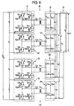
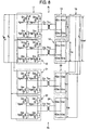
- Fig. 1 is a circuit diagram of a DC-DC converter in an embodiment of the invention.
- the DC-DC converter of this embodiment provides a circuit configuration in which n groups, for example, two groups of unitary units A 1 , A 2 are connected in parallel with a DC power source E. Incidentally, three or more groups of unitary units can be provided.
- One unitary unit A 1 provides a following configuration. That is, a pair of conversion circuit parts 11, 12 converts a power source voltage of the DC power source E into an AC by two pairs of switching elements Q 11 , Q 14 , Q 12 , Q 13 and Q 15 , Q 18 , Q 16 , Q 17 (for example, MOS-FET, bipolar transistor or IGBT) of a full bridge configuration.
- the pair of conversion circuit parts 11, 12 are connected in parallel with the DC power source E.
- Rectification circuit parts 13, 14 made of two pairs of diodes D 11 , D 14 , D 12 , D 13 and D 15 , D 18 , D 16 , D 17 are provided to the output sides of each of the conversion circuit parts 11, 12 through transformers Tr 11 , Tr 12 .
- Series capacitors C 11 , C 12 are inserted and connected between each of the conversion circuit parts 11, 12 and the transformers Tr 11 , Tr 12 .
- the other unitary unit A 2 has the same circuit configuration as that of the unitary unit A 1 . That is, it comprises two conversion circuit parts 21, 22, two transformers Tr 21 , Tr 22 , series capacitors C 21 , C 22 and rectification circuit parts 23, 24.
- the two conversion circuit parts 21, 22 have two pairs of switching elements Q 21 , Q 24 , Q 22 , Q 23 and Q 25 , Q 28 , Q 26 , Q 27 (for example, MOS-FET, bipolar transistor or IGBT) which are connected by a full bridge configuration and are connected in parallel with the DC power source E.
- the two transformers Tr 21 , Tr 22 are connected to each of the output sides of their conversion circuit parts 21, 22.
- the series capacitors C 21 , C 22 are inserted and connected between the output sides of each of the conversion circuit parts 21, 22 and the primary sides of the transformers Tr 21 , Tr 22 .
- the rectification circuit parts 23, 24 are connected to secondary side outputs of the transformers Tr 21 , Tr 22 and made of two pairs of diodes D 21 , D 24 , D 22 , D 23 and D 25 , D 28 , D 26 , D 27 .
- An operation of one unitary unit A 1 in this DC-DC converter is as follows. Incidentally, an operation of the other unitary unit A 2 is similar, so that operation description of the other unitary unit A 2 will be omitted.
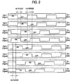
- Fig. 2 shows a timing chart of gate signals Vgs 11 to Vgs 14 , Vgs 15 to Vgs 18 for turning on or off each of the switching elements Q 11 to Q 14 , Q 15 to Q 18 of the DC-DC converter.
- the switching elements Q 11 , Q 14 , Q 12 , Q 13 and Q 15 , Q 18 , Q 16 , Q 17 of the conversion circuit parts 11, 12 are alternately turned on or off to obtain an AC waveform output.
- This AC waveform. output of the conversion circuit parts 11, 12 is transformed by the transformers Tr 11 , Tr 12 .
- the the secondary side of outputs the transformers Tr 11 , Tr 12 are rectified by the rectification circuit parts 13, 14 made of the diodes D 11 to D 14 , D 15 to D 18 and thereby, a desired DC voltage V OUT is generated.
- a switching phase of the other switching element Q 14 (the switching element Q 13 is inversion of the switching element Q 14 ) is delayed by a 1/3n period (1/6 period in the case of this embodiment) with respect to one switching element Q 11 (the switching element Q 12 is inversion of the switching element Q 11 ) of the switching elements Q 11 , Q 14 paired in one conversion circuit part 11.
- a switching phase of the switching element Q 15 (the switching element Q 16 is inversion of the switching element Q 15 ) of the other conversion circuit part 12 is delayed by a 1/2n period (1/4 period in the case of this embodiment) with respect to the switching element Q 11 .
- a switching phase of the other switching element Q 18 (the switching element Q 17 is inversion of the switching element Q 18 ) is delayed by a 1/6 period with respect to one switching element Q 15 (the switching element Q 16 is inversion of the switching element Q 15 ) of the switching elements Q 15 , Q 18 paired in the other conversion circuit part 12.
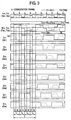
- Fig. 3 is a waveform chart of respective output voltages V 11 , V 12 of the rectification circuit parts 13, 14, primary side voltages of the transformers Tr 11 , Tr 12 , voltages Vds between drain and source of each of the switching elements Q 11 to Q 14 , Q 15 to Q 18 , and drain currents Id.
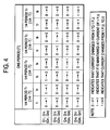
- the switching elements Q 11 to Q 14 , Q 15 to Q 18 of the conversion circuit parts 11, 12 perform switching operations by the voltages Vds between drain and source and the drain currents Id as shown in Fig. 3 (see a table of Fig. 4) .
- the table of Fig. 4 shows change and transition in current values of each of the switching elements Q 11 to Q 14 , Q 15 to Q 18 .
- the sum of output currents from the switching elements Q 11 to Q 14 , Q 15 to Q 18 becomes a current value of 1 pu (per unit system) at any timing. That is, when the output current from the switching elements Q 11 to Q 14 of one conversion circuit part 11 changes from 0 to 1 pu at any timing, the output current from the switching elements Q 15 to Q 18 of the other conversion circuit part 12 changes from 1 to 0 pu. Also, when the output current from the switching elements Q 11 to Q 14 of one conversion circuit part 11 is 1 pu at another timing, the output current from the switching elements Q 15 to Q 18 of the other conversion circuit part 12 is 0 pu.
- intervals t 1 to t 8 can be changed freely within conditions of 0 ⁇ t 1 ⁇ 1/4 ⁇ T, 0 ⁇ t 2 ⁇ 1/4 ⁇ T, 0 ⁇ t 3 ⁇ 1/4 ⁇ T, 0 ⁇ t4 ⁇ 1/4 ⁇ T, 0 ⁇ t 5 ⁇ 1/4 ⁇ T, 0 ⁇ t 6 ⁇ 1/4 ⁇ T, 0 ⁇ t 7 ⁇ 1/4 ⁇ T, 0 ⁇ t 8 ⁇ 1/4 ⁇ T.
- a waveform depends on a circuit constant, so that it is actually limited to a range in which switching loss does not occur.
- Absolute values of values obtained by multiplying primary side voltages (the second from the uppermost line of Fig. 3) of the transformers Tr 11 , Tr 12 by a transformation ratio of the transformers Tr 11 , Tr 12 by switching operations of each of the switching elements Q 11 to Q 14 , Q 15 to Q 18 can be obtained as output voltages V 11 , V 12 . That is, values (the uppermost line of Fig. 3) obtained by turning waveforms of the primary side voltages at a zero point can be obtained as output voltages V 11 , V 12 in which secondary side voltages of the transformers Tr 11 , Tr 12 are rectified by the diodes D 11 to D 14 , D 15 to D 18 of the rectification circuit parts 13, 14.
- output voltages V 21 , V 22 of the rectification circuit parts 23, 24 can be obtained by the same way.
- This commutation is repeatedly performed in order of the switching elements Q 11 , Q 14 , the switching elements Q 15 , Q 18 , the switching elements Q 12 , Q 13 , the switching elements Q 16 , Q 17 , the switching elements Q 11 , Q 14 with timing by arrows of Fig. 3.
- the switching elements Q 13 , Q 14 , Q 17 , Q 18 for triggering the commutation determine timing of the commutation, and even when these switching elements Q 13 , Q 14 , Q 17 , Q 18 are turned on by giving gate signals, the drain currents Id do not reach the peak current immediately after the commutation due to leakage reactance of the transformers Tr 11 , Tr 12 and a rise in the current is suppressed, so that turn-on switching loss does not occur.
- droop slope
- a DC component included due to variations in on resistance or switching speed by individual differences in the switching elements Q 11 to Q 14 , Q 15 to Q 18 can be cut to prevent DC bias excitation of the transformers Tr 11 , Tr 12 .
- the unitary unit A 1 comprises a pair of the conversion circuit parts 11, 12, the series capacitors C 11 , C 12 , the transformers Tr 11 , Tr 12 and the rectification circuit parts 13, 14.
- the unitary unit A 2 comprises a pair of the conversion circuit parts 21, 22, the series capacitors C 21 , C 22 , the transformers Tr 21 , Tr 22 and the rectification circuit parts 23, 24.
- the unitary units A 1 , A 2 are connected in parallel with the DC power source E.
- An LC smoothing circuit part 15 is connected in common with the output sides of their rectification circuit parts 13, 14, 23, 24.
- the transformer secondary sides of one rectification circuit parts 13, 23 in two groups of the unitary units A 1 , A 2 are connected in series between the two groups and also the transformer secondary sides of the other rectification circuit parts 14, 24 are connected in series between the two groups.
- the transformer secondary sides of one rectification circuit parts 13, 23 are connected in series between two groups of the unitary units A 1 , A 2 and also the transformer secondary sides of the other rectification circuit parts 14, 24 are connected in series between two groups of the unitary units A 1 , A 2
- output shares of the transformer secondary sides of one rectification circuit parts 13, 23 and the transformer secondary sides of the other rectification circuit parts 14, 24 can be equalized, so that an output current of the DC-DC converter does not become an unbalance state.
- the DC-DC converter in the embodiment of Fig. 1 has a configuration in which each of a pair of the conversion circuit parts 11, 12 in the unitary unit A 1 and a pair of the conversion circuit parts 21, 22 in the unitary unit A 2 is connected in parallel with the DC power source E, but the invention is not limited to this.
- a configuration in which each of a pair of the conversion circuit parts 11, 12 in the unitary unit A 1 and a pair of the conversion circuit parts 21, 22 in the unitary unit A 2 is connected in series with the DC power source E can also be used.
- any of a configuration connected in parallel with the DC power source E can be used.
- a conversion capacity of a DC-DC converter can be increased.
- this DC-DC converter by connecting the transformer secondary sides of one rectification circuit parts in n groups of the unitary units in series among the n groups and also connecting the transformer secondary sides of the other rectification circuit parts in series among the n groups, even when there is a slight difference in output voltages of each conversion circuit part, output shares of the transformer secondary sides of one rectification circuit parts and the transformer secondary sides of the other rectification circuit parts can be equalized without the need for a control circuit of current or a component with high accuracy. Therefore, an output current of the DC-DC converter does not become an unbalance state and a DC-DC converter with high performance can be provided.
Landscapes
- Engineering & Computer Science (AREA)
- Power Engineering (AREA)
- Dc-Dc Converters (AREA)
Applications Claiming Priority (2)
| Application Number | Priority Date | Filing Date | Title |
|---|---|---|---|
| JP2002242267 | 2002-08-22 | ||
| JP2002242267A JP2004088814A (ja) | 2002-08-22 | 2002-08-22 | Dc−dcコンバータ |
Publications (2)
| Publication Number | Publication Date |
|---|---|
| EP1391982A2 true EP1391982A2 (fr) | 2004-02-25 |
| EP1391982A3 EP1391982A3 (fr) | 2006-01-11 |
Family
ID=31185225
Family Applications (1)
| Application Number | Title | Priority Date | Filing Date |
|---|---|---|---|
| EP03019075A Withdrawn EP1391982A3 (fr) | 2002-08-22 | 2003-08-22 | Convertisseur courant continu-courant continu |
Country Status (4)
| Country | Link |
|---|---|
| US (1) | US20040037092A1 (fr) |
| EP (1) | EP1391982A3 (fr) |
| JP (1) | JP2004088814A (fr) |
| CA (1) | CA2437452A1 (fr) |
Cited By (4)
| Publication number | Priority date | Publication date | Assignee | Title |
|---|---|---|---|---|
| WO2010086823A2 (fr) | 2009-01-29 | 2010-08-05 | Brusa Elektronik Ag | Convertisseur cc/cc et convertisseur ca/cc |
| US8693214B2 (en) | 2010-06-29 | 2014-04-08 | Brusa Elektronik Ag | Voltage converter |
| US8866332B2 (en) | 2009-06-24 | 2014-10-21 | Brusa Elektronik Ag | Circuit arrangement for power distribution in a motor vehicle |
| WO2021068640A1 (fr) * | 2019-10-08 | 2021-04-15 | 全球能源互联网研究院有限公司 | Circuit de conversion d'amplification cc et appareil |
Families Citing this family (18)
| Publication number | Priority date | Publication date | Assignee | Title |
|---|---|---|---|---|
| US7518886B1 (en) * | 2005-02-18 | 2009-04-14 | Virginia Tech Intellectual Properties, Inc. | Multiphase soft switched DC/DC converter and active control technique for fuel cell ripple current elimination |
| JP4962105B2 (ja) | 2007-04-09 | 2012-06-27 | Tdk株式会社 | Dc/dcコンバータ |
| US9166489B2 (en) * | 2009-02-27 | 2015-10-20 | Delta Electronics (Shanghai) Co., Ltd. | Layouts of multiple transformers and multiple rectifiers of interleaving converter |
| US8411473B2 (en) * | 2010-12-20 | 2013-04-02 | Allis Electric Co., Ltd. | Three-phase power supply with three-phase three-level DC/DC converter |
| DE102011051482A1 (de) * | 2011-06-30 | 2013-01-03 | Sma Solar Technology Ag | Brückenschaltungsanordnung und Betriebsverfahren für einen Spannungswandler und Spannungswandler |
| WO2013110273A1 (fr) * | 2012-01-27 | 2013-08-01 | Kk-Electronic A/S | Système de commande de puissance pour des empilements de puissance dans un convertisseur de puissance, convertisseur de puissance comprenant un tel système de commande et éolienne équipée d'un tel convertisseur de puissance |
| US20140278709A1 (en) | 2013-03-14 | 2014-09-18 | Combined Energies LLC | Intelligent CCHP System |
| US9413271B2 (en) | 2013-03-14 | 2016-08-09 | Combined Energies, Llc | Power conversion system with a DC to DC boost converter |
| US9124194B2 (en) * | 2013-06-03 | 2015-09-01 | Infineon Technologies Austria Ag | Methods and systems for a full-bridge voltage converting device |
| JP2016105665A (ja) * | 2014-12-01 | 2016-06-09 | 株式会社明電舎 | 共振型インバータ装置 |
| CN106160206A (zh) * | 2015-03-31 | 2016-11-23 | 通用电气公司 | 电源系统及能量存储系统 |
| DE102015224437B4 (de) * | 2015-12-07 | 2019-05-02 | Conti Temic Microelectronic Gmbh | Fahrzeugbordnetz-Spannungswandler, Fahrzeugbordnetz mit einem Fahrzeugbordnetz-Spannungswandler |
| JP2017158305A (ja) * | 2016-03-02 | 2017-09-07 | 株式会社電菱 | スイッチング電源回路 |
| US10715051B2 (en) | 2016-07-26 | 2020-07-14 | Mitsubishi Electric Corporation | Resonant power conversion device including an adjustment amount calculator |
| DE102017212224B4 (de) | 2016-08-23 | 2019-10-31 | Siemens Healthcare Gmbh | Hochspannungsgenerator für ein Röntgengerät |
| US10224716B2 (en) * | 2016-10-04 | 2019-03-05 | Indian Institute Of Technology Bombay | Apparatus for generating AC superimposed DC signal |
| JP7028672B2 (ja) * | 2018-02-20 | 2022-03-02 | 株式会社三社電機製作所 | 電源装置 |
| DE102021201400A1 (de) | 2021-02-15 | 2022-08-18 | Mahle International Gmbh | Elektronische Schaltungsanordnung für eine Brennstoffzellenanordnung sowie Brennstoffzellenanordnung |
Family Cites Families (6)
| Publication number | Priority date | Publication date | Assignee | Title |
|---|---|---|---|---|
| US4695933A (en) * | 1985-02-11 | 1987-09-22 | Sundstrand Corporation | Multiphase DC-DC series-resonant converter |
| GB9820643D0 (en) * | 1998-09-22 | 1998-11-18 | Cit Alcatel | A power feed for a submarine communications system |
| US6381155B1 (en) * | 2000-05-23 | 2002-04-30 | Next Power Corporation | Method for clusterized power sharing conversion and regulation of the primary power source within a converting and regulating power supply, and system |
| TW540197B (en) * | 2000-11-30 | 2003-07-01 | Delta Electronics Inc | Multi-function integrated DC converter |
| CA2369060C (fr) * | 2001-01-24 | 2005-10-04 | Nissin Electric Co., Ltd. | Convertisseur c.c./c.c. et convertisseur c.c./c.c. bidirectionnel et methode de controle connexe |
| JP3463807B2 (ja) * | 2001-01-24 | 2003-11-05 | 日新電機株式会社 | Dc−dcコンバータ |
-
2002
- 2002-08-22 JP JP2002242267A patent/JP2004088814A/ja active Pending
-
2003
- 2003-08-18 CA CA002437452A patent/CA2437452A1/fr not_active Abandoned
- 2003-08-19 US US10/642,681 patent/US20040037092A1/en not_active Abandoned
- 2003-08-22 EP EP03019075A patent/EP1391982A3/fr not_active Withdrawn
Cited By (6)
| Publication number | Priority date | Publication date | Assignee | Title |
|---|---|---|---|---|
| WO2010086823A2 (fr) | 2009-01-29 | 2010-08-05 | Brusa Elektronik Ag | Convertisseur cc/cc et convertisseur ca/cc |
| US8009443B2 (en) | 2009-01-29 | 2011-08-30 | Brusa Elektronik Ag | DC/DC converter and AC/DC converter |
| US8503208B2 (en) | 2009-01-29 | 2013-08-06 | Brusa Elektronik Ag | Converter for single-phase and three-phase operation, D.C. voltage supply and battery charger |
| US8866332B2 (en) | 2009-06-24 | 2014-10-21 | Brusa Elektronik Ag | Circuit arrangement for power distribution in a motor vehicle |
| US8693214B2 (en) | 2010-06-29 | 2014-04-08 | Brusa Elektronik Ag | Voltage converter |
| WO2021068640A1 (fr) * | 2019-10-08 | 2021-04-15 | 全球能源互联网研究院有限公司 | Circuit de conversion d'amplification cc et appareil |
Also Published As
| Publication number | Publication date |
|---|---|
| JP2004088814A (ja) | 2004-03-18 |
| US20040037092A1 (en) | 2004-02-26 |
| EP1391982A3 (fr) | 2006-01-11 |
| CA2437452A1 (fr) | 2004-02-22 |
Similar Documents
| Publication | Publication Date | Title |
|---|---|---|
| EP1391982A2 (fr) | Convertisseur courant continu-courant continu | |
| US7355868B2 (en) | Current sense method for bridgeless boost (BLB) PFC circuit using single current transformer | |
| CN105191100B (zh) | 双向dc/dc转换器 | |
| US6807073B1 (en) | Switching type power converter circuit and method for use therein | |
| US10601308B2 (en) | Power factor improving converter, and power supply device including power factor improving converter | |
| CN101325372B (zh) | 同步整流器电路及使用该电路的多输出电源装置 | |
| US6061254A (en) | Forward converter with active clamp circuit | |
| US10148196B2 (en) | Inverter and control method thereof | |
| CN102474192A (zh) | 功率转换装置及其控制方法 | |
| JP3463807B2 (ja) | Dc−dcコンバータ | |
| EP3571764A1 (fr) | Circuit d'attaque de gâchette à base de transformateur | |
| JP6009003B2 (ja) | Dc/dcコンバータ | |
| CN1941588B (zh) | Ac至dc转换器电路 | |
| US7054175B2 (en) | DC-DC converter | |
| US11973440B2 (en) | Isolated DC/DC converter with secondary-side full bridge diode rectifier and asymmetrical auxiliary capacitor | |
| JP2022553339A (ja) | 例えば力率補正で使用するための、インバータ回路及び方法 | |
| US7142439B2 (en) | Zero-voltage-switching single-switched resonant DC link with minimized conduction loss | |
| US11664721B2 (en) | Multiphase interleaved forward power converters including clamping circuits | |
| JP3290746B2 (ja) | Dc/dcコンバータを含む低損失電源供給装置 | |
| JP4109476B2 (ja) | 定電力出力電源装置 | |
| JP6996660B2 (ja) | 半導体デバイスのための電圧バランス回路 | |
| JP2006158137A (ja) | スイッチング電源装置 | |
| JPH10146054A (ja) | 直流コンバータ装置 | |
| KR100834031B1 (ko) | 스너버회로를 이용한 역률개선회로 | |
| KR100353803B1 (ko) | 직류 전압 변환기 |
Legal Events
| Date | Code | Title | Description |
|---|---|---|---|
| PUAI | Public reference made under article 153(3) epc to a published international application that has entered the european phase |
Free format text: ORIGINAL CODE: 0009012 |
|
| AK | Designated contracting states |
Kind code of ref document: A2 Designated state(s): AT BE BG CH CY CZ DE DK EE ES FI FR GB GR HU IE IT LI LU MC NL PT RO SE SI SK TR |
|
| AX | Request for extension of the european patent |
Extension state: AL LT LV MK |
|
| PUAL | Search report despatched |
Free format text: ORIGINAL CODE: 0009013 |
|
| AK | Designated contracting states |
Kind code of ref document: A3 Designated state(s): AT BE BG CH CY CZ DE DK EE ES FI FR GB GR HU IE IT LI LU MC NL PT RO SE SI SK TR |
|
| AX | Request for extension of the european patent |
Extension state: AL LT LV MK |
|
| AKX | Designation fees paid | ||
| STAA | Information on the status of an ep patent application or granted ep patent |
Free format text: STATUS: THE APPLICATION IS DEEMED TO BE WITHDRAWN |
|
| 18D | Application deemed to be withdrawn |
Effective date: 20060721 |
|
| REG | Reference to a national code |
Ref country code: DE Ref legal event code: 8566 |