EP1391994B1 - Réseau de comparateurs comprenant des moyens pour résolution rapide de métastabilité - Google Patents
Réseau de comparateurs comprenant des moyens pour résolution rapide de métastabilité Download PDFInfo
- Publication number
- EP1391994B1 EP1391994B1 EP03019212A EP03019212A EP1391994B1 EP 1391994 B1 EP1391994 B1 EP 1391994B1 EP 03019212 A EP03019212 A EP 03019212A EP 03019212 A EP03019212 A EP 03019212A EP 1391994 B1 EP1391994 B1 EP 1391994B1
- Authority
- EP
- European Patent Office
- Prior art keywords
- comparator
- array
- gate
- comparators
- exclusive
- Prior art date
- Legal status (The legal status is an assumption and is not a legal conclusion. Google has not performed a legal analysis and makes no representation as to the accuracy of the status listed.)
- Expired - Lifetime
Links
- 238000000034 method Methods 0.000 claims description 20
- 230000007704 transition Effects 0.000 claims description 15
- 230000007423 decrease Effects 0.000 description 36
- 239000003795 chemical substances by application Substances 0.000 description 20
- 238000010586 diagram Methods 0.000 description 16
- 238000005070 sampling Methods 0.000 description 15
- 230000004044 response Effects 0.000 description 13
- 238000005516 engineering process Methods 0.000 description 12
- 230000003071 parasitic effect Effects 0.000 description 10
- 230000000694 effects Effects 0.000 description 9
- 230000005669 field effect Effects 0.000 description 8
- 230000008859 change Effects 0.000 description 4
- 238000013459 approach Methods 0.000 description 2
- 230000003247 decreasing effect Effects 0.000 description 2
- 238000013461 design Methods 0.000 description 2
- 239000000758 substrate Substances 0.000 description 2
- 230000001052 transient effect Effects 0.000 description 2
- 230000009471 action Effects 0.000 description 1
- 230000002411 adverse Effects 0.000 description 1
- 238000003491 array Methods 0.000 description 1
- 230000003190 augmentative effect Effects 0.000 description 1
- 238000006243 chemical reaction Methods 0.000 description 1
- 230000002301 combined effect Effects 0.000 description 1
- 230000001419 dependent effect Effects 0.000 description 1
- 238000011161 development Methods 0.000 description 1
- 230000006872 improvement Effects 0.000 description 1
- 229910044991 metal oxide Inorganic materials 0.000 description 1
- 150000004706 metal oxides Chemical class 0.000 description 1
- 230000006855 networking Effects 0.000 description 1
- 230000008569 process Effects 0.000 description 1
- 238000012545 processing Methods 0.000 description 1
- 239000004065 semiconductor Substances 0.000 description 1
- 238000004088 simulation Methods 0.000 description 1
Images


Classifications
-
- H—ELECTRICITY
- H03—ELECTRONIC CIRCUITRY
- H03M—CODING; DECODING; CODE CONVERSION IN GENERAL
- H03M1/00—Analogue/digital conversion; Digital/analogue conversion
- H03M1/06—Continuously compensating for, or preventing, undesired influence of physical parameters
- H03M1/08—Continuously compensating for, or preventing, undesired influence of physical parameters of noise
- H03M1/0863—Continuously compensating for, or preventing, undesired influence of physical parameters of noise of switching transients, e.g. glitches
-
- H—ELECTRICITY
- H03—ELECTRONIC CIRCUITRY
- H03M—CODING; DECODING; CODE CONVERSION IN GENERAL
- H03M1/00—Analogue/digital conversion; Digital/analogue conversion
- H03M1/12—Analogue/digital converters
- H03M1/34—Analogue value compared with reference values
- H03M1/36—Analogue value compared with reference values simultaneously only, i.e. parallel type
Definitions
- the present invention relates to high speed, low power comparators.
- ADCs analog-to-digital converters
- DACs digital-to-analog converters
- ADCs find uses in a wide variety of applications, design of these circuits has evolved along many paths to yield several distinct architectures, including “delta sigma,” “successive approximation,” “pipelined,” “subranging,” “folding,” and “flash.” Comparators are the basic building block in each of these designs, and some architectures - such as pipelined, subranging, folding, and flash - use an array of comparators.
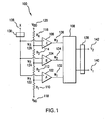
- FIG. 1 is a block diagram of an exemplary conventional two-bit flash ADC 100.
- ADC 100 comprises a first comparator "A” 102, a second comparator “B” 104, a third comparator “C” 106, a priority encoder 108, a first resistor “R 1 " 110, a second resistor “R 2 " 112, a third resistor “R 3 " 114, and a fourth resistor “R 4 " 116.
- Each of R 1 110, R 2 112, R 3 114, and R 4 116 has the same measure of resistance.
- R 1 110, R 2 112, R 3 114, and R 4 116 are connected in series between an analog ground “V AG " 118 and a first supply voltage "V DD " 120.
- analog ground V AG 118 can be replaced by a second supply voltage "V SS ".)
- R 1 110 is connected between V AG 118 and a first node "N 1 " 122.
- R 2 112 is connected between N 1 122 and a second node “N 2 " 124.
- R 3 114 is connected between N 2 124 and a third node “N 3 " 126.
- R 4 116 is connected between N 3 126 and V DD 120.
- the voltage at N 1 122 (the reference voltage of comparator A 102) is equal to V DD /4
- the voltage at N 2 124 (the reference voltage of comparator B 104) is equal to V DD /2
- the voltage at N 3 126 (the reference voltage of comparator C 106) is equal to 3V DD /4.
- comparators A 102, B 104, and C 106 are connected to, respectively, N 1 122,N 2 124, and N 3 126.
- An analog signal "x" 128 is received at an input 130, which is connected to the noninverting terminals of comparators A 102, B 104, and C 106.
- a quantized signal is produced at the output terminal of each comparator.
- Quantized signals "w 1 " 132, "w 2 " 134, and "w 3 " 136 are produced at the output terminals of, respectively, comparators A 102, B 104, and C 106.
- Each quantized signal has a voltage with a value "LOW” or a value "HIGH” depending upon whether a corresponding value of the voltage of analog signal x 128 is less than (or equal to) or greater than the voltage at the inverting terminal of the corresponding comparator (i.e., the reference voltage of the comparator). For example, when the value of the voltage of analog signal x 128 is less than or equal to V DD /4, the values of the voltages of w 3 136, w 2 134, and w 1 132 are equal to, respectively, LOW, LOW, and LOW.
- comparators A 102, B 104, and C 106 are connected to priority encoder 108.
- Quantized signals w 1 132, w 2 134, and w 3 136 are received by priority encoder 108, which processes them to produce, at an output 138, a two-bit digital signal "y” comprising a least significant bit (LSB) signal “y 1 " 140 and a most significant bit (MSB) signal "y 2 " 142.
- LSB least significant bit
- MSB most significant bit
- flash ADC 100 can be modified so that digital signal y comprises more than two bit signals.
- flash ADC 100 can be modified so that digital signal y comprises one bit signal.
- FIG. 2 is a schematic diagram of an exemplary conventional current-mode latch circuit 200 that can be used in an implementation of any of comparators A 102, B 104, or C 106.
- Latch circuit 200 comprises a cross-connected pair of transistors 202 connected between a reset switch 204 and first supply voltage V AG 118.
- cross-connected pair 202 comprises a first NMOSFET (n-channel Metal Oxide Semiconductor Field Effect Transistor) "M 1 " 206 and a second NMOSFET "M 2 " 208.
- M 1 206 and M 2 208 are matched transistors.
- each of M 1 206 and M 2 208 has a gain greater than one.
- cross-connected pair 202 can function if the product of the individual gains of M 1 206 and M 2 208 (i.e., the loop gain) is greater than one.
- the gate terminal of M 2 208 is connected to the drain terminal of M 1 206 at a first port "N 4 " 210.
- the gate terminal of M 1 206 is connected to the drain terminal of M 2 208 at a second port "N 5 " 212.
- the source terminals of M 1 206 and M 2 208 are together connected to analog ground V AG 118.
- reset switch 204 comprises a third NMOSFET "M 3 " 214.
- the source terminal of M 3 214 is connected to the drain terminal of one of M 1 206 or M 2 208; the drain terminal of M 3 214 is connected the drain terminal of the other of M 1 206 or M 2 208.
- a clock waveform "Ck" 216 is applied to the gate terminal of M 3 214. Ck 216 cycles between an "UP” voltage and an “DOWN” voltage at a sampling frequency.
- M 1 206, M 2 208, and M 3 214 can also be realized in other field effect, junction, or combination transistor technologies.
- reset switch 204 can be realized in a variety of switch technologies, including microelectromechanical embodiments.
- Latch circuit 200 can also be used for other applications.
- quantized signal "w” (e.g., w 1 132, w 2 134, or w 3 136) is produced as an output voltage at N 4 210 or N 5 212.
- Latch circuit 200 is often preceded by an input stage (not shown) that includes a differential amplifier so that the voltage of analog signal x 128, applied at the noninverting terminal of the comparator, can be compared with the voltage at the inverting terminal of the comparator.
- the voltage of analog signal x 128 is compared with V DD /4, for comparator A 102; V DD /2, for comparator B 104; and 3V DD /4, for comparator C 106.
- the input stage produces a differential current signal comprising a first current signal "i 1 " 218 and a second current signal “i 2 " 220.
- First and second current signals i 1 218 and i 2 220 each comprise a bias current "i b " and a signal current "i s ".
- first and second current signals i 1 218 and i 2 220 always change currents in opposite directions, but the sum of first and second current signals i 1 218 and i 2 220 remains equal to twice the bias current i b .
- the differential amplifier is configured so that no signal current i s is produced when the voltage of analog signal x 128, applied at the noninverting terminal of the comparator, equals the voltage at the inverting terminal of the comparator.
- no signal current is produced when the voltage of analog signal x 128 equals V DD /4
- comparator B 104 no signal current i s is produced when the voltage of analog signal x 128 equals V DD /2
- comparator C 106 no signal current is is produced when the voltage of analog signal x 128 equals 3V DD /4.
- first current signal i 1 218 and second current signal i 2 220 are received as input current signals at, respectively, N 4 210 and N 5 212.
- M 3 214 connects N 4 210 with N 5 212, so that the steady state voltages at both nodes are equal, and bias current i b flows through each of M 1 206 and M 2 208.
- Parasitic capacitances at each of nodes N 4 210 and N 5 212 are charged by bias current i b that flows through each of M 1 206 and M 2 208.
- the parasitic capacitance at, for example, N 4 210 includes the gate-to-source capacitance of M 2 208, the drain-to-substrate capacitance of M 1 206, the drain-to-substrate capacitance of M 3 214, and the capacitance of the wiring connecting circuit devices.
- Bias current i b charges the parasitic capacitances at each of nodes N 4 210 and N 5 212 so that the voltages at N 4 210 and N 5 212 are at a metastable "MID" value that is between LOW and HIGH.
- the gate and drain terminals of M 1 206 and M 2 208 are connected together.
- M 1 206 and M 2 208 are sized so that, under these conditions, they operate in "ON" states.
- the states of M 1 206 and M 2 208 are controlled by first and second current signals i 1 218 and i 2 220.
- first current signal i 1 218 is greater than bias current i b and second current signal i 2 220 is less than bias current i b
- a transient is initiated to force M 1 206 to operate in an "OFF" state, while M 2 208 remains operating in an ON state.
- the course of this transient depends on how first and second current signals i 1 218 and i 2 220 change during the sampling phase.
- latch circuit 200 It is a characteristic of latch circuit 200 that the port (i.e., N 4 210 or N 5 212) receiving the current signal (i.e., i 1 218 or i 2 220) that is greater than bias current i b requires more time to reach its new steady state voltage than the port receiving the current signal that is less than bias current i b .
- first and second current signals i 1 218 and i 2 220 both have values near to that of bias current i b (i.e., small signal current i s ), it is possible that the output voltage (at N 4 210 or N 5 212) may not reach LOW or HIGH before the end of the sampling phase, but remain in a metastable condition.
- Bit errors can be reduced by increasing bias current i b so that only a small signal current i s is needed to force the port (i.e., N 4 210 or N 5 212) receiving the current signal (i.e., i 1 218 or i 2 220) that is greater than bias current i b to reach its new steady state voltage.
- This increases the overall speed of latch circuit 200.
- increasing bias current i b can decrease the signal-to-noise ratio of ADC 100.
- increasing bias current i b in all of the comparators of ADC 100 causes ADC 100 to dissipate more power, particularly because each comparator draws twice the bias current i b during both the sampling and the reset phases.
- WO 96/37962 describes an analog-to-digital converter, wherein an analog comparator compares an analog signal to be converted with an analog ramp signal. The output of the comparator enables a digital latch having a binary Gray code counter input. When the analog ramp equals the analog signal the digital latch captures the state of the Gray code counter. Metastability in the digital latch is resolved by a latch train.
- the present invention relates to high speed, low power comparators.
- the present invention provides a technique to identify which comparator is in a metastable condition, and to increase the rate at which the identified comparator transitions to a steady state.
- a bias current is provided to the identified comparator in the metastable condition, such that the rate at which the comparator in the metastable condition transitions to the steady state is increased.
- FIG. 1 is a block diagram of an exemplary conventional two-bit flash ADC 100.
- FIG. 2 is a schematic diagram of an exemplary conventional current-mode latch circuit 200 that can be used in an implementation of any of comparators A 102, B 104, or C 106.
- FIG. 3 is a block diagram of an array 300 of current-mode comparators configured in the manner of an embodiment of the present invention.
- FIG. 4A is a schematic diagram of an input stage 400 that can be used with latch circuit 200 in an implementation of any of comparators A 102, B 104, or C 106.
- FIG. 4B is a schematic diagram of an input stage 450 that can be used with latch circuit 200 in an implementation of any of comparators A 102, B 104, or C 106.
- FIG. 5 is a block diagram of a portion of an array 500 of current-mode comparators configured in the manner of another embodiment of the present invention.
- FIG. 6 is a block diagram of a portion of an array 600 of current-mode comparators configured in the manner of yet another embodiment of the present invention.
- FIG. 7 is a schematic diagram of another current-mode latch circuit 700 that can be used in a realization of a comparator of the present invention.
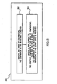
- FIG. 8 shows a flow chart of a method 800 for increasing, in an array of comparators, a rate at which a comparator in a metastable condition transitions to a steady state.
- FIG. 9 shows a flow chart of a preferred method to identify the comparator in the metastable condition.
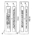
- FIG. 10 shows a flow chart of a method 1000 for increasing, in an array of comparators that includes a first, a second, and a third comparator, a rate at which the third comparator transitions to a steady state.
- the present invention relates to high speed, low power comparators.
- a functional component of a system - such as, but not limited to, a pipelined, subranging, folding, or flash ADC - uses an array of comparators
- the present invention provides a technique to identify which comparator is in a metastable condition, and to increase the rate at which the identified comparator transitions to a steady state.
- FIG. 3 is a block diagram of an array 300 of current-mode comparators configured in the manner of an embodiment of the present invention.
- Array 300 comprises comparator A 102, comparator B 104, comparator C 106, an Exclusive OR gate "XOR” 302, and a variable current source "I v " 304.
- Quantized signals w 1 132 and w 3 136 are received as inputs to XOR 302.
- XOR 302 produces a logic signal "s" 306 that controls variable current source I v 304.
- Variable current source I v 304 augments bias current i b for the latch circuit associated with second comparator B 104 in response to the value of logic signal s 306.
- logic signal s 306 equals one only if quantized signals w 1 132 and w 3 136 have different values. If quantized signals w 1 132 and w 3 136 have the same values, then logic signal s 306 equals zero. For example, when the values of the voltages of w 1 132 and w 3 136 are equal to, respectively, LOW and LOW, then logic signal s 306 is zero. When the values of the voltages of w 1 132 and w 3 136 are equal to, respectively, LOW and HIGH, then logic signal s 306 is one. When the values of the voltages of w 1 132 and w 3 136 are equal to, respectively, HIGH and LOW, then logic signal s 306 is one.
- the present invention is based on the likelihood that, for example, comparator B 104 will be in a metastable condition when comparator A 102 produces quantized signal w 1 132 with value HIGH and comparator C 106 produces quantized signal w 3 136 with value LOW.
- logic signal s 306 is one and, in response, variable current source I v 304 augments bias current i b for the latch circuit associated with comparator B 104.
- bias current i b increases both first and second current signals i 1 218 and i 2 220 and decreases the time needed for the port (i.e., N 4 210 or N 5 212) receiving the current signal (i.e., i 1 218 or i 2 220) that is greater than bias current i b to reach its new steady state voltage. This decreases the probability that comparator B 104 will remain in a metastable condition and thus reduces the bit error rate (BER).
- BER bit error rate
- comparator B 104 if analog signal x 128 is nearly equal to V DD /2, then a small signal current is is produced for comparator B 104, a large positive signal current i s is produced for comparator A 102, and a large negative signal current is is produced for comparator C 106.
- comparator A 102 quickly produces quantized signal w 1 132 with value HIGH
- comparator C 106 quickly produces quantized signal w 3 136 with value LOW
- comparator B 104 may be slow to produce a digital value for quantized signal w 2 134 before the end of the sampling phase.
- Increasing bias current i b to the latch circuit associated with comparator B 104 increases its overall speed, decreases the likelihood that it will remain in a metastable state, and reduces the BER.
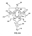
- FIG. 4A is a schematic diagram of an input stage 400 that can be used with latch circuit 200 in an implementation of any of comparators A 102, B 104, or C 106.
- Input stage 400 receives analog signal x 128 and produces first and second current signals i 1 218 and i 2 220, which are received by latch circuit 200.
- Input stage 400 comprises amplifying MOSFETs "M 4 " 402 and "M 5 " 404, load MOSFETs "M 6 " 406 and “M 7 “ 408, current mirror MOSFETs "M 8 " 410 and "M 9 " 412, and variable current source 304.
- Amplifying MOSFETs M 4 402 and M 5 404 are configured as a differential pair with their source terminals connected together.
- a load MOSFET is connected to the drain terminal of each amplifying MOSFET.
- the drain terminal of M 6 406 is connected to the drain terminal of M 4 402; the drain terminal of M 7 408 is connected to the drain terminal of M 5 404.
- the source terminals of M 6 406 and M 7 408 are together connected to first supply voltage V DD 120.
- the source terminals of current mirror MOSFETs M 8 410 and M 9 412 are also together connected to first supply voltage V DD 120.
- M 4 402 and M 5 404 are NMOSFETs
- M 6 406, M 7 408, M 8 410, and M 9 412 are PMOSFETs (p-channel MOSFETs).
- this configuration can be reversed depending upon the overall configuration of the comparator associated with latch circuit 200.
- M 4 402, M 5 404, M 6 406, M 7 408, M 8 410, and M 9 412 can also be realized in other field effect, junction, or combination transistor technologies.
- the voltage of analog signal x 128 is received by input stage 400 at the noninverting terminal of the comparator (e.g., A 102, B 104, or C 106). This allows the voltage of analog signal x 128 to be compared with a reference voltage "ref' 414 received at the inverting terminal of the comparator. For example, the voltage of analog signal x 128 is compared with V DD /4, for comparator A 102; V DD /2, for comparator B 104; and 3 V DD /4, for comparator C 106.
- the noninverting terminal of the comparator is connected to the gate terminal of M 4 402.
- the inverting terminal of the comparator is connected to the gate terminal of M 5 404.
- Amplifying MOSFETs M 4 402 and M 5 404 act to control the distribution of current provided by variable current source I v 304.
- the sum of the current flowing through both M 4 402 and M 5 404 equals the current provided by variable current source I v 304, which is equal to twice bias current i b .
- M 8 410 mirrors the increase in current flowing through M 6 406 to produce first current signal i 1 218 at the drain terminal of M 8 410.
- M 9 412 mirrors the decrease in current flowing through M 7 408 to produce second current signal i 2 220 at the drain terminal of M 9 412.
- Variable current source I v 304 is controlled by Exclusive OR gate XOR 302.
- logic signal s 306 produced by Exclusive OR gate XOR 302 is one, the current produced by variable current source I v 304 is increased, which increases bias current i b for latch circuit 200.
- Increasing bias current i b increases both first and second current signals i 1 218 and i 2 220 and decreases the time needed for the port (i.e., N 4 210 or N 5 212) receiving the current signal (i.e., i 1 218 or i 2 220) that is greater than bias current i b to reach its new steady state voltage. This increases the overall speed of latch circuit 200 and decreases the likelihood that it will remain in a metastable state.
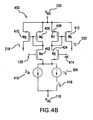
- FIG. 4B is a schematic diagram of an input stage 450 that can be used with latch circuit 200 in an implementation of any of comparators A 102, B 104, or C 106.
- Input stage 450 is configured in the same manner as input stage 400 except that: (1) a fixed current source "2i b " 416 is connected in parallel with variable current source I v 304 between the source terminal of M 4 402 and M 5 404 and analog ground V AG 118, and (2) a switch "S" 418 is connected in series with variable current source I v 304 between the source terminal of M 4 402 and M 5 404 and analog ground V AG 118.
- Fixed current source 2i b 416 produces a current that is equal to twice bias current i b .
- Switch S 418 is controlled by Exclusive OR gate XOR 302. When logic signal s 306 produced by Exclusive OR gate XOR 302 is zero, switch S 418 is opened; when logic signal s 306 produced by Exclusive OR gate 302 is one, switch S 418 is closed. When switch S 418 is closed, the sum of the current flowing through both M 4 402 and M 5 404 equals the current provided by the sum of fixed current source 2i b 416 and variable current source I v 304.
- This sum current increases both first and second current signals i 1 218 and i 2 220 and decreases the time needed for the port (i.e., N 4 210 or N 5 212) receiving the current signal (i.e., i 1 218 or i 2 220) that is greater than bias current i b to reach its new steady state voltage. This increases the overall speed of latch circuit 200 and decreases the likelihood that it will remain in a metastable state.
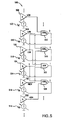
- FIG. 5 is a block diagram of a portion of an array 500 of current-mode comparators configured in the manner of another embodiment of the present invention.
- the portion of array 500 comprises a comparator "O" 502, comparator A 102, comparator B 104, comparator C 106, a comparator “D” 504, a comparator “E” 506, an Exclusive OR gate “XOR A “ 508, Exclusive OR gate XOR 302, an Exclusive OR gate “XOR C “ 510, an Exclusive OR gate “XOR D " 512, a variable current source "I vO “ 514, a variable current source "I vA “ 516, variable current source I v 304, a variable current source "I vC “ 518, a variable current source “I vD “ 520, and a variable current source " I've “ 522.
- the comparators, Exclusive OR gates, and variable current sources of portion of array 500 are configured such that an Exclusive OR gate produces a logic signal that controls a variable current source that augments bias current for a latch circuit of a comparator of the array.
- the Exclusive OR gate receives as inputs quantized signals from other comparators of the array that are adjacent on either side of the bias current augmented comparator.
- the portion of array 500 expands upon the teachings of array 300 to show how the present invention operates in an environment of multiple Exclusive OR gates.
- comparator B 104 may be slow to produce a digital value for its quantized signal before the end of the sampling phase.
- XOR A 508 which receives inputs from comparators O 502 and B 104, does not produce a digital output
- XOR 302 which receives inputs from comparators A 102 and C 106, produces a digital output of one
- XOR C 510 which receives its input from comparators B 104 and D 504, does not produce a digital output
- XOR D 512 which receives inputs from comparators C 106 and E 506, produces a digital output of zero.
- XOR 302 acts to cause variable current source I v 304 to augment bias current i b for the latch circuit associated with comparator B 104.
- comparator B 104 transitions to a new steady state of, for example, HIGH, then XOR A 508 produces a digital output of zero, and XOR C 510 produces a digital output of one.
- XOR C 510 acts to cause variable current source I VC 518 to augment bias current i b for the latch circuit associated with comparator C 106.
- the remaining Exclusive OR gates do not cause their respective variable current sources to augment the bias currents for the latch circuits associated with their comparators.
- FIG. 6 is a block diagram of a portion of an array 600 of current-mode comparators configured in the manner of yet another embodiment of the present invention.
- the portion of array 600 comprises comparator O 502, comparator A 102, comparator B 104, comparator C 106, comparator D 504, comparator E 506, an Exclusive OR gate “XOR AB " 602, an Exclusive OR gate “XOR BC “ 604, an Exclusive OR gate “XOR CD “ 606, variable current source I vO 514, variable current source I vA 516, variable current source I v 304, variable current source I vC 518, variable current source I vD 520, and variable current source I've 522.
- the portion of array 600 expands upon the teachings of array 500 to show how the present invention can provide the designer with a tradeoffbetween power dissipated and die area consumed.
- XOR AB 602 receives inputs from comparators O 502 and C 106, and controls variable current sources I vA 516 and I v 304;
- XOR BC 604 receives inputs from comparators A 102 and D 504, and controls variable current sources I v 304 and I vC 518;
- XOR CD 606 receives inputs from comparators B 104 and E 506, and controls variable current sources I vC 518 and I vD 520.
- comparator B 104 may be slow to produce a digital value for its quantized signal before the end of the sampling phase.
- XOR AB 602 produces a digital output of one
- XOR BC 604 produces a digital output of one
- XOR CD 606 does not produce a digital output.
- XOR AB 602 and XOR BC 604 act to cause variable current sources I vA 516, I v 304, and I vC 518 to augment bias currents i b for the latch circuits associated with comparators A 102, B 104, and C 106.
- XOR CD 606 acts to cause variable current source I VD 520 to augments bias current i b for the latch circuit associated with comparator D 504.
- array 600 draws more current (and hence dissipates more power) than array 500.
- array 600 consumes less die area than array 500.
- FIG. 7 is a schematic diagram of another current-mode latch circuit 700 that can be used in a realization a comparator of the present invention.
- Latch circuit 700 comprises latch circuit 200, a first vertical latch 702 with a first vertical latch reset switch 704, a second vertical latch 706 with a second vertical latch reset switch 708, and a second pair of cross connected transistors 710.
- First vertical latch 702 is connected between analog ground V AG 118 and first supply voltage V DD 120.
- first vertical latch 702 comprises a fourth NMOSFET "M 10 " 712 and a first PMOSFET "M 11 " 714.
- each of M 10 712 and M 11 714 has a gain greater than one.
- first vertical latch 702 can function if the product of the individual gains of M 10 712 and M 11 714 (i.e., the loop gain) is greater than one.
- the source terminal of M 10 712 is connected to analog ground V AG 118.
- the drain terminal of M 10 712 is connected to the gate terminal of M 11 714.
- the gate terminal of M 10 712 is connected to the gate terminal of M 2 208.
- the source terminal of M 11 714 is connected to first supply voltage V DD 120.
- the drain terminal of M 11 714 is connected to the gate terminal of M 10 712.
- M 10 712 and M 11 714 can also be realized in other field effect, junction, or combination transistor technologies.
- first vertical latch reset switch 704 comprises a second PMOSFET "M 12 " 716.
- the source terminal of M 12 716 is connected to first supply voltage V DD 120.
- the drain terminal of M 12 716 is connected to the gate terminal of M 11 714.
- An inverse clock waveform "Ck.bar” 718 is applied to the gate terminal of M 12 716.
- Ck.bar 718 cycles between DOWN voltage and UP voltage at the sampling frequency in a manner such that when the voltage of Ck 216 is UP, the voltage of Ck.bar 718 is DOWN, and vice versa.
- M 12 716 can also be realized in other field effect, junction, or combination transistor technologies.
- first vertical latch reset switch 704 can be realized in a variety of switch technologies, including microelectromechanical embodiments.
- Second vertical latch 706 is connected between analog ground V AG 118 and first supply voltage V DD 120.
- second vertical latch 706 comprises a fifth NMOSFET "M 13 " 720 and a third PMOSFET "M 14 " 722.
- each of M 13 720 and M 14 722 has a gain greater than one.
- second vertical latch 706 can function if the product of the individual gains of M 13 720 and M 14 722 (i.e., the loop gain) is greater than one.
- the source terminal of M 13 720 is connected to analog ground V AG 118.
- the drain terminal of M 13 720 is connected to the gate terminal of M 14 722.
- the gate terminal of M 13 720 is connected to the gate terminal of M 1 206.
- the source terminal of M 14 722 is connected to first supply voltage V DD 120.
- the drain terminal of M 14 722 is connected to the gate terminal of M 13 720.
- M 13 720 and M 14 722 can also be realized in other field effect, junction, or combination transistor technologies.
- second vertical latch reset switch 708 comprises a fourth PMOSFET "M 15 " 724.
- the source terminal of M 15 724 is connected to first supply voltage V DD 120.
- the drain terminal of M 15 724 is connected to the gate terminal of M 14 722.
- Inverse clock waveform Ck.bar 506 is applied to the gate terminal of M 15 724.
- M 13 720, M 14 722, and M 15 724 can also be realized in other field effect, junction, or combination transistor technologies.
- second vertical latch reset switch 708 can be realized in a variety of switch technologies, including microelectromechanical embodiments.
- second cross connected pair 710 comprises a fifth PMOSFET "M 16 " 726 and a sixth PMOSFET "M 17 " 728, where M 16 726 and M 17 728 are matched transistors.
- each of M 16 726 and M 17 728 has a gain greater than one.
- second cross connected pair 710 can function if the product of the individual gains of M 16 726 and M 17 728 (i.e., the loop gain) is greater than one.
- the gate terminal of M 17 728 is connected to the drain terminal of M 16 726 and to the gate terminal of M 14 722.
- the gate terminal of M 16 726 is connected to the drain terminal of M 17 728 and to the gate terminal of M 11 714.
- the source terminals of M 16 726 and M 17 728 are together connected to first supply voltage V DD 120.
- M 16 726 and M 17 728 can also be realized in other field effect, junction, or combination transistor technologies.
- First vertical latch 702 and second vertical latch 706 act to increase the rate at which the port (i.e., N 4 210 or N 5 212) receiving the current signal (i.e., i 1 218 or i 2 220) that is greater than bias current i b reaches its new steady state voltage.
- first and second current signals i 1 218 and i 2 220 are controlled by first and second current signals i 1 218 and i 2 220. If first current signal i 1 218 is greater than bias current i b , first current signal i 1 218 continues to charge the parasitic capacitances at N 4 210, which causes the voltage at N 4 210 to rise. Contemporaneously, when second current signal i 2 220 is less than bias current i b , the parasitic capacitances at N 5 212 start to discharge, which causes the voltage at N 5 212 to drop.
- the voltage at N 5 212 is also the voltage at the gate terminal of M 1 206
- the voltage at the gate terminal of M 1 206 drops by the same amount as the drop in the voltage at N 5 212.
- the gate-to-source voltage of M 1 206 decreases by the same amount as the drop in the voltage at the gate terminal of M 1 206.
- the decrease in the gate-to-source voltage of M 1 206 causes its drain current to decrease.
- the drain-to-source voltage of M 1 206 increases by a greater magnitude than the decrease in its gate-to-source voltage.
- the voltage at N 4 210 is also the voltage at the gate terminal of M 2 208, the voltage at the gate terminal of M 2 208 rises by the same amount as the rise in the voltage at N 4 210.
- the voltage at N 4 210 is also the voltage at the gate terminal of M 10 712, the voltage at the gate terminal of M 10 712 rises by the same amount as the rise in the voltage at N 4 210.
- the gate-to-source voltage of M 2 208 increases by the same amount as the rise in the voltage at the gate terminal of M 2 208.
- the increase in the gate-to-source voltage of M 2 208 causes its drain current to increase.
- the drain-to-source voltage of M 2 208 decreases by a greater magnitude than the increase in its gate-to-source voltage.
- the gate-to-source voltage of M 10 712 increases by the same amount as the rise in the voltage at the gate terminal of M 10 712.
- the increase in the gate-to-source voltage of M 10 712 causes its drain current to increase.
- the drain-to-source voltage of M 10 712 decreases by a greater magnitude than the increase in its gate-to-source voltage.
- the decrease in the drain-to-source voltage of M 10 712 causes the voltage at the drain terminal of M 10 712 to drop by the same amount. Because the voltage at the drain terminal of M 10 712 is also the voltage at the gate terminal of M 11 714, the voltage at the gate terminal of M 11 714 drops by the same amount as the drop in the voltage at the drain terminal of M 10 712. Because the voltage at the source terminal of M 11 714 is held at first supply voltage V DD 120, the drop in the voltage at the gate terminal of M 11 714 (i.e., a PMOSFET) causes its source-to-gate voltage to increase by the same amount.
- a PMOSFET causes its source-to-gate voltage to increase by the same amount.
- the increase in the source-to-gate voltage of M 11 714 causes its drain current to increase.
- the source-to-drain voltage of M 11 714 decreases by a greater magnitude than the increase in its source-to-gate voltage.
- the voltage at the source terminal of M 2 208 is held at analog ground V AG 118, the voltage at N 5 212 drops by the same amount as the decrease in drain-to-source voltage of M 2 208.
- the voltage at N 5 212 drops under the relatively small effect of second current signal i 2 220 being less than bias current i b , and the relatively large effect of the decrease in the drain-to-source voltage of M 2 208.
- the voltage at N 4 210 is also the voltage at the drain terminal of M 11 714 and because the voltage at the source terminal of M 11 714 is held at first supply voltage V DD 120, the voltage at N 4 210 rises by the same amount as the decrease in the source-to-drain voltage of M 11 714. Furthermore, because the voltage at the source terminal of M 1 206 is held at analog ground V AG 118, the voltage at N 4 210 rises by the same amount as the increase in drain-to-source voltage of M 1 206.
- the voltage at N 4 210 rises under the relatively small effect of first current signal i 1 218 being greater than bias current i b , the relatively large effect of the increase in the drain-to-source voltage of M 1 206, and the relatively larger effect of the decrease in the source-to-drain voltage of M 11 714.
- the gate-to-source voltage of M 1 206 decreases with the source-to-drain voltage of M 2 208 until M 1 206 is turned OFF.
- M 1 206 When M 1 206 is OFF, it does not conduct current. Without drain current, the decreasing of the gate-to-source voltage of M 1 206 no longer effects its drain-to-source voltage. However, the voltage at N 4 210 continues to rise under the relatively small effect of first current signal i 1 218 being greater than bias current i b and the relatively larger effect of the decrease in the source-to-drain voltage of M 11 714 until the parasitic capacitances at N 4 210 are fully charged and the voltage at N 4 210 is HIGH.
- M 10 712 and M 11 714 form a positive feedback loop that amplifies first current signal i 1 218 and applies an exponentially growing current to the drain terminal of M 1 206.
- the parasitic capacitances at N 4 210 are charged under the combined effects of first current signal i 1 218 and the exponentially growing current drawn from first supply voltage V DD 120 by M 11 714.
- First vertical latch reset switch 704 and second vertical latch reset switch 708 act to reduce the power dissipated by, respectively, first vertical latch 702 and second vertical latch 706 during the reset phase.
- M 12 716 i.e., a PMOSFET
- M 11 714 connects the gate terminal of M 11 714 to first supply voltage V DD 120.
- the gate-to-source voltage of M 11 714 is made to equal zero, holding M 11 714 OFF. This disrupts the latching action of first vertical latch 702 so that cross connected pair 202 can assume a state independent of the state of first vertical latch 702.
- the source-to-gate voltages of M 12 716 and M 15 724 can drift to values greater than their threshold voltages such that M 11 714 and M 14 722 turn ON.
- M 1 206, M 2 208, M 10 712, M 11 714, M 13 720, and M 14 722 all ON before the MOSFETs change states can cause latch circuit 700 to draw a large amount of current.
- Latch circuit 700 acts, in response to first and second current signals i 1 218 and i 2 220, to force one MOSFET of second cross connected pair 710 (e.g., M 16 726) ON while the other MOSFET of second cross connected pair 710 (e.g., M 17 728) remains OFF.
- the MOSFET of second cross connected pair 710 e.g., M 16 726) that turns ON connects the gate terminal of its corresponding vertical latch MOSFET (e.g., M 14 722) to first supply voltage V DD 120. With the gate and source terminals of the corresponding vertical latch MOSFET connected together, the gate-to-source voltage of the corresponding vertical latch MOSFET is made to equal zero, holding the corresponding vertical latch MOSFET OFF. In this manner, second cross connected pair 710 acts to prevent latch circuit 700 from drawing unnecessary current before the MOSFETs change states during the sampling phase.
- first current signal i 1 218 when, at the start of the sampling phase, first current signal i 1 218 is slightly larger than bias current i b (i.e., small positive signal current i s ), then first current signal i 1 218 slowly continues to charge the parasitic capacitances at N 4 210, which causes the voltage at N 4 210 to rise slightly. Because the voltage at N 4 210 is also the voltage at the gate terminal of M 10 712, the voltage at the gate terminal of M 10 712 rises by the same amount as the rise in the voltage at N 4 210.
- bias current i b i.e., small positive signal current i s
- the gate-to-source voltage of M 10 712 increases by the same amount as the rise in the voltage at the gate terminal of M 10 712.
- the increase in the gate-to-source voltage of M 10 712 causes its drain current to increase.
- the drain-to-source voltage of M 10 712 decreases by a greater magnitude than the increase in its gate-to-source voltage. Because the voltage at the source terminal of M 10 712 is held at analog ground V AG 118, the decrease in the drain-to-source voltage of M 10 712 causes the voltage at the drain terminal of M 10 712 to drop by the same amount.
- the voltage at the drain terminal of M 10 712 is also the voltage at the gate terminal of M 16 726, the voltage at the gate terminal of M 16 726 drops by the same amount as the drop in the voltage at the drain terminal of M 10 712.
- the drop in the voltage at the gate terminal of M 16 726 causes its source-to-gate voltage to increase by the same amount.
- the increase in the source-to-gate voltage of M 16 726 causes its drain current to increase.
- the source-to-drain voltage of M 16 726 decreases by a greater magnitude than the decrease in its source-to-gate voltage.
- the decrease in the source-to-drain voltage of M 16 726 causes the voltage at the drain terminal of M 16 726 to rise by the same amount.
- the voltage at the drain terminal of M 16 726 is also the voltage at the gate terminal of M 14 722
- the voltage at the gate terminal of M 14 722 rises by the same amount as the rise in the voltage at the drain terminal of M 16 726.
- the voltage at the source terminal of M 14 722 is held at first supply voltage V DD 120
- the rise in the voltage at the gate terminal of M 14 722 causes its source-to-gate voltage to decrease by the same amount.
- the decrease in the source-to-gate voltage of M 14 722 ensures that it is less than its threshold voltage so that M 14 722 is held OFF. Having M 14 722 held OFF until first current signal i 1 218 charges the parasitic capacitances at N 4 210 to its new steady state voltage of HIGH prevents latch circuit 700 from drawing unnecessary current during the sampling phase.
- latch circuit 700 For an ADC that incorporates an array of comparators based on latch circuit 700, in which the parameters that define latch circuit 700 (i.e., supply voltages, clock frequency, etc.) had specific values, where the ADC was configured with Exclusive OR gates in the manner of the present invention, simulation showed an improvement in the BER from 10 -50 to 10 -100 .
- Latch circuit 700 is further described in Application No. 10/083,463, filed on February 27, 2002, which is incorporated herein by reference.
- FIG. 8 shows a flow chart of a method 800 for increasing, in an array of comparators, a rate at which a comparator in a metastable condition transitions to a steady state.
- the comparator in the metastable condition in the array of comparators is identified.
- a bias current is provided to the identified comparator in the metastable condition, such that the rate at which the comparator in the metastable condition transitions to the steady state is increased.
- the bias current is provided by controlling a current output from a variable current source that provides the bias current for a latch circuit of the identified comparator in the metastable condition.
- FIG. 9 shows a flow chart of a preferred method to identify the comparator in the metastable condition.
- a characteristic of a first comparator of the array of comparators is compared with a characteristic of a second comparator of the array of comparators.
- the first comparator and the second comparator are separated in the array of comparators by a third comparator in the array of comparators.
- the characteristics are compared by receiving the characteristics as inputs to an Exclusive OR gate.
- the bias current is provided by controlling a current output from a variable current source that provides the bias current for a latch circuit of the identified comparator in the metastable condition with an output of an Exclusive OR gate.
- the bias current is provided by connecting a first current source in parallel with a second current source to increase the bias current for a latch circuit of the identified comparator in the metastable condition.
- a switch that connects the first current source in parallel with the second current source is controlled by an output of an Exclusive OR gate.
- FIG. 10 shows a flow chart of a method 1000 for increasing, in an array of comparators that includes a first, a second, and a third comparator, a rate at which the third comparator transitions to a steady state.
- a step 1002 an output of the first comparator is compared with an output of the second comparator.
- a bias current is provided to the third comparator.
- the outputs are compared by receiving the first and second outputs as inputs to an Exclusive OR gate.
- a variable current source that provides the bias current for a latch circuit of the third comparator is controlled based on an output of an Exclusive OR gate.
- the bias current is provided to the third comparator by connecting a first current source in parallel with a second current source to increase the bias current for a latch circuit of the third comparator.
- a switch that connects the first current source in parallel with the second current source is controlled based on an output of an Exclusive OR gate.
- the bias current is provided by controlling a current output from a variable current source that provides the bias current for a latch circuit of the identified comparator in the metastable condition.
Landscapes
- Engineering & Computer Science (AREA)
- Theoretical Computer Science (AREA)
- Analogue/Digital Conversion (AREA)
Claims (20)
- Réseau de comparateurs, comprenant :un premier comparateur (102), un deuxième comparateur (106) et un troisième comparateur (108) ;une porte OU exclusif (302) ayant une première entrée connectée à une sortie dudit premier comparateur (102) et une seconde entrée connectée à une sortie dudit deuxième comparateur (106) ;caractérisé en ce que
la porte OU exclusif (302) est configurée pour comparer la sortie du premier comparateur (102) à la sortie du deuxième comparateur (106) pour déterminer si le troisième comparateur (104) se trouve dans une condition métastable ;
le réseau de comparateurs comprend en outre une source de courant variable (304) connectée à une sortie de ladite porte OU exclusif (302), ladite source de courant variable (304) fournissant un courant de polarisation au dit troisième comparateur (104) sur la base desdites première et seconde sorties comparées pour accroître un taux auquel le troisième comparateur (104) effectue une transition de la condition métastable à un état stable. - Réseau de comparateurs selon la revendication 1, dans lequel ladite sortie de ladite porte OU exclusif (302) produit un signal (306) qui régule ladite source de courant variable (304).
- Réseau de comparateurs selon la revendication 2, dans lequel ledit courant de polarisation est augmenté par ladite source de courant variable (304) en fonction dudit signal (306).
- Réseau de comparateurs selon la revendication 1, dans lequel ledit troisième comparateur (104) est agencé dans le réseau de comparateurs entre ledit premier comparateur (102) et ledit deuxième comparateur (106).
- Réseau de comparateurs selon la revendication 4, dans lequel la porte OU exclusif (302) est configurée pour :recevoir une caractéristique du premier comparateur (102) à sa première entrée et une caractéristique du deuxième comparateur (106) à sa seconde entrée ;comparer les caractéristiques reçues du premier comparateur (102) et du deuxième comparateur (106) pour déterminer si le troisième comparateur (104) est dans une condition métastable.
- Réseau de comparateurs selon la revendication 1, dans lequel ledit troisième comparateur (104) comprend un circuit de verrou configuré pour recevoir ledit courant de polarisation.
- Réseau de comparateurs selon la revendication 6, dans lequel ledit circuit de verrou comprend une paire en connexion croisée de transistors connectés entre un commutateur de réinitialisation et une tension d'alimentation, et ayant un premier port capable de recevoir un premier signal de courant et de produire une première tension de sortie, et un second port capable de recevoir un second signal de courant et de produire une seconde tension de sortie.
- Réseau de comparateurs selon la revendication 7, dans lequel ladite paire en connexion croisée de transistors comprend :un premier MOSFET ; etun second MOSFET connecté au dit premier MOSFET ;dans lequel :une borne de porte dudit premier MOSFET est connectée à une borne de drain dudit second MOSFET ;une borne de porte dudit second MOSFET est connectée à une borne de drain dudit premier MOSFET ; etdes bornes de source dudit premier MOSFET et dudit second MOSFET sont connectées à ladite tension d'alimentation.
- Réseau de comparateurs selon la revendication 7, dans lequel ledit commutateur de réinitialisation comprend un MOSFET connecté entre ledit premier port et ledit second port.
- Réseau de comparateurs selon la revendication 1, comprenant en outre :une seconde porte OU exclusif (302) ayant une entrée connectée à une sortie dudit troisième comparateur (104) ; etune seconde source de courant variable connectée à une sortie de ladite seconde porte OU exclusif (302), ladite seconde source de courant variable fournissant un second courant de polarisation au dit deuxième comparateur (106).
- Convertisseur analogique numérique comprenant :un réseau de comparateurs selon l'une quelconque des revendications 1 à 10, le réseau de comparateurs ayant des entrées respectives configurées pour recevoir un signal analogique, et des sorties respectives configurées pour produire des signaux quantifiés en réponse au dit signal analogique ;un codeur de priorité connecté au dit réseau de comparateurs, configuré pour produire un signal numérique à une sortie en réponse aux dits signaux quantifiés ;un réseau de portes OU exclusif, dans lequel chaque porte OU exclusif dudit réseau de portes OU exclusif est configurée pour recevoir deux desdits signaux quantifiés ; etun réseau de sources de courant variable, dans lequel chaque source de courant variable dudit réseau de sources de courant variable est configurée pour fournir un courant de polarisation à un comparateur correspondant dudit réseau de comparateurs, et est régulée par une sortie d'une porte OU exclusif correspondante dudit réseau de portes OU exclusif.
- Convertisseur analogique numérique selon la revendication 11, dans lequel chaque porte OU exclusif dudit réseau de portes OU exclusif produit un signal logique qui régule une source de courant variable correspondante dudit réseau de sources de courant variable.
- Convertisseur analogique numérique selon la revendication 11, dans lequel chaque comparateur dudit réseau de comparateurs comprend un circuit de verrou configuré pour recevoir un courant de polarisation correspondant.
- Convertisseur analogique numérique selon la revendication 13, dans lequel ledit courant de polarisation correspondant est capable d'être augmenté par une source de courant variable correspondante dudit réseau de sources de courant variable.
- Procédé pour augmenter un taux auquel un comparateur effectue une transition dans un état constant pour une utilisation dans un réseau de comparateurs qui comprend un premier comparateur (102), un deuxième comparateur (106) et un troisième comparateur (104), une porte OU exclusif (302), et une source de courant variable (304), le procédé comprenant les étapes consistant à :(1) comparer (1002), par la porte OU exclusif (302), une sortie du premier comparateur (102) à une sortie du deuxième comparateur (106) pour déterminer si le troisième comparateur (104) se trouve dans une condition métastable ; et(2) fournir (1004), par la source de courant variable (304), un courant de polarisation au troisième comparateur (104) sur la base desdites première et seconde sorties comparées pour accroître un taux auquel le troisième comparateur (104) effectue une transition de la condition métastable à un état stable.
- Procédé selon la revendication 15, dans lequel ladite étape de comparaison (1002) comprend l'étape consistant à :recevoir les première et seconde sorties en tant qu'entrées sur la porte OU exclusif (302).
- Procédé selon la revendication 16, dans lequel ladite étape de fourniture (1004) comprend l'étape consistant à :réguler la source de courant variable (304) qui fournit le courant de polarisation pour un circuit de verrou du troisième comparateur (104) sur la base d'une sortie de la porte OU exclusif (302).
- Procédé selon la revendication 15, dans lequel la sortie du premier comparateur (102) et la sortie du deuxième comparateur (106) sont comparées par la porte OU exclusif (302) pour déterminer si le troisième comparateur (104) est dans une condition métastable, dans lequel le premier comparateur (102) et le deuxième comparateur (106) sont séparés dans le réseau de comparateurs par le troisième comparateur (104) dans le réseau de comparateurs.
- Procédé selon la revendication 15, dans lequel ladite étape de fourniture (1004) comprend l'étape consistant à :connecter une première source de courant en parallèle à une seconde source de courant pour augmenter le courant de polarisation pour un circuit de verrou du troisième comparateur (104).
- Procédé selon la revendication 19, comprenant en outre l'étape consistant à :commander un commutateur qui connecte la première source de courant en parallèle à la seconde source de courant sur la base d'une sortie de la porte OU exclusif (302).
Applications Claiming Priority (2)
| Application Number | Priority Date | Filing Date | Title |
|---|---|---|---|
| US226165 | 1988-07-29 | ||
| US10/226,165 US6727839B2 (en) | 2002-08-23 | 2002-08-23 | High speed, low power comparator |
Publications (3)
| Publication Number | Publication Date |
|---|---|
| EP1391994A2 EP1391994A2 (fr) | 2004-02-25 |
| EP1391994A3 EP1391994A3 (fr) | 2006-03-22 |
| EP1391994B1 true EP1391994B1 (fr) | 2008-04-23 |
Family
ID=31188013
Family Applications (1)
| Application Number | Title | Priority Date | Filing Date |
|---|---|---|---|
| EP03019212A Expired - Lifetime EP1391994B1 (fr) | 2002-08-23 | 2003-08-25 | Réseau de comparateurs comprenant des moyens pour résolution rapide de métastabilité |
Country Status (3)
| Country | Link |
|---|---|
| US (3) | US6727839B2 (fr) |
| EP (1) | EP1391994B1 (fr) |
| DE (1) | DE60320492T2 (fr) |
Cited By (2)
| Publication number | Priority date | Publication date | Assignee | Title |
|---|---|---|---|---|
| US7906145B2 (en) | 2002-04-09 | 2011-03-15 | Flamel Technologies | Oral pharmaceutical formulation in the form of aqueous suspension for modified release of active principle(s) |
| US7910133B2 (en) | 2002-04-09 | 2011-03-22 | Flamel Technologies | Oral pharmaceutical formulation in the form of aqueous suspension of microcapsules for modified release of amoxicillin |
Families Citing this family (17)
| Publication number | Priority date | Publication date | Assignee | Title |
|---|---|---|---|---|
| US6191719B1 (en) * | 1997-08-25 | 2001-02-20 | Broadcom Corporation | Digital to analog converter with reduced ringing |
| US7161523B1 (en) * | 2004-09-03 | 2007-01-09 | Pmc-Sierra, Inc. | Systems and methods for a self-organizing analog-to-digital converter |
| US8218693B2 (en) * | 2006-03-09 | 2012-07-10 | Broadcom Corporation | Gain control for wireless receiver |
| US8467473B2 (en) * | 2006-03-31 | 2013-06-18 | Broadcom Corporation | Power control techniques for wireless transmitters |
| US8719723B2 (en) * | 2007-03-05 | 2014-05-06 | Microsoft Corporation | Displaying data sensitive targets |
| US7623051B2 (en) * | 2008-04-29 | 2009-11-24 | Analog Devices, Inc. | Metastability error reduction in signal converter systems |
| US7965217B2 (en) * | 2009-10-13 | 2011-06-21 | Analog Devices, Inc. | Apparatus and method for pipelined analog to digital conversion |
| US7978116B2 (en) * | 2009-10-13 | 2011-07-12 | Analog Devices, Inc. | Apparatus and method for pipelined analog to digital conversion |
| US8416106B2 (en) * | 2011-04-20 | 2013-04-09 | Fujitsu Limited | Calibration scheme for resolution scaling, power scaling, variable input swing and comparator offset cancellation for flash ADCs |
| US8878713B1 (en) * | 2013-06-20 | 2014-11-04 | Fujitsu Limited | Crossbar switch calibration system for facilitating analog-to-digital conversion monotonicity |
| US9252751B2 (en) | 2014-05-04 | 2016-02-02 | Freescale Semiconductor, Inc. | Apparatus and method for preventing multiple resets |
| US9329210B1 (en) | 2014-11-29 | 2016-05-03 | Freescale Semiocnductor, Inc. | Voltage monitoring circuit |
| TWI554042B (zh) | 2014-12-08 | 2016-10-11 | 財團法人工業技術研究院 | 訊號比較裝置及其控制方法 |
| CN105897268B (zh) * | 2016-05-12 | 2023-04-28 | 豪威模拟集成电路(北京)有限公司 | 亚稳态消除电路及其设备 |
| CN108494406B (zh) * | 2018-03-23 | 2022-03-18 | 上海唯捷创芯电子技术有限公司 | 一种高速动态锁存型比较器、芯片及通信终端 |
| KR102905976B1 (ko) | 2021-04-23 | 2025-12-29 | 삼성전자 주식회사 | 증폭기 회로 |
| CN119945444B (zh) * | 2025-01-02 | 2025-11-28 | 广东工业大学 | 具有亚稳态检测纠正的五态比较器及五态型量化逐次逼近方法 |
Family Cites Families (19)
| Publication number | Priority date | Publication date | Assignee | Title |
|---|---|---|---|---|
| US3393298A (en) * | 1965-04-01 | 1968-07-16 | Bell Telephone Labor Inc | Double-rank binary counter |
| US4092955A (en) * | 1976-10-04 | 1978-06-06 | The Bendix Corporation | Roughness sensor |
| US4417317A (en) * | 1980-02-04 | 1983-11-22 | Westinghouse Electric Corp. | Adaptive analog processor |
| US5034746A (en) * | 1988-09-21 | 1991-07-23 | International Business Machines Corporation | Analog-to-digital converter for computer disk file servo position error signal |
| JPH0443718A (ja) * | 1990-06-11 | 1992-02-13 | Matsushita Electric Ind Co Ltd | 並列型a/d変換器 |
| US5070332A (en) * | 1991-03-18 | 1991-12-03 | Burr-Brown Corporation | Two-step subranging analog to digital converter |
| JP3318725B2 (ja) * | 1994-01-12 | 2002-08-26 | 株式会社日立製作所 | アナログフィルタ回路 |
| US5621406A (en) * | 1994-09-29 | 1997-04-15 | Rosemount Inc. | System for calibrating analog-to-digital converter |
| US5721503A (en) * | 1994-10-26 | 1998-02-24 | Hughes Aircraft Company | Flash analog-to-digital converter with latching exclusive or gates |
| IL118403A (en) * | 1995-05-25 | 2001-09-13 | Lockheed Martin Ir Imaging Sys | Monolithic analog-digital converter and method for the same |
| US5748132A (en) * | 1995-07-17 | 1998-05-05 | Matsushita Electric Industrial Co., Ltd. | Interpolation type A/D converter |
| KR0174499B1 (ko) * | 1995-10-13 | 1999-04-01 | 김광호 | 비교기의 입력 바이어스전류가 보상된 아날로그 디지탈 변환기 |
| US5764175A (en) * | 1996-09-24 | 1998-06-09 | Linear Technology Corporation | Dual resolution circuitry for an analog-to-digital converter |
| US5825239A (en) * | 1997-05-06 | 1998-10-20 | Texas Instruments Incorporated | Peak detector for automatic gain control |
| JP3450649B2 (ja) | 1997-06-04 | 2003-09-29 | 株式会社東芝 | アナログ/デジタル変換装置 |
| US6091353A (en) * | 1998-07-15 | 2000-07-18 | International Business Machines Corporation | Bias circuit for flash analog to digital converter circuits |
| EP1087507B1 (fr) * | 1999-09-21 | 2004-10-13 | STMicroelectronics S.r.l. | Procédé de contrôle d'un convertisseur continu-continu |
| JP4742455B2 (ja) * | 2001-06-26 | 2011-08-10 | 日本テキサス・インスツルメンツ株式会社 | レギュレータ回路 |
| US6714049B2 (en) * | 2001-08-10 | 2004-03-30 | Shakti Systems, Inc. | Logic state transition sensor circuit |
-
2002
- 2002-08-23 US US10/226,165 patent/US6727839B2/en not_active Expired - Fee Related
-
2003
- 2003-08-25 EP EP03019212A patent/EP1391994B1/fr not_active Expired - Lifetime
- 2003-08-25 DE DE60320492T patent/DE60320492T2/de not_active Expired - Lifetime
-
2004
- 2004-03-12 US US10/798,552 patent/US6876318B2/en not_active Expired - Fee Related
-
2005
- 2005-03-24 US US11/087,685 patent/US7129865B2/en not_active Expired - Fee Related
Cited By (2)
| Publication number | Priority date | Publication date | Assignee | Title |
|---|---|---|---|---|
| US7906145B2 (en) | 2002-04-09 | 2011-03-15 | Flamel Technologies | Oral pharmaceutical formulation in the form of aqueous suspension for modified release of active principle(s) |
| US7910133B2 (en) | 2002-04-09 | 2011-03-22 | Flamel Technologies | Oral pharmaceutical formulation in the form of aqueous suspension of microcapsules for modified release of amoxicillin |
Also Published As
| Publication number | Publication date |
|---|---|
| US20040036644A1 (en) | 2004-02-26 |
| US20040169597A1 (en) | 2004-09-02 |
| US6876318B2 (en) | 2005-04-05 |
| DE60320492D1 (de) | 2008-06-05 |
| EP1391994A2 (fr) | 2004-02-25 |
| US20050162195A1 (en) | 2005-07-28 |
| US6727839B2 (en) | 2004-04-27 |
| DE60320492T2 (de) | 2009-06-10 |
| US7129865B2 (en) | 2006-10-31 |
| EP1391994A3 (fr) | 2006-03-22 |
Similar Documents
| Publication | Publication Date | Title |
|---|---|---|
| EP1391994B1 (fr) | Réseau de comparateurs comprenant des moyens pour résolution rapide de métastabilité | |
| US6037890A (en) | Ultra high speed, low power, flash A/D converter utilizing a current mode regenerative comparator | |
| CN103518327B (zh) | 自定时的数模转换器 | |
| US7199745B2 (en) | Successive approximation A/D converter provided with a sample-hold amplifier | |
| US8723712B1 (en) | Digital to analog converter with current steering source for reduced glitch energy error | |
| US8410820B2 (en) | High speed latch comparators | |
| TWI596907B (zh) | 數位類比轉換器 | |
| JP2006517765A (ja) | 臨界的な連続時間用途における自動ゼロ化 | |
| TWI792438B (zh) | 訊號轉換裝置、動態元件匹配電路與動態元件匹配方法 | |
| US7061421B1 (en) | Flash ADC with variable LSB | |
| US6859158B2 (en) | Analog-digital conversion circuit | |
| US20100289683A1 (en) | Reference voltage generation circuit, a/d converter and d/a converter | |
| Fani et al. | A 1-V 5-bit 0.5 GS/s time-based flash ADC in 0.18 µm CMOS technology | |
| Hamoui et al. | A 1.8-V 3-MS/s 13-bit/spl Delta//spl Sigma/A/D converter with pseudo data-weighted-averaging in 0.18-/spl mu/m digital CMOS | |
| JP2004260263A (ja) | Ad変換器 | |
| US7116261B1 (en) | Method and apparatus for accurate inverse-linear voltage/current generator | |
| Sam et al. | A new architecture of Thermometer to Binary code encoder for 4-bit FLASH ADC in 45nm CMOS process | |
| US11728824B2 (en) | Analog circuit and comparator sharing method of analog circuit | |
| CN115483930B (zh) | 模拟电路与用于模拟电路的比较器共用方法 | |
| Qureshi et al. | Feasibility study of an ultra high speed current-mode sar adc | |
| Yu et al. | Low-power 4-bit flash ADC for digitally controlled DC-DC converter | |
| CN117478144A (zh) | 电容器加权分段缓冲器 | |
| JP2010251986A (ja) | アナログ/デジタル変換器 | |
| JP2007325319A (ja) | アナログ−デジタル変換器 |
Legal Events
| Date | Code | Title | Description |
|---|---|---|---|
| PUAI | Public reference made under article 153(3) epc to a published international application that has entered the european phase |
Free format text: ORIGINAL CODE: 0009012 |
|
| AK | Designated contracting states |
Kind code of ref document: A2 Designated state(s): AT BE BG CH CY CZ DE DK EE ES FI FR GB GR HU IE IT LI LU MC NL PT RO SE SI SK TR |
|
| AX | Request for extension of the european patent |
Extension state: AL LT LV MK |
|
| PUAL | Search report despatched |
Free format text: ORIGINAL CODE: 0009013 |
|
| AK | Designated contracting states |
Kind code of ref document: A3 Designated state(s): AT BE BG CH CY CZ DE DK EE ES FI FR GB GR HU IE IT LI LU MC NL PT RO SE SI SK TR |
|
| AX | Request for extension of the european patent |
Extension state: AL LT LV MK |
|
| 17P | Request for examination filed |
Effective date: 20060922 |
|
| AKX | Designation fees paid |
Designated state(s): DE FR GB |
|
| 17Q | First examination report despatched |
Effective date: 20070209 |
|
| RAP1 | Party data changed (applicant data changed or rights of an application transferred) |
Owner name: BROADCOM CORPORATION |
|
| 17Q | First examination report despatched |
Effective date: 20070209 |
|
| GRAP | Despatch of communication of intention to grant a patent |
Free format text: ORIGINAL CODE: EPIDOSNIGR1 |
|
| GRAS | Grant fee paid |
Free format text: ORIGINAL CODE: EPIDOSNIGR3 |
|
| GRAA | (expected) grant |
Free format text: ORIGINAL CODE: 0009210 |
|
| AK | Designated contracting states |
Kind code of ref document: B1 Designated state(s): DE FR GB |
|
| REG | Reference to a national code |
Ref country code: GB Ref legal event code: FG4D |
|
| REF | Corresponds to: |
Ref document number: 60320492 Country of ref document: DE Date of ref document: 20080605 Kind code of ref document: P |
|
| EN | Fr: translation not filed | ||
| PLBE | No opposition filed within time limit |
Free format text: ORIGINAL CODE: 0009261 |
|
| STAA | Information on the status of an ep patent application or granted ep patent |
Free format text: STATUS: NO OPPOSITION FILED WITHIN TIME LIMIT |
|
| 26N | No opposition filed |
Effective date: 20090126 |
|
| PG25 | Lapsed in a contracting state [announced via postgrant information from national office to epo] |
Ref country code: FR Free format text: LAPSE BECAUSE OF FAILURE TO SUBMIT A TRANSLATION OF THE DESCRIPTION OR TO PAY THE FEE WITHIN THE PRESCRIBED TIME-LIMIT Effective date: 20090227 |
|
| PGFP | Annual fee paid to national office [announced via postgrant information from national office to epo] |
Ref country code: GB Payment date: 20130823 Year of fee payment: 11 |
|
| GBPC | Gb: european patent ceased through non-payment of renewal fee |
Effective date: 20140825 |
|
| PG25 | Lapsed in a contracting state [announced via postgrant information from national office to epo] |
Ref country code: GB Free format text: LAPSE BECAUSE OF NON-PAYMENT OF DUE FEES Effective date: 20140825 |
|
| REG | Reference to a national code |
Ref country code: DE Ref legal event code: R082 Ref document number: 60320492 Country of ref document: DE Representative=s name: BOSCH JEHLE PATENTANWALTSGESELLSCHAFT MBH, DE Ref country code: DE Ref legal event code: R081 Ref document number: 60320492 Country of ref document: DE Owner name: AVAGO TECHNOLOGIES INTERNATIONAL SALES PTE. LT, SG Free format text: FORMER OWNER: BROADCOM CORP., IRVINE, CALIF., US Ref country code: DE Ref legal event code: R081 Ref document number: 60320492 Country of ref document: DE Owner name: AVAGO TECHNOLOGIES GENERAL IP (SINGAPORE) PTE., SG Free format text: FORMER OWNER: BROADCOM CORP., IRVINE, CALIF., US |
|
| REG | Reference to a national code |
Ref country code: DE Ref legal event code: R082 Ref document number: 60320492 Country of ref document: DE Representative=s name: BOSCH JEHLE PATENTANWALTSGESELLSCHAFT MBH, DE Ref country code: DE Ref legal event code: R081 Ref document number: 60320492 Country of ref document: DE Owner name: AVAGO TECHNOLOGIES INTERNATIONAL SALES PTE. LT, SG Free format text: FORMER OWNER: AVAGO TECHNOLOGIES GENERAL IP (SINGAPORE) PTE. LTD., SINGAPORE, SG |
|
| PGFP | Annual fee paid to national office [announced via postgrant information from national office to epo] |
Ref country code: DE Payment date: 20200831 Year of fee payment: 18 |
|
| REG | Reference to a national code |
Ref country code: DE Ref legal event code: R119 Ref document number: 60320492 Country of ref document: DE |
|
| PG25 | Lapsed in a contracting state [announced via postgrant information from national office to epo] |
Ref country code: DE Free format text: LAPSE BECAUSE OF NON-PAYMENT OF DUE FEES Effective date: 20220301 |