EP1395100A1 - Verfahren zur Bearbeitung und Herstellung von Leiterplatten sowie Leiterplatte - Google Patents
Verfahren zur Bearbeitung und Herstellung von Leiterplatten sowie Leiterplatte Download PDFInfo
- Publication number
- EP1395100A1 EP1395100A1 EP02405740A EP02405740A EP1395100A1 EP 1395100 A1 EP1395100 A1 EP 1395100A1 EP 02405740 A EP02405740 A EP 02405740A EP 02405740 A EP02405740 A EP 02405740A EP 1395100 A1 EP1395100 A1 EP 1395100A1
- Authority
- EP
- European Patent Office
- Prior art keywords
- heat sink
- metal layer
- layers
- opening
- printed circuit
- Prior art date
- Legal status (The legal status is an assumption and is not a legal conclusion. Google has not performed a legal analysis and makes no representation as to the accuracy of the status listed.)
- Granted
Links
- 238000004519 manufacturing process Methods 0.000 title claims description 56
- 238000000034 method Methods 0.000 title claims description 45
- 230000008569 process Effects 0.000 title description 12
- 229910052751 metal Inorganic materials 0.000 claims abstract description 82
- 239000002184 metal Substances 0.000 claims abstract description 82
- 238000001816 cooling Methods 0.000 claims abstract description 15
- 239000000463 material Substances 0.000 claims description 50
- 238000009413 insulation Methods 0.000 claims description 41
- 230000008901 benefit Effects 0.000 claims description 37
- 239000003566 sealing material Substances 0.000 claims description 26
- 238000012545 processing Methods 0.000 claims description 22
- 239000004020 conductor Substances 0.000 claims description 11
- 239000000853 adhesive Substances 0.000 claims description 5
- 230000001070 adhesive effect Effects 0.000 claims description 5
- 239000003365 glass fiber Substances 0.000 claims description 3
- 229920002430 Fibre-reinforced plastic Polymers 0.000 claims 1
- 210000003195 fascia Anatomy 0.000 claims 1
- 230000000149 penetrating effect Effects 0.000 claims 1
- 239000002861 polymer material Substances 0.000 claims 1
- 239000004065 semiconductor Substances 0.000 claims 1
- RYGMFSIKBFXOCR-UHFFFAOYSA-N Copper Chemical compound [Cu] RYGMFSIKBFXOCR-UHFFFAOYSA-N 0.000 abstract description 6
- 229910052802 copper Inorganic materials 0.000 abstract description 6
- 239000010949 copper Substances 0.000 abstract description 6
- 229910052782 aluminium Inorganic materials 0.000 description 7
- XAGFODPZIPBFFR-UHFFFAOYSA-N aluminium Chemical compound [Al] XAGFODPZIPBFFR-UHFFFAOYSA-N 0.000 description 7
- 238000005530 etching Methods 0.000 description 6
- 230000005672 electromagnetic field Effects 0.000 description 5
- 230000015572 biosynthetic process Effects 0.000 description 4
- 238000013461 design Methods 0.000 description 4
- 238000009795 derivation Methods 0.000 description 3
- 239000007788 liquid Substances 0.000 description 3
- 238000004080 punching Methods 0.000 description 3
- 230000009467 reduction Effects 0.000 description 3
- XEEYBQQBJWHFJM-UHFFFAOYSA-N Iron Chemical compound [Fe] XEEYBQQBJWHFJM-UHFFFAOYSA-N 0.000 description 2
- 230000008878 coupling Effects 0.000 description 2
- 238000010168 coupling process Methods 0.000 description 2
- 238000005859 coupling reaction Methods 0.000 description 2
- 230000000694 effects Effects 0.000 description 2
- 238000009713 electroplating Methods 0.000 description 2
- 238000005516 engineering process Methods 0.000 description 2
- 239000003822 epoxy resin Substances 0.000 description 2
- 230000017525 heat dissipation Effects 0.000 description 2
- 238000012423 maintenance Methods 0.000 description 2
- 238000003801 milling Methods 0.000 description 2
- 229920000647 polyepoxide Polymers 0.000 description 2
- 238000003825 pressing Methods 0.000 description 2
- 229920005989 resin Polymers 0.000 description 2
- 239000011347 resin Substances 0.000 description 2
- 238000007789 sealing Methods 0.000 description 2
- IYZWUWBAFUBNCH-UHFFFAOYSA-N 2,6-dichlorobiphenyl Chemical compound ClC1=CC=CC(Cl)=C1C1=CC=CC=C1 IYZWUWBAFUBNCH-UHFFFAOYSA-N 0.000 description 1
- VEXZGXHMUGYJMC-UHFFFAOYSA-M Chloride anion Chemical compound [Cl-] VEXZGXHMUGYJMC-UHFFFAOYSA-M 0.000 description 1
- 241001295925 Gegenes Species 0.000 description 1
- 239000003518 caustics Substances 0.000 description 1
- 239000002131 composite material Substances 0.000 description 1
- 150000001875 compounds Chemical class 0.000 description 1
- 239000002826 coolant Substances 0.000 description 1
- 238000005260 corrosion Methods 0.000 description 1
- 230000007797 corrosion Effects 0.000 description 1
- 238000005520 cutting process Methods 0.000 description 1
- 230000007547 defect Effects 0.000 description 1
- 238000001514 detection method Methods 0.000 description 1
- 238000011161 development Methods 0.000 description 1
- 230000018109 developmental process Effects 0.000 description 1
- 238000006073 displacement reaction Methods 0.000 description 1
- 230000005670 electromagnetic radiation Effects 0.000 description 1
- PCHJSUWPFVWCPO-UHFFFAOYSA-N gold Chemical compound [Au] PCHJSUWPFVWCPO-UHFFFAOYSA-N 0.000 description 1
- 239000010931 gold Substances 0.000 description 1
- 229910052737 gold Inorganic materials 0.000 description 1
- 230000012447 hatching Effects 0.000 description 1
- 230000006872 improvement Effects 0.000 description 1
- 238000007373 indentation Methods 0.000 description 1
- 229910052742 iron Inorganic materials 0.000 description 1
- 230000007935 neutral effect Effects 0.000 description 1
- 238000012856 packing Methods 0.000 description 1
- 239000004033 plastic Substances 0.000 description 1
- 238000006116 polymerization reaction Methods 0.000 description 1
- 238000000926 separation method Methods 0.000 description 1
- 238000003860 storage Methods 0.000 description 1
- 239000000758 substrate Substances 0.000 description 1
- 229920003002 synthetic resin Polymers 0.000 description 1
- 239000000057 synthetic resin Substances 0.000 description 1
- 239000002918 waste heat Substances 0.000 description 1
Images



Classifications
-
- H—ELECTRICITY
- H05—ELECTRIC TECHNIQUES NOT OTHERWISE PROVIDED FOR
- H05K—PRINTED CIRCUITS; CASINGS OR CONSTRUCTIONAL DETAILS OF ELECTRIC APPARATUS; MANUFACTURE OF ASSEMBLAGES OF ELECTRICAL COMPONENTS
- H05K3/00—Apparatus or processes for manufacturing printed circuits
- H05K3/40—Forming printed elements for providing electric connections to or between printed circuits
- H05K3/4038—Through-connections; Vertical interconnect access [VIA] connections
- H05K3/4084—Through-connections; Vertical interconnect access [VIA] connections by deforming at least one of the conductive layers
-
- H—ELECTRICITY
- H05—ELECTRIC TECHNIQUES NOT OTHERWISE PROVIDED FOR
- H05K—PRINTED CIRCUITS; CASINGS OR CONSTRUCTIONAL DETAILS OF ELECTRIC APPARATUS; MANUFACTURE OF ASSEMBLAGES OF ELECTRICAL COMPONENTS
- H05K1/00—Printed circuits
- H05K1/02—Details
- H05K1/0201—Thermal arrangements, e.g. for cooling, heating or preventing overheating
- H05K1/0203—Cooling of mounted components
- H05K1/0204—Cooling of mounted components using means for thermal conduction connection in the thickness direction of the substrate
-
- H—ELECTRICITY
- H05—ELECTRIC TECHNIQUES NOT OTHERWISE PROVIDED FOR
- H05K—PRINTED CIRCUITS; CASINGS OR CONSTRUCTIONAL DETAILS OF ELECTRIC APPARATUS; MANUFACTURE OF ASSEMBLAGES OF ELECTRICAL COMPONENTS
- H05K3/00—Apparatus or processes for manufacturing printed circuits
- H05K3/0097—Processing two or more printed circuits simultaneously, e.g. made from a common substrate, or temporarily stacked circuit boards
-
- H—ELECTRICITY
- H05—ELECTRIC TECHNIQUES NOT OTHERWISE PROVIDED FOR
- H05K—PRINTED CIRCUITS; CASINGS OR CONSTRUCTIONAL DETAILS OF ELECTRIC APPARATUS; MANUFACTURE OF ASSEMBLAGES OF ELECTRICAL COMPONENTS
- H05K3/00—Apparatus or processes for manufacturing printed circuits
- H05K3/44—Manufacturing insulated metal core circuits or other insulated electrically conductive core circuits
-
- H—ELECTRICITY
- H05—ELECTRIC TECHNIQUES NOT OTHERWISE PROVIDED FOR
- H05K—PRINTED CIRCUITS; CASINGS OR CONSTRUCTIONAL DETAILS OF ELECTRIC APPARATUS; MANUFACTURE OF ASSEMBLAGES OF ELECTRICAL COMPONENTS
- H05K2201/00—Indexing scheme relating to printed circuits covered by H05K1/00
- H05K2201/03—Conductive materials
- H05K2201/0332—Structure of the conductor
- H05K2201/0364—Conductor shape
- H05K2201/0382—Continuously deformed conductors
-
- H—ELECTRICITY
- H05—ELECTRIC TECHNIQUES NOT OTHERWISE PROVIDED FOR
- H05K—PRINTED CIRCUITS; CASINGS OR CONSTRUCTIONAL DETAILS OF ELECTRIC APPARATUS; MANUFACTURE OF ASSEMBLAGES OF ELECTRICAL COMPONENTS
- H05K2201/00—Indexing scheme relating to printed circuits covered by H05K1/00
- H05K2201/09—Shape and layout
- H05K2201/09009—Substrate related
- H05K2201/09054—Raised area or protrusion of metal substrate
-
- H—ELECTRICITY
- H05—ELECTRIC TECHNIQUES NOT OTHERWISE PROVIDED FOR
- H05K—PRINTED CIRCUITS; CASINGS OR CONSTRUCTIONAL DETAILS OF ELECTRIC APPARATUS; MANUFACTURE OF ASSEMBLAGES OF ELECTRICAL COMPONENTS
- H05K2201/00—Indexing scheme relating to printed circuits covered by H05K1/00
- H05K2201/09—Shape and layout
- H05K2201/09209—Shape and layout details of conductors
- H05K2201/095—Conductive through-holes or vias
- H05K2201/09554—Via connected to metal substrate
-
- H—ELECTRICITY
- H05—ELECTRIC TECHNIQUES NOT OTHERWISE PROVIDED FOR
- H05K—PRINTED CIRCUITS; CASINGS OR CONSTRUCTIONAL DETAILS OF ELECTRIC APPARATUS; MANUFACTURE OF ASSEMBLAGES OF ELECTRICAL COMPONENTS
- H05K2203/00—Indexing scheme relating to apparatus or processes for manufacturing printed circuits covered by H05K3/00
- H05K2203/01—Tools for processing; Objects used during processing
- H05K2203/0195—Tool for a process not provided for in H05K3/00, e.g. tool for handling objects using suction, for deforming objects, for applying local pressure
-
- H—ELECTRICITY
- H05—ELECTRIC TECHNIQUES NOT OTHERWISE PROVIDED FOR
- H05K—PRINTED CIRCUITS; CASINGS OR CONSTRUCTIONAL DETAILS OF ELECTRIC APPARATUS; MANUFACTURE OF ASSEMBLAGES OF ELECTRICAL COMPONENTS
- H05K2203/00—Indexing scheme relating to apparatus or processes for manufacturing printed circuits covered by H05K3/00
- H05K2203/06—Lamination
- H05K2203/063—Lamination of preperforated insulating layer
-
- H—ELECTRICITY
- H05—ELECTRIC TECHNIQUES NOT OTHERWISE PROVIDED FOR
- H05K—PRINTED CIRCUITS; CASINGS OR CONSTRUCTIONAL DETAILS OF ELECTRIC APPARATUS; MANUFACTURE OF ASSEMBLAGES OF ELECTRICAL COMPONENTS
- H05K2203/00—Indexing scheme relating to apparatus or processes for manufacturing printed circuits covered by H05K3/00
- H05K2203/08—Treatments involving gases
- H05K2203/085—Using vacuum or low pressure
-
- H—ELECTRICITY
- H05—ELECTRIC TECHNIQUES NOT OTHERWISE PROVIDED FOR
- H05K—PRINTED CIRCUITS; CASINGS OR CONSTRUCTIONAL DETAILS OF ELECTRIC APPARATUS; MANUFACTURE OF ASSEMBLAGES OF ELECTRICAL COMPONENTS
- H05K2203/00—Indexing scheme relating to apparatus or processes for manufacturing printed circuits covered by H05K3/00
- H05K2203/11—Treatments characterised by their effect, e.g. heating, cooling, roughening
- H05K2203/1147—Sealing or impregnating, e.g. of pores
-
- H—ELECTRICITY
- H05—ELECTRIC TECHNIQUES NOT OTHERWISE PROVIDED FOR
- H05K—PRINTED CIRCUITS; CASINGS OR CONSTRUCTIONAL DETAILS OF ELECTRIC APPARATUS; MANUFACTURE OF ASSEMBLAGES OF ELECTRICAL COMPONENTS
- H05K2203/00—Indexing scheme relating to apparatus or processes for manufacturing printed circuits covered by H05K3/00
- H05K2203/15—Position of the PCB during processing
- H05K2203/1536—Temporarily stacked PCBs
-
- H—ELECTRICITY
- H05—ELECTRIC TECHNIQUES NOT OTHERWISE PROVIDED FOR
- H05K—PRINTED CIRCUITS; CASINGS OR CONSTRUCTIONAL DETAILS OF ELECTRIC APPARATUS; MANUFACTURE OF ASSEMBLAGES OF ELECTRICAL COMPONENTS
- H05K3/00—Apparatus or processes for manufacturing printed circuits
- H05K3/0058—Laminating printed circuit boards onto other substrates, e.g. metallic substrates
- H05K3/0061—Laminating printed circuit boards onto other substrates, e.g. metallic substrates onto a metallic substrate, e.g. a heat sink
-
- H—ELECTRICITY
- H05—ELECTRIC TECHNIQUES NOT OTHERWISE PROVIDED FOR
- H05K—PRINTED CIRCUITS; CASINGS OR CONSTRUCTIONAL DETAILS OF ELECTRIC APPARATUS; MANUFACTURE OF ASSEMBLAGES OF ELECTRICAL COMPONENTS
- H05K3/00—Apparatus or processes for manufacturing printed circuits
- H05K3/46—Manufacturing multilayer circuits
- H05K3/4644—Manufacturing multilayer circuits by building the multilayer layer by layer, i.e. build-up multilayer circuits
- H05K3/4652—Adding a circuit layer by laminating a metal foil or a preformed metal foil pattern
Definitions
- the invention relates to a method for processing and Production of provided with at least one heat sink Printed circuit boards as well as one manufactured according to this process Printed circuit board according to the preamble of patent claims 1 and 7 and 12.
- EP 0 902 609 A1 describes a process for the production a circuit board known by means of a permanently elastic Adhesive with a heat sink part, preferably one Aluminum plate is connected. According to [3] there are also procedures known in which an anodized aluminum plate with the PCB is screwed.
- the heat sink part or the aluminum plate before the Processing or structuring (see [1], page 93) of the is preferably mounted with copper clad plate the aluminum plate with e.g. from iron III chloride existing etching bath and / or introduced in a galvanic bath, so that besides the exposed copper also parts of the Aluminum plate can be etched away.
- the etching bath or the Electroplating bath is thus contaminated, which leads to problems with further course of the etching process and during disposal of the etchant can lead.
- CH Patent 691 277 a method for Production of provided with at least one heat sink Printed circuit boards proposed using an insulation layer on the one hand with a for later formation of Conductor serving metal layer and on the other side with a heat sink to dissipate heat is connected to that facing away from the insulation layer Sides is covered so tightly that it remains during the Processing of the metal layer with the necessary Liquids come into contact, which is why that with the Galvanic bath filled with caustic during processing Metal layer not contaminated by parts of the heat sink becomes.
- the heat sinks can be used by two Printed circuit board laminates, which subsequently appear simultaneously can be processed, particularly easy to cover.
- Metal layers 3a, 3b are provided in such a way that a sealing material surrounding the heat sink 2a, 2b on the edge 4 is overlapped, for example in the form a laminate layer is integrated, which is used for recording the heat sink 2a, 2b with an appropriately adapted Recess is provided.
- the heat sinks 2a, 2b are therefore located Side by side and are sealed by the sealing material 4 edge and the overlapping insulation layers 1a, 1b tightly enclosed on the remaining sides, which is why the heat sinks 2a, 2b during the processing of the metal layers 3a, 3b not with the liquids of the electroplating bath in Can come into contact.
- the method described in [4] can therefore also be used when using production benefits 200 in a base material manufacturer in which several manufacturing benefits 100 1 , 100 2 , 100 3 , 100 4 , as shown in FIG. 4 below, are combined to form a composite, pressed together and given to the printed circuit board manufacturers for further processing.
- connection 8 When provided with a heat sink 2 circuit boards, of which one shown schematically in FIG. 2 was found that by connecting the heat sink 2 with as a ground serving parts 34 of the structured metal layer 3 a improved shielding against electromagnetic fields can be achieved.
- a connection 8 as in Figure 2 is shown schematically, can in different Way.
- a connection is made using at least one screw through the insulation layer 1 passed and screwed into the heat sink 2 in this way the screw head has a part 34 serving as a mass contacted the processed metal layer 3.
- the PCB 10 are provided with at least one hole, through which a bolt is passed, the ends of which then pressed and thereby on the one hand with the Heatsink and on the other hand with the metal layer 3 or one of the remaining part can be electrically connected.
- the present invention is therefore based on the object these well-known, the processing and manufacture of with Processes provided with heat sinks for printed circuit boards improve.
- the are provided with a heat sink, with simple measures effective and reliable against the effects electromagnetic waves are protected.
- the are provided with a heat sink for selective improvement Derivation of waste heat energy can be provided.
- material of the heat sink is in the region of the Ground connection or the cooling connection through the Insulation layer and the metal layer pressed through and by means of counter pressure in the direction of the metal layer pressed so that it partially overlaps the metal layer and contacted, creating an electrical and thermal Connection with low contact resistance resp. Thermal resistance between the heat sink and the metal layer is created.
- one is preferably used used at least one opening provided die is applied to the circuit board to be machined in such a way that the opening at the point where the metal layer lies which the connection should arise, after which at least one Stamp aligned approximately coaxially to the die opening is pressed against the heat sink, thereby overlying it Heat sink material into the die opening is ousted.
- the diameter of the for example with a circular cross section Stamp by means of which the material is shifted to be a few hundredths of a millimeter smaller chosen as the diameter of the die opening, that of the shape of the stamp is adjusted. This will reduce Loading of the tools, the stamp and the die, and thus a reduction in the maintenance effort is achieved.
- a stamp there is also a candle-shaped mandrel usable, which is at least approximately coaxial to Aligned through the heat sink into the die opening Die opening is inserted, causing pierced Heat sink material into the die opening is ousted.
- the method described is for example at Printed circuit boards applicable by means of the below described further inventive method getting produced.
- the manufacture of at least two serve each with a heat sink printed circuit boards are two metal plates provided as heat sinks placed on top of each other, on the edge of a sealing material enclosed and on their exposed sides by means of a the sealing material overlapping insulation layer as well, attached to the outside, one of the later formation of Metal layer serving conductor tracks covered.
- the resultant is made up of two multilayered layers Layers of existing laminate pressed under vacuum in this way and tightly glued that a vacuum inside the laminate remains, which is therefore due to the outer atmospheric pressure compressed laminate stabilized and prevents it from doing so, for example due to thermal expansion causes bulges in the laminate layers arise.
- a printed circuit board manufactured according to the invention therefore has a metal heat sink, which by means of at least one Insulation layer and possibly further laminate layers connected to at least one structured metal layer which is the one intended for an electronic circuit Conductor tracks and at least one ground connection and / or forms a cooling connection that shields against electromagnetic waves or for the rapid derivation of Heat energy is connected to the heat sink.
- the thermal or electrical connection is made by Material of the heat sink in the area of the ground connection through the insulation layer and the metal layer is guided and forms a flange or rivet head on the Metal layer is present and contacted reliably. It therefore no screws or rivets are required, which with corresponding effort must be installed. It also takes place a direct connection with only one contact point between the heat sink and the metal layer, creating an optimal electrical or thermal connection is achieved, the one has minimal contact resistance.
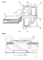
- Figure 1 shows the known structure of an inventive Printed circuit board 10, which serves to dissipate heat Has heat sink 2, which with an insulation layer 1 one possibly for the later formation of conductor tracks serving metal layer 3 is connected.
- metal layer 3 which is preferably made of copper
- Heatsink 2 covered and thus, e.g. when immersed in a Etching bath protected against corrosion.
- a sealing material 4 enclosed so that the heat sink 2 is completely covered is. This prevents through during the etching process parts detached from the heat sink 2 contaminate the etching bath.
- Figure 2 shows the circuit board 10 after processing or Structuring of the metal layer 3 and subsequent Removal of the sealing material 4.
- the laminate shown in Figure 1 is therefore the base material particularly well suited for the production of printed circuit boards.
- the preferably plate-shaped heat sink 2 made of aluminum give the circuit board 10 a high stability, so that thin insulation layers 1 can be used.
- the fat the insulation layer 1 is preferably in the range from 1% - 10% of the thickness of the heat sink plate 2, the for example, is only a few millimeters.
- the printed circuit board 10 shown in FIG. 1 is manufactured by on one side of an insulation layer 1 preferably plate-shaped heat sink 2 made of aluminum and on the other hand one for the later formation of Conductor serving metal layer 3 made of copper becomes.
- the layers 1, 2 and 3 mentioned are by means of a supplied adhesive or by means of as an adhesive serving insulation layer 1 connected together.
- the Layers 1, 2 and 3 are preferably connected simultaneously with the connection of the sealing material 4 Pressure, possibly with simultaneous supply of heat.
- the insulation layer 1 is made preferably made of a resin, e.g. epoxy resin, impregnated glass fiber braid, which is called PREPREG is known (see e.g. [1], page 53). Because the resin at this material is only partially polymerized this under pressure, possibly under Heat supply, liquefied, so that the generated Liquid penetrates into the adjacent layers and itself connects with them or at least adheres to them.
- a resin e.g. epoxy resin, impregnated glass fiber braid, which is called PREPREG is known (see e.g. [1], page 53).
- the sealing material 4 is preferably also made of one with synthetic resin, e.g. Epoxy resin, impregnated glass fiber braid, like FR4, which compared to PREPREG one has increased degree of polymerization.
- synthetic resin e.g. Epoxy resin, impregnated glass fiber braid, like FR4
- the insulation layer 1 and the sealing material 4 are in the dimensions preferably chosen such that they are overlap each other and therefore connect with each other as soon as the insulation layer 1 is liquefied under pressure.
- index and Manufacturing holes are provided which the Facilitate implementation of subsequent manufacturing processes.
- FIG. 3 shows the known structure of a production benefit 100 with oppositely directed heat sinks 2a, 2b, the enclosed on the edge by sealing material 4 and on the sides facing away from one another via insulation layers 1a, 1b are connected to metal layers 3a, 3b so that they connecting the individual layers completely covered are.
- the insulation layers 1a, 1b and the metal layers 3a, 3b overlap the sealing material surrounding the heat sink 2a, 2b 4 such that after pressing the layers a good connection between the insulation layers 1a, 1b and the metal layers 3a, 3b and the sealing material 4 arises.
- the two-layer production benefit 100 is used, for example, to produce two printed circuit boards 10a, 10b or n-by-two printed circuit boards 10a 1 , ..., 10a n or 10b 1 , ..., 10b n
- the two layers of the production benefit 100 which serve to form printed circuit boards 10a 1 , ..., 10a n and 10b 1 , ..., 10b n are thus held together by the sealing material 4 adhering to the insulation layers 1a, 1b on both sides.
- the laminate 100 or the printed circuit boards 10a 1 , ..., 10a n or 10b 1 , ..., 10b n are normally conveyed and processed by means of rapidly clocked machines
- the laminate layers 1a; 1b, 2a; 2b, 3a; 3b are usually subjected to strong temperature changes, as a result of which bulges can occur which can impede further processing, for example the precise detection, processing and conveying of the production benefit 100.
- the layer is made up of two layers existing manufacturing benefits 100 therefore under a vacuum pressed and tightly glued that get a vacuum in it remains, which stabilizes the manufacturing benefit 100 and prevents, for example, by temperature expansion causes bulges in the laminate layers 1a; 1b, 2a; 2 B, 3a; 3b can arise.
- the laminate layers 1a; 1b, 2a; 2 B, 3a; 3b are therefore due to the external atmospheric pressure pressed together and kept stable. Thermal strains that in the laminate layers 1a; 1b, 2a; 2b, 3a; 3b, in particular in the heat sinks 2a; 2b can occur, compensate each other also thanks to the symmetrical structure of the manufacturing benefits 100th
- the just aligned manufacturing benefit 100 can be in the others, usually carried out by machines Process steps, for example by means of those in FIG. 11 shown manufacturing and index holes without problems capture, transport and edit precisely.
- the sealing material 4 is detached from the manufacturing benefit 100, for example by cutting, scoring, milling or punching along the dividing line 6 shown in FIG. 3, after which the printed circuit boards 10a 1 , ..., 10a n or 10b 1 , ... , 10b n can be separated while removing the vacuum.
- FIG 4 shows a large, two-layer Base material benefit 200, in which four production benefits 1001, ..., 1004 are summarized, of which the one shown in FIG Manufacturing benefit 100 by milling or punching along the Separation line 60 are separated and processed can.
- the hatching material 4 is shown hatched, which, as shown in Figure 3, the heat sink 2 tight encloses.
- Both sides of the sealing material 4 and the the heat sink 2a1, ..., 2a8 or 2b1, ..., 2b8 are each with an insulation layer 1a or 1b and a metal layer 3a or 3b lying thereon.
- the laminate of the thus formed Base material benefit 200 pressed under vacuum and tightly glued so that a vacuum is maintained, which the laminate stabilized.
- connections between the Heatsink 2 and parts 34 preferably already structured metal layer 3 are created, which one minimal electrical as well as minimal thermal Have resistance and thus to solve problems regarding the shielding of electromagnetic waves and the selective derivation of heat energy required are suitable.
- connection 8 is produced according to the invention, by material 202 of the heat sink 2 in the area of a Cooling connection or ground connection 34 of the structured Metal layer 3 through the insulation layer 1 and Metal layer 2 pressed through and by pressure in Is pressed against the metal layer 3 in such a way that it partially overlaps and contacts the metal layer 3, which makes excellent electrical and thermal Connection 8 between the heat sink 2 and the cooling connection or ground connection 34 is created.
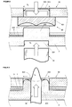
- FIG. 5 shows such a connection 8 in the material 202 of the heat sink 2 through the insulation layer 1 and the Metal layer 3 shifted through and then was pressed against it, so that an outside on the Metal layer 3 adjacent flange or rivet head 2020 was formed.
- Heatsink 2 has a stamp on its underside caused indentation 201, the volume of which the moved material 202 corresponds.
- one is preferably used uses at least one die 92 provided with an opening 920, which, as shown in Figure 6, in such a way to the one to be machined PCB is created that the opening 920 at the Point where the metal layer 3 rests, where the connection 8 should arise. Then one becomes at least approximately Stamp 91 aligned coaxially to the die opening 920 pressed against the heat sink 2, thereby overlying Material 202 of the heat sink 2 into the die opening 920 is pushed into it.
- the diameter d S of the punch 91 for example provided with a circular cross section, by means of which the material is to be displaced, is preferably chosen to be a few hundredths of a millimeter smaller than the diameter d M of the die opening 920, which is adapted to the shape of the punch 91. This results in a reduced load on the tools, the punch 91 and the die 92, and thus a reduction in the maintenance effort.
- displaced material 202 is preferably used in another Method step, as shown in FIG. 8, a tool 93 in the die opening 920 inserted, by means of which the displaced material 202 against the example by means of the stamp 91 or by means of a pressure plate held circuit board is pressed that the material 202 too a flange contacting the metal layer 3 or Rivet head 2020 is pressed (see Figure 7).
- the tool 93 has a piston 930 that can be inserted into the die opening 920 and an associated, open against the metal layer 3 Plate 931 on, with one for distributing the material 202nd serving profile 93 is provided.
- 91 is also used instead of a stamp a candle-shaped mandrel 94 can be used, for example at least approximately coaxially to the die opening 920 aligned through the heat sink 2 into the die opening 920 is introduced, whereby punctured material 202 of the Heatsink 2 displaced into the die opening 920 becomes.
- the die 92 if necessary piercing mandrel 94 is at corresponding design of the die opening 920 also possible that the material 202 in only one step in displaced the die opening 920 and further against the Metal layer 3 is pressed.
- This channel 203 the corresponds to the outer dimensions of the mandrel 94 if necessary, can be used to run a cable, by means of its electrical components, if necessary Sensors that can be connected.
- connections 8 on one or more in a manufacturing benefit of printed circuit boards 10 can be manufactured at the same time.
- connection 8 produced in this way can be used as a thermal and / or as an electrical bridge between the heat sink 2 and serve the metal layer 3.
- a big one Ground connection provided, which also serves as a cooling connection serves on which the housing of an integrated to be cooled Circuit is placed that is above average Amount of heat energy generated.
- any materials for the layer structure the laminates selectable.
- the metal layer 3 is preferably with Placed gold.
- other layers are in the laminate insertable.
- the ground connections of course, can also be created before the circuit boards are punched out become.
- figure 10 shows the manufacturing benefit 100 after processing the first Metal layer 3a, 3b and the application and processing of two further insulation and metal layers 1a ', 1a "; 1b', 1b “or 3a ', 3a' '; 3b', 3b '' and with the connection of the Metal layers 3, 3a ', 3a' '; 3, 3b ', 3b "serving, so-called microvias 20, 21, 22.
- This also has two layers multilayer manufacturing benefit 100 is preferably below Vacuum pressed and provided with connections 8 if necessary, which is the outermost metal layer 3 "or one therein provided cooling connection or ground connection with the Connect heat sink 2.
- FIG. 11 shows the production benefit 100 from FIG. 3 provided with index and manufacturing bores 1001,... 1005 with, for example, drawn-in dividing lines 6, which indicate that the production benefit 100 in each of the two layers has up to fourteen or more printed circuit boards 10a 1 ,. .., 10a 14 or 10b 1 , ..., 10b 14 may include.
- Figure 12 shows a die 930 with an integrated therein Tool 93, by means of which the displaced material 202 is closed a flange or rivet head is pressed.
- the creation of the Compound according to the invention can therefore by the person skilled in the art with different tools in appropriately adapted Procedural steps take place.
Landscapes
- Engineering & Computer Science (AREA)
- Microelectronics & Electronic Packaging (AREA)
- Manufacturing & Machinery (AREA)
- Structure Of Printed Boards (AREA)
- Insulated Metal Substrates For Printed Circuits (AREA)
- Production Of Multi-Layered Print Wiring Board (AREA)
Abstract
Description
- Figur 1
- den bekannten Aufbau einer erfindungsgemässen Leiterplatte 10 mit einem Kühlkörper 2, der über eine Isolationsschicht 1 mit einer Metallschicht 3 verbunden ist und der mittels eines Dichtungsmaterials 4 dicht abgeschlossen ist,
- Figur 2
- die Leiterplatte 10 von Figur 1, nach der Bearbeitung der Metallschicht 3 und der Entfernung des Dichtungsmaterials 4, versehen mit einer schematisch dargestellten elektrischen Verbindung 8 zwischen dem Kühlkörper und der Metallschicht,
- Figur 3
- den bekannten Aufbau eines zweilagigen zur Herstellung von zwei oder n-mal-zwei Leiterplatten dienenden Fabrikationsnutzens 100 mit gegeneinander gerichteten Kühlkörpern 2a; 2b, die von Dichtungsmaterial 4 umschlossen sind,
- Figur 4
- eine Seite eines Basismaterialnutzens 200, der vier Fabrikationsnutzen 1001, ..., 1004 mit in Ausnehmungen 41, ..., 44 eines Dichtungsmaterials 4 eingeschlossenen Kühlkörpern 2a1, ..., 2a4; 2b1, ..., 2b8 aufweist,
- Figur 5
- eine erfindungsgemäss gefertigte Verbindung 8 einer Leiterplatte 10 gemäss Figur 2,
- Figur 6
- eine mit einer Öffnung 920 versehene Matrize 92 und ein Stempel 91, die zur Fertigung der Verbindung 8 an die Leiterplatte 10 angelegt werden,
- Figur 7
- die Matrize 92 und den Stempel 91 nach Durchführung eines ersten Verfahrensschritts, durch den Material 202 des Kühlkörpers 2 in die Öffnung 920 hinein verschoben wurde,
- Figur 8
- die Matrize 92 mit einem in die Öffnung 920 eingesetzten Werkzeug 93, mittels dessen das verschobene Material 202 zu einem Flansch oder Nietkopf verpresst wird,
- Figur 9
- die Verschiebung des Materials 202 in die Öffnung 920 der Matrize 92 mittels eines kerzenförmigen Dorns 94,
- Figur 10
- den Fertigungsnutzen 100 nach Bearbeitung der ersten Metallschicht 3a, 3b und dem Auftrag und der Bearbeitung von zwei weiteren Isolations- und Metallschichten 1a', 1a"; 16', 1b" bzw. 3a', 3a''; 3b', 3b' ' sowie mit der Verbindung der Metallschichten 3, 3a', 3a''; 3, 3b', 3b'' dienenden Microvias 20, 21, 22,
- Figur 11
- den Fertigungsnutzen 100 von Figur 3 mit der Fabrikation dienenden Index- und Fabrikationsbohrungen 1001, ..., 1005, die in neutrale Zonen des später abzutrennenden Randbereichs des Laminats 100 eingefügt sind, und
- Figur 12
- eine Matrize 930 mit einem darin integrierten Werkzeug 93, mittels dessen das verschobene Material 202 zu einem Flansch oder Nietkopf verpresst wird.
- [1]
- G. Herrmann, K. Egerer, Handbuch der Leiterplattentechnik, Band 2, Eugen G. Leuze Verlag, Saulgau 1991
- [2]
- U.S. Patent 5,953,208
- [3]
- EP 0 902 609 A1
- [4]
- CH-Patent 691 277
- [5]
- Marco Leone, On the Coupling of an External Electromagnetic Field to a Printed Circuit Board Trace, IEEE Transactions on EMC, November 1999, pages 418-424
Claims (14)
- Verfahren zur Bearbeitung einer Leiterplatte (10), die einen metallenen Kühlkörper (2) aufweist, der mittels einer Isolationsschicht (1) mit einer strukturierten Metallschicht (3) verbunden ist, dadurch gekennzeichnet, dass Material (202) des Kühlkörpers (2) im Bereich eines Kühlanschlusses und/oder eines Masseanschlusses (34) durch die Isolationsschicht (1) und die Metallschicht (3) hindurch gedrückt und mittels Druck in Richtung zur Metallschicht (3) derart gegengepresst wird, dass es die Metallschicht (3) überlappt und kontaktiert, wodurch eine thermische und elektrische Verbindung (8) zwischen dem Kühlkörper (2) und dem Kühlanschlusses bzw. dem Masseanschluss (34) geschaffen wird.
- Verfahren nach Anspruch 1, dadurch gekennzeichnet, dass eine mit wenigstens einer Öffnung (920) versehene Matrize (92) vorgesehen ist, die derart an die zu bearbeitende Leiterplatte (10) angelegt wird, dass die Öffnung (920) an der Stelle, an der Metallschicht (3) anliegt, an der die Verbindung (8) entstehen soll, wonach ein zumindest annähernd koaxial zur Öffnung (920) ausgerichteter Stempel (91) gegen den Kühlkörper (2) gepresst wird, wodurch darüber liegendes Material (202) des Kühlkörpers (2) in die Öffnung (920) hinein verdrängt wird.
- Verfahren nach Anspruch 2, dadurch gekennzeichnet, dass der Durchmesser des vorzugsweise runden Stempels (91) einige Hundertstel eines Millimeters kleiner ist als der Durchmesser der vorzugsweise runden Öffnung.
- Verfahren nach Anspruch 1, dadurch gekennzeichnet, dass eine mit wenigstens einer Öffnung (920) versehene Matrize (92) vorgesehen ist, die derart an die bearbeitende Leiterplatte (10) angelegt wird, dass die Öffnung (920) an der Stelle, an der Metallschicht (3) anliegt, an der die Verbindung (8) entstehen soll, wonach ein zumindest annähernd koaxial zur Öffnung (920) ausgerichteter vorzugsweise kerzenförmiger Dorn (94) durch den Kühlkörper (2) in die Öffnung (920) hineingeführt wird, wodurch durchstossenes Material (202) des Kühlkörpers (2) in die Öffnung (920) hinein verdrängt wird.
- Verfahren nach Anspruch 2 oder 4, dadurch gekennzeichnet, dass ein Werkzeug (93) in die Öffnung (920) der angehobenen Matrize (92) oder daneben auf gleicher Ebene, eingesetzt wird, oder dass eine weitere Matrize (930) mit mit wenigstens einem darin integrierten Werkzeugen (93) vorgesehen ist, mittels dessen das verdrängte Material (202) derart gegen die fest gehaltene Leiterplatte (10) gedrückt wird, dass es zu einem die Metallschicht (3) kontaktierenden Flansch oder Nietkopf , (2020) gepresst wird.
- Verfahren nach einem der Ansprüche 1 bis 5, dadurch gekennzeichnet, dass mehrere Verbindungen (8) auf einer oder mehreren in einem Fertigungsnutzen (200) enthaltener Leiterplatten (10; 10a1, ..., 10a8) gleichzeitig gefertigt werden.
- Verfahren zur Herstellung von wenigstens zwei je mit einem Kühlkörper (2a, 2b) versehenen Leiterplatten (10a1, ..., 10an bzw. 10b1, ..., 10bn), bei demder resultierende aus zwei mehrschichtigen Lagen bestehende Basismaterialnutzen (200) oder Fertigungsnutzen (100) unter Vakuum derart verpresst und dicht verklebt wird, dass darin ein Vakuum erhalten bleibt.a) wenigstens zwei als Kühlkörper (2a, 2b) dienende Metallplatten aufeinander gelegt,b) randseitig von einem Dichtungsmaterial (4) umschlossen undc) an deren freiliegenden Seiten mittels einer das Dichtungsmaterial (4) überlappenden Isolationsschicht (1a; 1b) sowie, aussen daran anliegend, einer der späteren Bildung von Leiterbahnen dienenden Metallschicht (3a; 3b) abgedeckt werden, dadurch gekennzeichnet, dass
- Verfahren nach Anspruch 7, dadurch gekennzeichnet, dass der Basismaterialnutzen (200) oder der Fertigungsnutzen (100) mittels eines Klebers oder mittels der unter Druck verklebenden Isolationsschichten (1a, 1b) verpresst und verklebt wird.
- Verfahren nach Anspruch 7 oder 8, dadurch gekennzeichnet, dass die Isolationsschichten (1a, 1b) aus einem nur teilweise auspolymerisierten glasfaserverstärkten Polymerwerkstoff wie PREPREG bestehen, der sich unter Druck, gegebenenfalls zusätzlich unter Wärmezufuhr, zumindest teilweise verflüssigt und als Klebstoff dient.
- Verfahren nach Anspruch 7, 8 oder 9, dadurch gekennzeichnet, dass in den Zonen, in denen die Isolationsschichten (1a, 1b) und die Metallschichten (3a, 3b) das Dichtungsmaterial (4) überlappen, Index- und/oder Fasbrikationsbohrungen vorgesehen werden.
- Verfahren nach einem der Ansprüche 7 bis 10, dadurch gekennzeichnet, dass wenigstens die Zonen, in denen die Isolationsschichten (1a, 1b) und die Metallschichten (3a, 3b) das Dichtungsmaterial (4) überlappen, gegebenenfalls mit einem zusätzlichen Anteil der Kühlkörper (2a, 2b), vom bearbeiteten Ferigungsnutzen (100) abgetrennt werden, wodurch die Leiterplatten (10a1, ..., 10an bzw. 10b1, ..., 10bn) vereinzelt werden können.
- Verfahren nach einem der Ansprüche 7 bis 11, dadurch gekennzeichnet, dass der Fertigungsnutzen (100) mit weiteren Isolations- und Metallschichten (1a' , 1a"; 1b' , 1b" bzw. 3a' , 3a"; 3b' , 3b") sowie mit der Verbindung der Metallschichten (3, 3a' , 3a" ; 3, 3b' , 3b'') dienenden Microvias (20, 21, 22) versehen wird.
- Leiterplatte (10) mit einem metallenen Kühlkörper (2), der mittels einer Isolationsschicht (1) und gegebenenfalls weiteren Laminatschichten mit einer strukturierten Metallschicht (3) verbunden ist, welche für eine elektronische Schaltung vorgesehenen Leiterbahnen (31, 32, 33) und wenigstens einen mit einem Halbleiter verbundenen oder verbindbaren Kühlanschluss oder einen Masseanschluss (34) bildet, dadurch gekennzeichnet, dass Material (202) des Kühlkörpers (2) im Bereich des Kühlanschlusses oder des Masseanschlusses (34) durch die Isolationsschicht (1) und die Metallschicht (3) hindurch geführt und mit dieser verbunden ist.
- Leiterplatte (10) nach Anspruch 12, dadurch gekennzeichnet, dass das vom Kühlkörper (2) durch die Metallschicht (3) geführte Material (202), das gegebenenfalls einen die Laminatschichten (1, 2, 3) durchstossenden Kanal umschliesst, einen Flansch oder Nietkopf (2020) bildet, der an der Metallschicht (3) anliegt und diese kontaktiert.
Priority Applications (2)
| Application Number | Priority Date | Filing Date | Title |
|---|---|---|---|
| AT02405740T ATE513454T1 (de) | 2002-08-29 | 2002-08-29 | Verfahren zur bearbeitung und herstellung von leiterplatten sowie leiterplatte |
| EP02405740A EP1395100B1 (de) | 2002-08-29 | 2002-08-29 | Verfahren zur Bearbeitung und Herstellung von Leiterplatten sowie Leiterplatte |
Applications Claiming Priority (1)
| Application Number | Priority Date | Filing Date | Title |
|---|---|---|---|
| EP02405740A EP1395100B1 (de) | 2002-08-29 | 2002-08-29 | Verfahren zur Bearbeitung und Herstellung von Leiterplatten sowie Leiterplatte |
Publications (2)
| Publication Number | Publication Date |
|---|---|
| EP1395100A1 true EP1395100A1 (de) | 2004-03-03 |
| EP1395100B1 EP1395100B1 (de) | 2011-06-15 |
Family
ID=31198012
Family Applications (1)
| Application Number | Title | Priority Date | Filing Date |
|---|---|---|---|
| EP02405740A Expired - Lifetime EP1395100B1 (de) | 2002-08-29 | 2002-08-29 | Verfahren zur Bearbeitung und Herstellung von Leiterplatten sowie Leiterplatte |
Country Status (2)
| Country | Link |
|---|---|
| EP (1) | EP1395100B1 (de) |
| AT (1) | ATE513454T1 (de) |
Cited By (2)
| Publication number | Priority date | Publication date | Assignee | Title |
|---|---|---|---|---|
| WO2019110549A1 (de) * | 2017-12-08 | 2019-06-13 | HELLA GmbH & Co. KGaA | Verfahren zur herstellung eines leiterplatten-kühlkörper-aufbaus und aufbau aus leiterplatte und kühlkörper hierzu |
| DE102018101264A1 (de) | 2018-01-22 | 2019-07-25 | HELLA GmbH & Co. KGaA | Leiterplatten- Kühlkörper- Aufbau und Verfahren hierzu |
Citations (9)
| Publication number | Priority date | Publication date | Assignee | Title |
|---|---|---|---|---|
| US3882264A (en) * | 1967-12-29 | 1975-05-06 | Amp Inc | Eyelet in flexible circuitry |
| JPS63114197A (ja) * | 1986-10-31 | 1988-05-19 | 三菱電機株式会社 | 金属ベ−スプリント配線板の製造方法 |
| US5220487A (en) * | 1992-01-27 | 1993-06-15 | International Business Machines Corporation | Electronic package with enhanced heat sinking |
| EP0561620A2 (de) * | 1992-03-19 | 1993-09-22 | Hitachi, Ltd. | Leiterschicht-Anordnungen und das Herstellen ihrer elektrischen Verbindungen |
| JPH0851267A (ja) * | 1994-08-08 | 1996-02-20 | Sankyo Seiki Mfg Co Ltd | 回路基板及びその製造方法 |
| JPH08228056A (ja) * | 1995-02-21 | 1996-09-03 | Denki Kagaku Kogyo Kk | 金属ベース回路基板 |
| DE19650813A1 (de) * | 1996-12-07 | 1998-06-10 | Univ Dresden Tech | Folienleiterplattensystem |
| EP1063873A2 (de) * | 1999-06-22 | 2000-12-27 | Dr.-Ing. Jürgen Schulz-Harder | Verfahren zum Herstellen von Substraten mit strukturierten Metallisierungen sowie Halte-und Fixierelement zur Verwendung bei dem Verfahren |
| CH691277A5 (de) * | 2000-02-29 | 2001-06-15 | Ascom Ag | Verfahren zur Herstellung von Leiterplatten sowie Leiterplatte. |
Family Cites Families (1)
| Publication number | Priority date | Publication date | Assignee | Title |
|---|---|---|---|---|
| DE10045359A1 (de) * | 2000-09-14 | 2002-03-28 | Gerald Hecht | Vorrichtung zum Aufbringen von Lotpaste auf eine Leiterplatte |
-
2002
- 2002-08-29 EP EP02405740A patent/EP1395100B1/de not_active Expired - Lifetime
- 2002-08-29 AT AT02405740T patent/ATE513454T1/de active
Patent Citations (9)
| Publication number | Priority date | Publication date | Assignee | Title |
|---|---|---|---|---|
| US3882264A (en) * | 1967-12-29 | 1975-05-06 | Amp Inc | Eyelet in flexible circuitry |
| JPS63114197A (ja) * | 1986-10-31 | 1988-05-19 | 三菱電機株式会社 | 金属ベ−スプリント配線板の製造方法 |
| US5220487A (en) * | 1992-01-27 | 1993-06-15 | International Business Machines Corporation | Electronic package with enhanced heat sinking |
| EP0561620A2 (de) * | 1992-03-19 | 1993-09-22 | Hitachi, Ltd. | Leiterschicht-Anordnungen und das Herstellen ihrer elektrischen Verbindungen |
| JPH0851267A (ja) * | 1994-08-08 | 1996-02-20 | Sankyo Seiki Mfg Co Ltd | 回路基板及びその製造方法 |
| JPH08228056A (ja) * | 1995-02-21 | 1996-09-03 | Denki Kagaku Kogyo Kk | 金属ベース回路基板 |
| DE19650813A1 (de) * | 1996-12-07 | 1998-06-10 | Univ Dresden Tech | Folienleiterplattensystem |
| EP1063873A2 (de) * | 1999-06-22 | 2000-12-27 | Dr.-Ing. Jürgen Schulz-Harder | Verfahren zum Herstellen von Substraten mit strukturierten Metallisierungen sowie Halte-und Fixierelement zur Verwendung bei dem Verfahren |
| CH691277A5 (de) * | 2000-02-29 | 2001-06-15 | Ascom Ag | Verfahren zur Herstellung von Leiterplatten sowie Leiterplatte. |
Non-Patent Citations (5)
| Title |
|---|
| "HEAT TRANSFER IMPROVEMENT FOR THERMAL CARRIER CIRCUIT CARDS", IBM TECHNICAL DISCLOSURE BULLETIN, IBM CORP. NEW YORK, US, vol. 35, no. 2, 1 July 1992 (1992-07-01), pages 498 - 499, XP000313373, ISSN: 0018-8689 * |
| 31447: "ELECTRICAL CONNECTION BY DISPLACEMENT OF INTERNAL PLATES", RESEARCH DISCLOSURE, KENNETH MASON PUBLICATIONS, HAMPSHIRE, GB, no. 314, 1 June 1990 (1990-06-01), pages 492, XP000132344, ISSN: 0374-4353 * |
| DATABASE WPI Week 198826, Derwent World Patents Index; AN 1988-178097, XP002138912 * |
| PATENT ABSTRACTS OF JAPAN vol. 1996, no. 06 28 June 1996 (1996-06-28) * |
| PATENT ABSTRACTS OF JAPAN vol. 1997, no. 01 31 January 1997 (1997-01-31) * |
Cited By (7)
| Publication number | Priority date | Publication date | Assignee | Title |
|---|---|---|---|---|
| WO2019110549A1 (de) * | 2017-12-08 | 2019-06-13 | HELLA GmbH & Co. KGaA | Verfahren zur herstellung eines leiterplatten-kühlkörper-aufbaus und aufbau aus leiterplatte und kühlkörper hierzu |
| CN111466159A (zh) * | 2017-12-08 | 2020-07-28 | 海拉有限双合股份公司 | 用于制造电路板-散热体结构的方法以及对此的包括电路板和散热体的结构 |
| US11240905B2 (en) | 2017-12-08 | 2022-02-01 | HELLA GmbH & Co. KGaA | Method for producing a printed circuit board-cooling body structure |
| CN111466159B (zh) * | 2017-12-08 | 2023-07-25 | 海拉有限双合股份公司 | 用于制造电路板-散热体结构的方法以及对此的包括电路板和散热体的结构 |
| DE102018101264A1 (de) | 2018-01-22 | 2019-07-25 | HELLA GmbH & Co. KGaA | Leiterplatten- Kühlkörper- Aufbau und Verfahren hierzu |
| WO2019141594A1 (de) | 2018-01-22 | 2019-07-25 | HELLA GmbH & Co. KGaA | Leiterplatten- kühlkörper- aufbau und verfahren hierzu |
| US11523498B2 (en) | 2018-01-22 | 2022-12-06 | HELLA GmbH & Co. KGaA | Circuit board heat sink structure and method therefor |
Also Published As
| Publication number | Publication date |
|---|---|
| ATE513454T1 (de) | 2011-07-15 |
| EP1395100B1 (de) | 2011-06-15 |
Similar Documents
| Publication | Publication Date | Title |
|---|---|---|
| EP2260683B1 (de) | Verfahren zur herstellung einer elektronischen baugruppe | |
| AT503718B1 (de) | Herstellung einer eine komponente umfassenden schicht | |
| DE2946726C2 (de) | Leiterplatte mit starren und flexiblen Bereichen und Verfahren zu deren Herstellung | |
| DE4422216A1 (de) | Mehrlagige metallische Leiterplatte und gegossener Baustein | |
| DE2541282A1 (de) | Verfahren zur herstellung von durchgangsloechern in einem laminat | |
| DE1065903B (de) | Verfahren und Vorrichtung zur Herstellung von leitenden Mustern | |
| WO2015077808A1 (de) | Leiterplattenstruktur | |
| DE102016222631A1 (de) | Leiterplattenanordnung mit einem elektrischen Bauteil und einem Kühlkörper | |
| DE102018203715B4 (de) | Verfahren zur Herstellung einer Leiterplatte unter Verwendung einer Form für Leiterelemente | |
| EP0620702A2 (de) | Kern für elektrische Verbindungssubstrate und elektrische Verbindungssubstrate mit Kern, sowie Verfahren zu deren Herstellung | |
| EP0917417A2 (de) | Verfahren zur Erzeugung einer Montageplatte | |
| CH667359A5 (de) | Verfahren zur herstellung einer starre und flexible partien aufweisenden leiterplatte fuer gedruckte elektrische schaltungen. | |
| EP0406678A1 (de) | Quellmittel zur Vorbehandlung von Kunstharzen vor einer stromlosen Metallisierung | |
| DE69005961T2 (de) | Verfahren zur Herstellung einer defektfreien Oberfläche auf einem porösen keramischen Substrat. | |
| EP0126856A2 (de) | Verfahren zum Herstellen von Leiterplatten mit starren und flexiblen Bereichen | |
| EP0897654A1 (de) | Verfahren zur herstellung elektrisch leitender verbindungen zwischen zwei oder mehr leiterstrukturen | |
| EP1395100B1 (de) | Verfahren zur Bearbeitung und Herstellung von Leiterplatten sowie Leiterplatte | |
| DE3302857A1 (de) | Verfahren zum herstellen von vorlaminaten fuer starrflexible leiterplatten | |
| DE3624718A1 (de) | Mehrlagige, starre und flexible bereiche aufweisende leiterplatte | |
| EP0394678A2 (de) | Mehrlagen-Leiterplatten für Feinleiter und Verfahren zu ihrer Herstellung | |
| DE60130108T2 (de) | Verfahren zur herstellung elektrischer verbindungselemente und verbindungselement | |
| DE102018125008B4 (de) | Verfahren zur Kontaktierung von in einer Platine eingebetteten metallischen Einlegestücken sowie Platine mit metallischen Einlegestücken | |
| DE102018100139A1 (de) | Verfahren zum Herstellen einer mehrlagigen Leiterplatte sowie Leiterplatte | |
| DE3423181A1 (de) | Verfahren zur herstellung von vorlaminaten fuer mehrlagenleiterplatten | |
| DE3935680A1 (de) | Verfahren zum herstellen einer metallkern-leiterplatte |
Legal Events
| Date | Code | Title | Description |
|---|---|---|---|
| PUAI | Public reference made under article 153(3) epc to a published international application that has entered the european phase |
Free format text: ORIGINAL CODE: 0009012 |
|
| AK | Designated contracting states |
Kind code of ref document: A1 Designated state(s): AT BE BG CH CY CZ DE DK EE ES FI FR GB GR IE IT LI LU MC NL PT SE SK TR |
|
| AX | Request for extension of the european patent |
Extension state: AL LT LV MK RO SI |
|
| 17P | Request for examination filed |
Effective date: 20040903 |
|
| AKX | Designation fees paid |
Designated state(s): AT BE BG CH CY CZ DE DK EE ES FI FR GB GR IE IT LI LU MC NL PT SE SK TR |
|
| RAP1 | Party data changed (applicant data changed or rights of an application transferred) |
Owner name: ASETRONICS AG |
|
| 17Q | First examination report despatched |
Effective date: 20081029 |
|
| GRAP | Despatch of communication of intention to grant a patent |
Free format text: ORIGINAL CODE: EPIDOSNIGR1 |
|
| GRAS | Grant fee paid |
Free format text: ORIGINAL CODE: EPIDOSNIGR3 |
|
| GRAA | (expected) grant |
Free format text: ORIGINAL CODE: 0009210 |
|
| AK | Designated contracting states |
Kind code of ref document: B1 Designated state(s): AT BE BG CH CY CZ DE DK EE ES FI FR GB GR IE IT LI LU MC NL PT SE SK TR |
|
| REG | Reference to a national code |
Ref country code: GB Ref legal event code: FG4D Free format text: NOT ENGLISH Ref country code: CH Ref legal event code: EP |
|
| REG | Reference to a national code |
Ref country code: IE Ref legal event code: FG4D Free format text: LANGUAGE OF EP DOCUMENT: GERMAN |
|
| REG | Reference to a national code |
Ref country code: DE Ref legal event code: R096 Ref document number: 50215088 Country of ref document: DE Effective date: 20110721 |
|
| REG | Reference to a national code |
Ref country code: CH Ref legal event code: NV Representative=s name: PETER RUTZ |
|
| REG | Reference to a national code |
Ref country code: NL Ref legal event code: VDEP Effective date: 20110615 |
|
| PG25 | Lapsed in a contracting state [announced via postgrant information from national office to epo] |
Ref country code: SE Free format text: LAPSE BECAUSE OF FAILURE TO SUBMIT A TRANSLATION OF THE DESCRIPTION OR TO PAY THE FEE WITHIN THE PRESCRIBED TIME-LIMIT Effective date: 20110615 |
|
| PG25 | Lapsed in a contracting state [announced via postgrant information from national office to epo] |
Ref country code: FI Free format text: LAPSE BECAUSE OF FAILURE TO SUBMIT A TRANSLATION OF THE DESCRIPTION OR TO PAY THE FEE WITHIN THE PRESCRIBED TIME-LIMIT Effective date: 20110615 Ref country code: CY Free format text: LAPSE BECAUSE OF FAILURE TO SUBMIT A TRANSLATION OF THE DESCRIPTION OR TO PAY THE FEE WITHIN THE PRESCRIBED TIME-LIMIT Effective date: 20110615 Ref country code: GR Free format text: LAPSE BECAUSE OF FAILURE TO SUBMIT A TRANSLATION OF THE DESCRIPTION OR TO PAY THE FEE WITHIN THE PRESCRIBED TIME-LIMIT Effective date: 20110916 |
|
| PG25 | Lapsed in a contracting state [announced via postgrant information from national office to epo] |
Ref country code: NL Free format text: LAPSE BECAUSE OF FAILURE TO SUBMIT A TRANSLATION OF THE DESCRIPTION OR TO PAY THE FEE WITHIN THE PRESCRIBED TIME-LIMIT Effective date: 20110615 |
|
| REG | Reference to a national code |
Ref country code: IE Ref legal event code: FD4D |
|
| PG25 | Lapsed in a contracting state [announced via postgrant information from national office to epo] |
Ref country code: CZ Free format text: LAPSE BECAUSE OF FAILURE TO SUBMIT A TRANSLATION OF THE DESCRIPTION OR TO PAY THE FEE WITHIN THE PRESCRIBED TIME-LIMIT Effective date: 20110615 Ref country code: IE Free format text: LAPSE BECAUSE OF FAILURE TO SUBMIT A TRANSLATION OF THE DESCRIPTION OR TO PAY THE FEE WITHIN THE PRESCRIBED TIME-LIMIT Effective date: 20110615 Ref country code: PT Free format text: LAPSE BECAUSE OF FAILURE TO SUBMIT A TRANSLATION OF THE DESCRIPTION OR TO PAY THE FEE WITHIN THE PRESCRIBED TIME-LIMIT Effective date: 20111017 Ref country code: EE Free format text: LAPSE BECAUSE OF FAILURE TO SUBMIT A TRANSLATION OF THE DESCRIPTION OR TO PAY THE FEE WITHIN THE PRESCRIBED TIME-LIMIT Effective date: 20110615 |
|
| BERE | Be: lapsed |
Owner name: ASETRONICS A.G. Effective date: 20110831 |
|
| PG25 | Lapsed in a contracting state [announced via postgrant information from national office to epo] |
Ref country code: SK Free format text: LAPSE BECAUSE OF FAILURE TO SUBMIT A TRANSLATION OF THE DESCRIPTION OR TO PAY THE FEE WITHIN THE PRESCRIBED TIME-LIMIT Effective date: 20110615 |
|
| PG25 | Lapsed in a contracting state [announced via postgrant information from national office to epo] |
Ref country code: MC Free format text: LAPSE BECAUSE OF NON-PAYMENT OF DUE FEES Effective date: 20110831 |
|
| PLBE | No opposition filed within time limit |
Free format text: ORIGINAL CODE: 0009261 |
|
| STAA | Information on the status of an ep patent application or granted ep patent |
Free format text: STATUS: NO OPPOSITION FILED WITHIN TIME LIMIT |
|
| 26N | No opposition filed |
Effective date: 20120316 |
|
| GBPC | Gb: european patent ceased through non-payment of renewal fee |
Effective date: 20110915 |
|
| PG25 | Lapsed in a contracting state [announced via postgrant information from national office to epo] |
Ref country code: BE Free format text: LAPSE BECAUSE OF NON-PAYMENT OF DUE FEES Effective date: 20110831 |
|
| PG25 | Lapsed in a contracting state [announced via postgrant information from national office to epo] |
Ref country code: DK Free format text: LAPSE BECAUSE OF FAILURE TO SUBMIT A TRANSLATION OF THE DESCRIPTION OR TO PAY THE FEE WITHIN THE PRESCRIBED TIME-LIMIT Effective date: 20110615 |
|
| REG | Reference to a national code |
Ref country code: DE Ref legal event code: R097 Ref document number: 50215088 Country of ref document: DE Effective date: 20120316 |
|
| PG25 | Lapsed in a contracting state [announced via postgrant information from national office to epo] |
Ref country code: GB Free format text: LAPSE BECAUSE OF NON-PAYMENT OF DUE FEES Effective date: 20110915 |
|
| PG25 | Lapsed in a contracting state [announced via postgrant information from national office to epo] |
Ref country code: ES Free format text: LAPSE BECAUSE OF FAILURE TO SUBMIT A TRANSLATION OF THE DESCRIPTION OR TO PAY THE FEE WITHIN THE PRESCRIBED TIME-LIMIT Effective date: 20110926 |
|
| PG25 | Lapsed in a contracting state [announced via postgrant information from national office to epo] |
Ref country code: LU Free format text: LAPSE BECAUSE OF NON-PAYMENT OF DUE FEES Effective date: 20110829 |
|
| PG25 | Lapsed in a contracting state [announced via postgrant information from national office to epo] |
Ref country code: BG Free format text: LAPSE BECAUSE OF FAILURE TO SUBMIT A TRANSLATION OF THE DESCRIPTION OR TO PAY THE FEE WITHIN THE PRESCRIBED TIME-LIMIT Effective date: 20110915 |
|
| PG25 | Lapsed in a contracting state [announced via postgrant information from national office to epo] |
Ref country code: TR Free format text: LAPSE BECAUSE OF FAILURE TO SUBMIT A TRANSLATION OF THE DESCRIPTION OR TO PAY THE FEE WITHIN THE PRESCRIBED TIME-LIMIT Effective date: 20110615 |
|
| PGFP | Annual fee paid to national office [announced via postgrant information from national office to epo] |
Ref country code: CH Payment date: 20130919 Year of fee payment: 12 Ref country code: AT Payment date: 20130911 Year of fee payment: 12 Ref country code: DE Payment date: 20130829 Year of fee payment: 12 |
|
| PGFP | Annual fee paid to national office [announced via postgrant information from national office to epo] |
Ref country code: FR Payment date: 20130829 Year of fee payment: 12 |
|
| PGFP | Annual fee paid to national office [announced via postgrant information from national office to epo] |
Ref country code: IT Payment date: 20130829 Year of fee payment: 12 |
|
| REG | Reference to a national code |
Ref country code: DE Ref legal event code: R119 Ref document number: 50215088 Country of ref document: DE |
|
| REG | Reference to a national code |
Ref country code: CH Ref legal event code: PL |
|
| REG | Reference to a national code |
Ref country code: AT Ref legal event code: MM01 Ref document number: 513454 Country of ref document: AT Kind code of ref document: T Effective date: 20140829 |
|
| PG25 | Lapsed in a contracting state [announced via postgrant information from national office to epo] |
Ref country code: IT Free format text: LAPSE BECAUSE OF NON-PAYMENT OF DUE FEES Effective date: 20140829 Ref country code: LI Free format text: LAPSE BECAUSE OF NON-PAYMENT OF DUE FEES Effective date: 20140831 Ref country code: CH Free format text: LAPSE BECAUSE OF NON-PAYMENT OF DUE FEES Effective date: 20140831 |
|
| PG25 | Lapsed in a contracting state [announced via postgrant information from national office to epo] |
Ref country code: AT Free format text: LAPSE BECAUSE OF NON-PAYMENT OF DUE FEES Effective date: 20140829 |
|
| REG | Reference to a national code |
Ref country code: FR Ref legal event code: ST Effective date: 20150430 |
|
| REG | Reference to a national code |
Ref country code: DE Ref legal event code: R119 Ref document number: 50215088 Country of ref document: DE Effective date: 20150303 |
|
| PG25 | Lapsed in a contracting state [announced via postgrant information from national office to epo] |
Ref country code: DE Free format text: LAPSE BECAUSE OF NON-PAYMENT OF DUE FEES Effective date: 20150303 |
|
| PG25 | Lapsed in a contracting state [announced via postgrant information from national office to epo] |
Ref country code: FR Free format text: LAPSE BECAUSE OF NON-PAYMENT OF DUE FEES Effective date: 20140901 |