EP1398880A2 - Schaltung zur Analog-Digital-Wandlung - Google Patents
Schaltung zur Analog-Digital-Wandlung Download PDFInfo
- Publication number
- EP1398880A2 EP1398880A2 EP03255510A EP03255510A EP1398880A2 EP 1398880 A2 EP1398880 A2 EP 1398880A2 EP 03255510 A EP03255510 A EP 03255510A EP 03255510 A EP03255510 A EP 03255510A EP 1398880 A2 EP1398880 A2 EP 1398880A2
- Authority
- EP
- European Patent Office
- Prior art keywords
- analog
- signal
- digital
- converter
- node
- Prior art date
- Legal status (The legal status is an assumption and is not a legal conclusion. Google has not performed a legal analysis and makes no representation as to the accuracy of the status listed.)
- Withdrawn
Links
Images


Classifications
-
- H—ELECTRICITY
- H03—ELECTRONIC CIRCUITRY
- H03M—CODING; DECODING; CODE CONVERSION IN GENERAL
- H03M1/00—Analogue/digital conversion; Digital/analogue conversion
- H03M1/12—Analogue/digital converters
- H03M1/14—Conversion in steps with each step involving the same or a different conversion means and delivering more than one bit
- H03M1/16—Conversion in steps with each step involving the same or a different conversion means and delivering more than one bit with scale factor modification, i.e. by changing the amplification between the steps
- H03M1/164—Conversion in steps with each step involving the same or a different conversion means and delivering more than one bit with scale factor modification, i.e. by changing the amplification between the steps the steps being performed sequentially in series-connected stages
- H03M1/167—Conversion in steps with each step involving the same or a different conversion means and delivering more than one bit with scale factor modification, i.e. by changing the amplification between the steps the steps being performed sequentially in series-connected stages all stages comprising simultaneous converters
-
- H—ELECTRICITY
- H03—ELECTRONIC CIRCUITRY
- H03M—CODING; DECODING; CODE CONVERSION IN GENERAL
- H03M1/00—Analogue/digital conversion; Digital/analogue conversion
- H03M1/12—Analogue/digital converters
- H03M1/14—Conversion in steps with each step involving the same or a different conversion means and delivering more than one bit
- H03M1/16—Conversion in steps with each step involving the same or a different conversion means and delivering more than one bit with scale factor modification, i.e. by changing the amplification between the steps
- H03M1/162—Conversion in steps with each step involving the same or a different conversion means and delivering more than one bit with scale factor modification, i.e. by changing the amplification between the steps the steps being performed sequentially in a single stage, i.e. recirculation type
Definitions
- the present invention relates to an analog-digital conversion circuit having a multi-stage pipeline (step flush) structure.
- step flush As the number of bits to convert has increased, however, sufficient conversion accuracy can no longer be obtained by the two-step flush method, and therefore an analog-digital conversion circuit having a multi-stage pipeline (step flush) structure has been developed. (See, for example, Japanese Patent Laid-Open No. 11-88172).
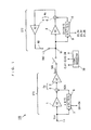
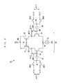
- Fig. 12 is a block diagram of a conventional analog-digital conversion circuit.
- the analog-digital conversion circuit 101 in Fig. 12 has a 10-bit, four-stage pipeline structure.
- the analog-digital conversion circuit 101 includes a sample-hold circuit 102, first to fourth stage circuits 103 to 106, a plurality of latch circuits 107, and an output circuit 108.
- the first stage circuit 103 includes a sub A/D converter 109, a D/A converter 110, an operational amplifier 111a, a subtraction circuit 112, and an operational amplifier 113.
- the subtraction circuit 112 and the operational amplifier 113 form a differential amplifier 114.
- the second and third stage circuits 104 and 105 each include a sub A/D converter 109, a D/A converter 110, an operational amplifier 111, a subtraction circuit 112 , and an operational amplifier 113.
- the subtraction circuit 112 and the operational amplifier 113 form a differential amplifier 114.
- the operational amplifier 111a in the first stage circuit 103 has a gain of 1 and serves as a sample-hold circuit.
- the operational amplifier 113 in the first stage circuit 103 and the operational amplifiers 111 and 113 in the second and third stage circuits 104 and 105 each have a gain of 2.
- the fourth (final) stage circuit 106 includes only a sub A/D converter 109.
- the first stage circuit 103 has a 4-bit structure, and the second to fourth stage circuits 104 to 106 each have a 2-bit structure.
- the number of bits (bit structure) for the sub-A/D converter 109 and the D/A converter 110 are set to be equal.
- the sample-hold circuit 102 samples an analog input signal Vin and holds the signal for a prescribed time period.
- the analog input signal Vin output from the sample-hold circuit 102 is transferred to the first stage circuit 103.
- the sub A/D converter 109 A/D-converts the analog input signal Vin.
- the result of A/D conversion by the sub A/D converter 109 a digital output of the high order 4 bits (2 9 , 2 8 , 2 7 , 2 6 ) is transferred to the D/A converter 110 and also transferred to the output circuit 108 through the four latch circuits 107.
- the D/A converter 110 converts the result of A/D conversion by the sub A/D converter 109, the 4-bit digital output into an analog signal.
- the operational amplifier 111a samples the analog input signal Vin and holds the signal for a prescribed period.
- the subtraction circuit 112 subtracts between the analog input signal Vin output from the operational amplifier 111a and the D/A conversion result by the D/A converter 110.
- the operational amplifier 113 amplifies the output of the subtraction circuit 112. The output of the operational amplifier 113 is transferred to the second stage circuit 104.
- the sub A/D converter 109 A/D-converts the output from the operational amplifier 113 in the first stage circuit 103.
- the A/D conversion result by the sub A/D converter 109 is transferred to the D/A converter 110 and also transferred to the output circuit 108 through the three latch circuits 107. In this way, a digital output of intermediate high order 2 bits (2 5 , 2 4 ) is obtained from the second stage circuit 104.
- the operational amplifier 111 amplifies the output from the operational amplifier 113 in the first stage circuit 103.
- the subtraction circuit 112 subtracts between the output of the operational amplifier 111 and the D/A conversion result by the D/A converter 110.
- the operational amplifier 113 amplifies the output of the subtraction circuit 112.
- the output of the operational amplifier 113 is transferred to the third stage circuit 105.
- the operation same as that in the second stage circuit 104 is carried out to the output from the operational amplifier 113 in the second stage circuit 104. In this way, a digital output of the intermediate low order 2 bits (2 3 , 2 2 ) is obtained from the third stage circuit 105.
- the sub A/D converter 109 A/D-converts the output from the operational amplifier 113 in the third stage circuit-105, and a digital output of the low order 2 bits (2 1 , 2 0 ) is obtained.
- the digital outputs of the first to fourth stage circuits 103 to 106 simultaneously reach the output circuit 108 through the latch circuits 107. More specifically, the latch circuits 107 are provided for synchronization among the digital outputs of the circuits 103 to 106.
- the output circuit 108 carries out digital correction to a 10-bit digital output Dout corresponding to the analog input signal Vin if necessary and then outputs the corrected output in parallel.
- the pipeline processing and amplifying function in the multiple stages allow high speed throughput (conversion frequency) and high accuracy (high resolution) to be achieved. Therefore, 8- to 12-bit structure, analog-digital conversion circuits operating with high accuracy at high speed and a conversion frequency in the range from several MHz to 100 MHz are widely used for digital video signal processing, digital communication processing and the like.
- An analog-digital conversion circuit includes a first circuit having first and second nodes, a selector that selectively applies one of an input analog signal and an analog signal at the second node to the first node, and a control device that controls the selector.
- the first circuit includes a first analog-digital converter that converts an analog signal from the first node into a digital signal, a first digital-analog converter that converts the digital signal output from the first analog-digital converter into an analog signal, and a first differential amplifier that amplifies the difference between the analog signal from the first node and the analog signal output from the first digital-analog converter and outputs the amplified difference to the second node.
- the control device controls the selector so that after the input analog signal is applied to the first node, conversion operation by the first analog-digital converter, conversion operation by the first digital-analog converter, and amplifying operation by the first differential amplifier are carried out for a prescribed number of cycles.
- analog-digital conversion circuit After the input analog signal is applied to the first node, conversion operation by the first analog-digital converter, conversion operation by the first digital-analog converter, and amplifying operation by the first differential amplifier are carried out in the first circuit for a prescribed number of cycles. In this way, a digital signal is sequentially output from the first analog-digital converter in the first circuit in each of the cycles.
- the number of cycles in the first circuit can be changed by controlling the selector, and therefore the bit resolution can readily be changed. Therefore, an analog-digital conversion circuit having variable bit resolution can readily be formed with the same hardware structure.
- the first circuit may further include a first operational amplifier that amplifies the analog signal at the first node and applies the amplified signal to the first differential amplifier.
- the first operational amplifier and the first differential amplifier in the first circuit can reduce the loop constant for the amplifiers for each stage, and the load capacitance of the amplifiers for each stage can be reduced. In this way, the limit operation frequency of each amplifier increases. Consequently, without having to improve the performance of the amplifiers, high conversion operation can be maintained while the conversion speed can be improved.
- amplifying operation by the first operational amplifier and conversion operation by the first analog-digital converter can be carried out in parallel with amplifying operation by the first differential amplifier and conversion operation by the first digital analog converter. In this way, the timing limitations for the amplifying operation by the first operational amplifier, the conversion operation by the first analog-digital converter, the conversion operation by the first digital-analog converter, and the amplifying operation by the first differential amplifier in each cycle can be relaxed.
- the analog-digital conversion circuit may further include a second circuit provided preceding the first circuit by at least one stage through the selector.
- the second circuit may include a second analog-digital converter that converts an input analog signal into a digital signal, a second digital-analog converter that converts a digital signal output from the second analog-digital converter into an analog signal, and a second differential amplifier that amplifies the difference between the input analog signal and the analog signal output from the second digital-analog converter and outputs the amplified difference to the first circuit through the selector.
- the analog signal is input to the second circuit, conversion operation by the second analog-digital converter, conversion operation by the second digital analog converter, and amplifying operation by the second differential amplifier are carried out.
- the analog signal output from the second differential amplifier is input to the first circuit through the selector, and in the first circuit, conversion operation by the first analog-digital converter, conversion operation by the first digital-analog converter, and amplifying operation by the first differential amplifier are carried out for a prescribed number of cycles.
- the digital signal is output from the second analog-digital converter in the second circuit, and a digital signal is sequentially output from the first analog-digital converter in the first circuit for each of the cycles.
- the second circuit may further include a second operational amplifier that amplifies the input analog signal and applies the amplified signal to the second differential amplifier.
- the second operational amplifier and the second differential amplifier in the second circuit allow the loop constant for the amplifiers for each stage to be reduced, and the load capacitance for the amplifiers for each stage can be reduced. This increases the limit operation frequency for each amplifier. Consequently, without having to increase the performance of the amplifiers, high conversion operation can be maintained, and the conversion speed can be improved.
- amplifying operation by the second operational amplifier, and conversion operation by the second analog-digital converter can be carried out in parallel with amplifying operation by the second differential amplifier and conversion operation by the second digital-analog converter. Consequently, in the second circuit, the timing limitations for the amplifying operation by the second operational amplifier, the conversion operation by the second analog-digital converter, the conversion operation by the second digital-analog converter, and the amplifying operation by the second differential amplifier can be relaxed
- the control device may include a signal generator that generates a clock signal and a control signal.
- the first analog-digital converter, the first digital-analog converter, and the first differential amplifier in the first circuit operate in response to the clock signal generated by the signal generator.
- the selector responds to the control signal generated by the signal generator to select between a state in which the input analog signal is applied to the first node and a state in which the analog signal at the second node is applied to the first node.
- the first analog-digital converter, the first digital-analog converter, and the first differential amplifier in the first circuit operate in response to the clock signal.
- the selector responds to the control signal to select between a state in which the input analog signal is applied to the first node and a state in which the analog signal at the second node is applied to the first node. Consequently, in the first circuit, the conversion operation by the first analog-digital converter, the conversion operation by the first digital-analog converter, and the amplifying operation by the first differential amplifier are carried out for a prescribed cycles, and thus a multi-stage pipeline structure is formed.
- the control signal may have a first frequency and the clock signal may have a second frequency that is an integral multiple of the first frequency.
- the control device may further include a changing device for changing the frequency of the clock signal generated by the signal generator.
- the changing device changes the frequency of the clock signal, so that the number of cycles in the first circuit can readily be changed. Consequently, the bit resolution can readily be changed.
- the signal generator may include a phase-locked loop having a frequency divider
- the changing device may include a frequency dividing factor setting device for setting a frequency dividing factor by the frequency divider in the phase-locked loop.
- the frequency dividing factor setting device sets a frequency dividing factor by the frequency divider in the phase locked loop, so that the frequency of the clock signal can readily be changed and thus the bit resolution can be changed.
- the control device may include a signal generator that generates first and second clock signals and a control signal.
- the first analog-digital converter, the first digital-analog converter, and the differential amplifier in the first circuit may operate in response to the first clock signal generated by the signal generator.
- the second analog-digital converter, the second digital-analog converter, and second differential amplifier in the second circuit may operate in response to the second clock signal generated by the signal generator.
- the selector may respond to the control signal generated by the signal generator to select between a state in which the analog signal output from the first differential amplifier in the first circuit is applied to the first node and a state in which the analog signal at the second node is applied to the first node.
- the first analog-digital converter, the first digital-analog converter, and the first differential amplifier in the first circuit operate in response to the first clock signal
- the second analog-digital converter, the second digital-analog converter, and the second differential amplifier in the second circuit operate in response to the second clock signal.
- the selector responds to the control signal to select between a state in which the analog signal output from the first differential amplifier in the first circuit is applied to the first node, and a state in which the analog signal at the second node is applied to the first node.
- conversion operation by the second analog-digital converter, in parallel with conversion operation by the second digital-analog converter, and amplifying operation by the second differential amplifier in the second circuit conversion operation by the first analog-digital converter, conversion operation by the first digital-analog converter, and amplifying operation by the first differential amplifier are carried out in the first circuit for a prescribed number of cycles, and thus a multi-stage pipeline structure is formed.
- the control signal may have a first frequency
- the first clock signal may have a second frequency that is an integral multiple of the first frequency
- the second clock signal may have the first frequency
- the control device may further include a changing device that changes the frequency of the first clock signal generated by the signal generator.
- the number of cycles in the first circuit can readily be changed by changing the frequency of the first clock signal by the changing device.
- the signal generator may include a phase locked loop having a frequency divider
- the changing device may include a frequency dividing factor setting device that sets a frequency dividing factor by the frequency divider in the phase locked loop.
- the frequency dividing factor by the frequency divider in the phase locked loop is set by the frequency dividing factor setting device, so that the frequency of the first clock signal can readily be changed and the bit resolution can be changed as well.
- An analog-digital conversion method comprises an analog-digital conversion the steps of converting a first analog signal into a first digital signal, converting the first digital signal into a second analog signal, amplifying the difference between the first analog signal and the second analog signal to generate a third analog signal, converting the third analog signal into a second digital signal, converting the second digital signal into a fourth analog signal and amplifying the difference between the third analog signal and the fourth analog signal to generate a fifth analog signal, wherein the step of converting a first analog signal and the step of converting the third analog signal are carried out in a common analog-digital converter, the step of converting the first digital signal and the step of converting the second digital signal are carried out in a common digital-analog converter, and the step of amplifying the difference between the first analog signal and the second analog signal and the step of amplifying the difference between the third analog signal and the fourth analog signal are carried out in a same differential amplifier.
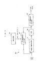
- Fig. 1 is a block diagram of the configuration of an analog-digital conversion circuit according to one embodiment of the invention.
- the analog-digital conversion circuit 100 in Fig. 1 includes a first stage circuit ST1, a second stage circuit ST2, switches SW1 and SW2, and a signal generator 30.
- the first stage circuit ST1 includes an operational amplifier 1, a sub A/D converter 7, a D/A converter 8, a subtraction circuit 5, and an operational amplifier 2.
- the subtraction circuit 5 and the operational amplifier 2 form a differential amplifier 2a.
- the second stage circuit ST2 includes an operational amplifier 3, a sub A/D converter 9, a D/A converter 10 , a subtraction circuit 6 , and an operational amplifier 4.
- the subtraction circuit 6 and the operational amplifier 4 form a differential amplifier 4a.
- the operational amplifiers 1 and 2 in the first stage circuit ST1 and the operational amplifiers 3 and 4 in the second stage circuit ST2 each have a gain of 2.
- the operational amplifier 1 may have a gain of 1.
- the sub A/D converter 7 in the first stage circuit ST1 has a 4-bit structure
- the sub A/D converter 9 in the second stage circuit ST2 has a structure of (two bits + one redundant bit). The redundant bit will not be taken into account in the following description.
- the signal generator 30 generates clock signals CLK1 and CLK3, and a control signal SW.
- the clock signal CLK1 has a frequency Fs
- the clock signal CLK3 has a frequency three times as high as the frequency Fs of the clock signal CLK1, i.e. 3Fs .
- the control signal SW has a frequency equal to the frequency Fs of the clock signal CLK1.
- the operational amplifier 1, the sub A/D converter 7, the D/A converter 8, and the operational amplifier 2 in the first stage circuit ST1 operate in response to the clock signal CLK1.
- the operational amplifier 3, the sub A/D converter 9, the D/A converter 10, and the operational amplifier 4 in the second stage circuit ST2 operate in response to the clock signal CLK3.
- the switches SW1 and SW2 turn on and off in a complimentary manner to each other in response to the control signal SW.
- An analog signal Vin is applied to an input terminal In.
- the analog signal Vin at the input terminal In is input to the operational amplifier 1 and the sub A/D converter 7 in the first stage circuit ST1.
- the sub A/D converter 7 A/D-converts the analog signal Vin, outputs a 4-bit digital signal as the result of A/D conversion, and also applies the digital signal to the D/A converter 8.
- the D/A converter 8 D/A-converts the 4-bit digital signal applied from the sub A/D converter 7 and outputs an analog signal VDA.
- the operational amplifier 1 samples and amplifies the analog signal Vin at the input terminal In for output.
- the subtraction circuit 5 subtracts between the analog signal Vin output from the operational amplifier 1 and the analog signal VDA output from the D/A converter 8.
- the operational amplifier 2 amplifies the output signal from the subtraction circuit 5 and outputs the amplified signal as an analog signal Vout.
- the analog signal Vout output from the operational amplifier 2 is applied to an input node NI in the second stage circuit ST2 when the switch SW1 is in an on state.
- the analog signal at the input node NI is input to the operational amplifier 3 and the sub A/D converter 9 in the second stage circuit ST2.
- the sub A/D converter 9 A/D-converts the analog signal, outputs a 2-bit digital signal as the result of A/D conversion, and also applies the digital signal to the D/A converter 10.
- the D/A converter 10 D/A-converts the 2-bit digital signal applied from the sub A/D converter 9 and outputs a resulting analog signal.
- the operational amplifier 3 samples and amplifies the analog signal at the input node NI for output.
- the subtraction circuit 6 subtracts between the analog signal output from the operational amplifier 3 and the analog signal output from the D/A converter 10.
- the operational amplifier 4 amplifies the output signal from the subtraction circuit 6 and outputs a resulting analog signal.
- the analog signal output from the operational amplifier 4 is applied to the input node NI when the switch SW2 is in an on state.
- the second stage circuit ST2 corresponds to the first circuit
- the first stage circuit ST1 corresponds to the second circuit
- the switches SW1 and SW2 correspond to the selector
- the signal generator 30 corresponds to the control device.
- the sub A/D converter 9 corresponds to the first analog-digital converter, the D/A converter 10 to the first digital-analog converter, the operational amplifier 3 to the first operational amplifier, and the differential amplifier 4a to the first differential amplifier.
- the sub analog-digital converter 7 corresponds to the second analog-digital converter, the D/A converter 8 to the second digital-analog converter, the operational amplifier 1 to the second operational amplifier, and the differential amplifier 2a to the second differential amplifier.
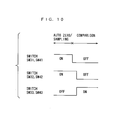
- FIG. 2 is a timing chart for use in illustration of the operation of the analog-digital conversion circuit 100 in Fig. 1.
- AMP represents amplifying operation
- AZ auto zero operation represents amplifying operation
- SMP sampling operation is the operation of nullifying the potential difference between the pair of input terminals of an operational amplifier.
- control signal SW attains a low level. This turns off the switch SW1 and turns on the switch SW2.
- the clock signal CLK1 attains a high level.
- the operational amplifier 1 in the first stage circuit ST1 carries out amplifying operation.
- the sub A/D converter 7 carries out A/D conversion operation. In this way, the sub A/D converter 7 outputs digital signals D9 to D6 of the high order 4 bits.
- the operational amplifier 2 carries out auto zero operation or sampling operation.
- the output of the D/A converter 8 is indefinite.
- the clock signal CLK1 attains a low level.
- This causes the operational amplifier 1 in the first stage circuit ST1 to carry out auto zero operation and sampling operation and the sub A/D converter 7 to carry out auto zero operation and sampling operation.
- the operational amplifier 2 carries out amplifying operation and the D/A converter 8 carries out D/A conversion operation.
- the analog signal output from the D/A converter 8 is definite.
- the control signal SW attains a high level. This turns on the switch SW1 and turns off the switch SW2. Consequently, the analog signal output from the operational amplifier 2 in the first stage circuit ST1 is applied to the input node NI in the second stage circuit ST2 through the switch SW1.
- the clock signal CLK3 attains a high level. This causes the operational amplifier 3 in the second stage circuit ST2 to carry out auto zero operation and sampling operation, and the sub A/D converter 9 to carry out auto zero operation and sampling operation. At the time, the operational amplifier 4 carries out amplifying operation, and the D/A converter 10 carries out D/A conversion operation.
- the clock signal CLK3 attains a low level.
- This causes the operational amplifier 3 in the second stage circuit ST2 to carry out amplifying operation and the sub A/D converter 9 to carry out A/D conversion operation.
- digital signals D5 and D4 of the intermediate high order 2 bits are output from the sub A/D converter 9.
- the operational amplifier 4 carries out auto zero operation and sampling operation, and the output of the D/A converter 10 is indefinite.
- the control signal SW attains a low level. This turns off the switch SW1, and turns on the switch SW2. Consequently, the analog signal output from the operational amplifier 4 in the second stage circuit ST2 to the output node NO is applied to the input node NI through the switch SW2.
- the clock signal CLK3 attains a high level. This causes the operational amplifier 3 in the second stage circuit ST2 to carry out auto zero operation and sampling operation, and the sub A/D converter 9 to carry out auto zero operation and sampling operation. At the time , the operational amplifier 4 carries out amplifying operation, and the D/A converter 10 carries out D/A conversion operation. Consequently, the analog signal output from the operational amplifier 4 to the output node NO is applied to the node NI through the switch SW2.
- the clock signal CLK3 attains a low level.
- This causes the operational amplifier 3 in the second stage circuit ST2 to carry out amplifying operation, and the sub A/D converter 9 to carry out A/D conversion operation.
- digital signals D3 and D2 of the intermediate low order 2 bits are output from the A/D converter 9.
- the operational amplifier 4 carries out auto zero operation and sampling operation, and the output of the D/A converter 10 is indefinite.
- the clock signal CLK3 attains a high level. This causes the operational amplifier 3 in the second stage circuit ST2 to carry out auto zero operation and sampling operation and the sub A/D converter 9 to carry out auto zero operation and sampling operation.
- the operational amplifier 4 carries out amplifying operation, and the D/A converter 10 carries out D/A conversion operation. Consequently, the analog signal output to the output node NO from the operational amplifier 4 is applied to the input node NI through the switch SW2.
- the clock signal CLK3 attains a low level.
- the operational amplifier 3 in the second stage circuit ST2 carries out amplifying operation, and the sub A/D converter 9 carries out A/D conversion operation.
- digital signals D1 and D0 of the low order 2 bits are output from the sub A/D converter 9.
- the operational amplifier 4 carries out auto zero operation and sampling operation, and the output of the D/A converter 10 is indefinite.
- the digital signals D9 to D6 of the high order 4 bits are output from the first stage circuit ST1.
- the digital signals D5 and D4 of the intermediate high order 2 bits, the digital signals D3 and D2 of the intermediate low order 2 bits, and the digital signals D1 and D0 of the low order 2 bits are sequentially output from the second stage circuit ST2.
- the 10-bit, four-stage pipeline structure is made of the two stages of circuits ST1 and ST2. Consequently, the necessary area is reduced.
- Fig. 3 is a block diagram of the configuration of an analog-digital conversion circuit according to another embodiment of the invention.
- the analog-digital conversion circuit 100a in Fig. 3 includes a circuit ST0, switches SW1 and SW2, and a signal generator 30.
- the circuit ST0 includes an operational amplifier 11, a sub A/D converter 14 , a D/A converter 15 , a subtraction circuit 13, and an operational amplifier 12 .
- the subtraction circuit 13 and the operational amplifier 12 form a differential amplifier 12a.
- the operational amplifiers 11 and 12 in the circuit ST0 each have a gain of 4.
- the sub A/D converter 14 in the circuit ST0 has a 4-bit structure.
- the signal generator 30 generates clock signals CLK1 and CLK3, and a control signal SW.
- the clock signal CLK1 has a frequency Fs
- the clock signal CLK3 has a frequency 3Fs, i.e., a frequency three times as high as the frequency Fs of the clock signal CLK1.
- the control signal SW has a frequency equal to the frequency Fs of the clock signal CLK1.
- the operational amplifier 11, the sub A/D converter 14, the D/A converter 15, and the operational amplifier 12 in the circuit ST0 operate in response to the clock signal CLK3.
- the switches SW1 and SW2 turn on and off in a complimentary manner to each other in response to the control signal SW.
- An analog signal Vin is applied to the input terminal In.
- the analog signal Vin at the input terminal In is input to the operational amplifier 11 and the sub A/D converter 14 in the circuit STO when the switch SW1 is in an on state.
- the sub A/D converter 14 A/D-converts the analog signal Vin, outputs a 4-bit digital signal as the result of A/D conversion, and also applies the digital signal to the D/A converter 15.
- the D/A converter 15 D/A-converts the 4-bit digital signal applied from the sub A/D converter 14 and outputs a resulting analog signal.
- the operational amplifier 11 samples and amplifies the analog signal at the input node NI for output.
- the subtraction circuit 13 subtracts between the analog signal output from the operational amplifier 11 and the analog signal output from the D/A converter 15.
- the operational amplifier 12 amplifies the output signal from the subtraction circuit 13 and outputs a resulting analog signal.
- the analog signal output from the operational amplifier 12 is applied to the input node NI when the switch SW2 is in an on state.
- the circuit ST0 corresponds to the f irst circuit
- the switches SW1 and SW2 correspond to the selector.
- the signal generator 30 corresponds to the control device.
- the sub A/D converter 14 corresponds to the first analog-digital converter, the D/A converter 15 to the first digital-analog converter, the operational amplifier 11 to the first operational amplifier, and the differential amplifier 12a to the first differential amplifier.
- FIG. 4 is a timing chart for use in illustration of the operation of the analog-digital conversion circuit 110a in Fig. 3.
- AMP represents amplifying operation, AZ auto zero operation, and SMP sampling operation.
- the control signal SW attains a high level. This turns on the switch SW1 and turns off the switch SW2. Therefore, the analog signal Vin applied to the input terminal In is applied to the input node NI through the switch SW1.
- the clock signal CLK3 attains a high level. This causes the operational amplifier 11 in the circuit ST0 to carry out auto zero operation and sampling operation.
- the sub A/D converter 14 carries out auto zero operation and sampling operation.
- the operational amplifier 12 carries out amplifying operation.
- the output of the D/A converter 15 is indefinite.
- the clock signal CLK3 attains a low level .
- This causes the operational amplifier 11 in the circuit STO to carry out amplifying operation, and the sub A/D converter 14 to carry out A/D conversion operation.
- digital signals D9 to D6 of the high order 4 bits are output from the sub A/D converter 14.
- the clock signal CLK3 attains a high level. This causes the operational amplifier 11 in the circuit ST0 to carry out auto zero operation and sampling operation, and the sub A/D converter 14 to carry out auto zero operation and sampling operation. At the time, the operational amplifier 12 carries out amplifying operation, and the D/A converter 15 carries out D/A conversion operation. As a result, the analog signal output to the output node NO from the operational amplifier 12 is applied to the input node NI through the switch SW2.
- the clock signal CLK3 attains a low level.
- This causes the operational amplifier 11 in the circuit ST0 to carry out amplifying operation and the sub A/D converter 14 to carry out A/D conversion operation.
- digital signals D5 to D3 of the intermediate order 3 bits and one redundant bit are output from the sub A/D converter 14.
- the operational amplifier 12 carries out auto zero operation and sampling operation, and the output of the D/A converter 15 is indefinite.
- the clock signal CLK3 attains a high level.
- the sub A/D converter 14 carries out auto zero operation and sampling operation.
- the operational amplifier 12 carries out amplifying operation, and the D/A converter 15 carries out D/A conversion operation. Consequently, the analog signal output from the operational amplifier 12 to the output node NO is applied to the input node NI through the switch SW2.
- the clock signal CLK3 attains a low level. This causes the operational amplifier 11 in the circuit ST0 to carry out amplifying operation, and the sub A/D converter 14 to carry out A/D conversion operation. At the time, digital signals D2 to D0 of the low order 3 bits and one redundant bit are output from the sub A/D converter 14. At the time, the operational amplifier 12 carries out auto zero operation and sampling operation, and the output of the D/A converter 15 is indefinite.
- the digital signals D9 to D6 of the high order 4 bits, the digital signals D5 to D3 of the intermediate order 3 bits, and the digital signals D2 to D0 of the low order 3 bits are sequentially output from the single circuit ST0.
- the 10-bit, three-stage pipeline structure is made of the single stage circuit ST0. Consequently, the necessary area is reduced.
- the circuits ST1, ST2, and ST0 in the corresponding stages, the pairs of operational amplifiers 1 and 2, 3 and 4, and 11 and 12 are provided, respectively. Meanwhile, a single operational amplifier or three or more operational amplifiers may be provided in the circuit in each stage.
- Fig. 5 is a block diagram of the configuration of a main part of the signal generator 30 in the analog-digital conversion circuits 100 and 100a in Figs. 1 and 3, respectively.
- the signal generator 30 in Fig. 5 includes a phase comparator 31, a VCO (Voltage-Controlled Oscillator) 32, a 1/N frequency divider 33, a 1/2 frequency divider 34, and a register 35.
- the register 35 stores a value N in advance.
- the value N is an arbitrary positive integer.
- a control signal RC to set the value N is applied to the 1/N frequency divider 33 from the register 35.
- the phase comparator 31 compares the phase of the clock signal CLK1 at a frequency Fs and the phase of the output signal of the 1/N frequency divider 33, and applies control voltage corresponding to the phase difference to the VCO 32.
- the VCO 32 outputs an oscillation signal having a frequency corresponding to the control voltage to the 1/2 frequency divider 34 and the 1/N frequency divider 33.
- the 1/N frequency divider 33 frequency-divides the oscillation signal output from the VCO 32 by N and applies the 1/N-frequency-divided oscillation signal to the phase comparator 31.
- the 1/2 frequency divider 34 frequency-divides the oscillation signal output from VCO 32 by 2 and outputs the 1/2 frequency-divided oscillation signal as a clock signal CLKn.
- the first stage circuit ST1 has a 4-bit structure
- the second stage circuit ST2 has a structure of (two bits + one redundant bit), and thus a 6-bit pipeline structure is formed.
- the first stage circuit ST1 has a 4-bit structure
- the second stage circuit ST2 has a structure of (two bits + one redundant bit) in the first and second cycles. In this way, an 8-bit pipeline structure is formed.
- the first stage circuit ST1 has a 4-bit structure
- the second stage circuit ST2 has a structure of (two bits + one redundant bit) in the first to fourth cycles. In this way, a 12-bit pipeline structure is formed.
- the circuit ST0 has a 4-bit structure, and a 4-bit pipeline structure is formed.
- the circuit ST0 has a 4-bit structure in the first cycle and a structure of (three bits + one redundant bit) in the second cycle, and a 7-bit pipeline structure is formed.
- the circuit ST0 has a 4-bit structure in the first cycle and a structure of (three bits + one redundant bit) in the second to fourth cycles. In this way, a 13-bit pipeline structure is formed.
- phase comparator 31, the VCO 32, and the 1/N frequency divider 33 form a phase locked loop, and the 1/N frequency divider 33 corresponds to the frequency divider 33.
- the register 35 corresponds to the frequency dividing factor setting device.
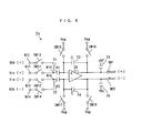
- Fig. 6 is a circuit diagram of a differential amplifier 2a in the analog-digital conversion circuit 100 in Fig . 1. Note that the differential amplifier 2a in Fig. 6 is a fully differential type, subtracting amplifying circuit.
- a capacitor 21 is connected between the non-inverting input terminal of the operational amplifier 20 and a node N15, and a capacitor 22 is connected between the inverting input terminal and a node N16.
- the node N15 is connected to nodes N11 and N13 through switches SW11 and SW13, respectively.
- the node N16 is connected to nodes N12 and N14 through switches SW12 and SW14, respectively.
- the operational amplifier 20 has its inverting output terminal connected to a node NO1 and its non-inverting input terminal through a capacitor 23.
- the operational amplifier 20 has its non-inverting output terminal connected to a node NO2 and its inverting input terminal through a capacitor 24.
- the operational amplifier 20 has its non-inverting input terminal connected to a reference terminal that receives reference voltage Vag through a switch SW15 and its inverting input terminal connected to the reference terminal through a switch SW17.
- the operational amplifier 20 has its inverting output terminal connected to the reference terminal through the switch SW16 and its non-inverting output terminal connected to the reference terminal through a switch SW18.
- the nodes NO1 and NO2 are grounded through capacitors 25 and 26, respectively.
- the switches SW11 to SW18 are each made of a CMOS switch. These switches SW1 to SW18 are controlled in response to a control signal SW or the inverted signal thereof.
- the differential amplifier 2a is provided with the analog signal Vin at the input terminal In and the analog signal VDA resulting from the D/A conversion by the D/A converter 8. More specifically, analog signals Vine +) and Vine -) are applied to the nodes N11 and N12, respectively.
- Vin Vin(+)-Vin(-) stands.
- Analog signals VDA(+) and VDA(-) are applied to the nodes N13 and N14, respectively.
- VDA VDA(+) - VDA(-) stands.
- Analog signals Vout (+) and Vout(-) appear at the nodes NO1 and NO2 , respectively.
- Vout Vout(+) - Vout(-) stands.
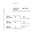
- Fig. 7 is a timing chart for use in illustration of the operation of the differential amplifier 2a in Fig. 6.
- the capacitance values of the capacitors 23 and 24 are each C
- the capacitance values of the capacitors 21 and 22 are each KC.
- K is a constant.
- the switches SW11, SW12 , and SW15 to SW18 turn on, while the switches SW13 and SW14 turn off.
- the non-inverting and inverting input terminals of the operational amplifier 20 are brought to an equal potential, and the inverting and non-inverting output terminals are brought to an equal potential.
- the analog signal Vin(+) is input to the node N15 through the switch SW11, and the analog signal Vin(-) is input to the node N16 through the switch SW12. More specifically, the analog signals Vin(+) and Vin(-) are sampled.
- the switches SW13 and SW14 turn on. This allows the analog signal VDA(+) to be input to the node N15 through the switch SW13 and the analog signal VDA(-) to be input to the node N16 through the switch SW14. Consequently, the difference between the analog signals Vin(+) and VDA(+) is amplified by K times, and the difference between the analog signals Vin(-) and VDA(-) is amplified by K times. As a result, the analog signal Vout (+) appears at the node NO1, and the analog signal Vout(-) appears at the node NO2.
- Fig. 8 is a circuit diagram of the configuration of the sub A/D converter 7 in the analog-digital conversion circuit 100 in Fig. 1.
- the sub A/D converter 7 in Fig. 8 is an full parallel comparison (flush) type sub A/D converter.
- the sub A/D converter 7 in Fig. 8 includes n resistors R, n voltage comparators D1 to Dn and an encoder 70.
- All the resistors R have the same resistance value and are connected in series between a node N31 that receives high potential side reference voltage VRT and a node N32 that receives low potential side reference voltage VRB.
- the potentials at nodes N41 to N4n between the n resistors R between the node N32 and N31 are VR(1) to VR(n), respectively.
- An analog signal Vin is input to the non-inverting input terminals of the voltage comparators D1 to Dn.
- the potentials VR(1) to VR(n) at the nodes N41 to N4n are applied to the inverting input terminals of the voltage comparators D1 to Dn, respectively.
- the output signals VD1 to VDn of the voltage comparators D1 to Dn attain a high level when the analog signal Vin is higher than the potentials VR(1) to VR(n) .
- These signals attain a low level when the analog signal Vin is lower than the potentials VR(1) to VR(n).
- the encoder 70 encodes the output signals VD1 to VDn of the voltage comparators D1 to Dn and outputs a 4-bit digital signal Dout.
- Fig. 9 is a circuit diagram of a differential voltage comparator used in the sub A/D converter 7 in Fig. 8.
- a differential amplifying circuit 50 includes P-channel MOS field effect transistors (hereinafter referred to as "PMOS transistors”) 51 and 52, N-channel MOS field effect transistors (hereinafter referred to as “NMOS transistors”) 53 and 54, and a constant current source 57.
- PMOS transistors P-channel MOS field effect transistors
- NMOS transistors N-channel MOS field effect transistors
- a saturation NMOS transistor is used for the constant current source 57.
- the PMOS transistor 51 is connected between a node ND and an output node NO11, and the PMOS transistor 52 is connected between the node ND and an output node NO12.
- the NMOS transistor 53 is connected between the output node NO11 and a node NS, and the NMOS transistor 54 is connected between the output node NO12 and the node NS.
- the node ND is provided with power supply voltage V DD and the node NS is grounded through the constant current source 57.
- the PMOS transistors 51 and 52 have their gates provided with bias voltage V B .
- the NMOS transistors 53 and 54 have their gates connected to input nodes NA and NB, respectively.
- the input node NA is connected to the node N1 through a capacitor 55, and the input node NB is connected to a node N2 through a capacitor 56.
- a switch SW31 is connected between the input node NA and the output node NO11, and a switch SW41 is connected between the input node NB and the output node NO12 .
- Switches SW32 and SW33 are connected in parallel to the node N1, and switches SW42 and SW43 are connected in parallel to the node N2.
- the switches SW31 to SW33, and the switches SW41 to SW43 are each made of a CMOS switch. These switches are controlled in response to the control signal SW or the inverted signal thereof.
- Input voltages V 1 (+) and V 2 (+) are applied to the input ends of the switches SW32 and SW33, respectively and input voltages V 1 (-) and V 2 (-) are applied to the input ends of the switches SW42 and SW43, respectively.
- Output voltages V o (+) and V o (-) are led from the output nodes NO11 and NO12.
- the difference between the input voltages V 1 (+) and V 2 (+) is the differential input voltage V(+)
- the difference between the input voltages V 1 (-) and V 2 (-) is the differential input voltage V(-).
- the difference between the output voltages V o (+) and V o (-) is the differential output voltage V o .
- the analog signal Vin in Fig. 8 corresponds to the differential input voltage V(+)
- any of the potentials VR(1) to VR(n) corresponds to the differential input voltage V(-).
- Any of the output signals VD1 to VDn corresponds to the differential output voltage V o .
- Fig. 10 is a timing chart for use in illustration of the operation of the voltage comparator in Fig. 9.
- the switches SW31, SW41, SW32, and SW42 turn on, and the switches SW33 and SW43 turn off.
- the input node NA and the output node NO11 are brought to an equal potential
- the input node NB and the output node NO12 are brought to an equal potential.
- the input voltage V 1 (+) is input to the input node NA through the switch SW32 and the input voltage V 1 (-) is input to the input node NB through the switch SW42. More specifically, the input voltages V 1 (+) and V 1 (-) are sampled.
- the switches SW33 and SW43 turn on. Then, the input voltage V 2 (+) is input to the input node NA through the switch SW33, and the input voltage V 2 (-) is input to the input node NB through the switch SW43. Consequently, the voltage change at the input node NA equals to V 2 (+)-V 1 (+). and the voltage change at the input node NB equals to V 2 (-)-V 1 (-).
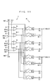
- Fig. 11 is a circuit diagram of the sub A/D converter 7 and the D/A converter 8 in the analog-digital conversion circuit 10 in Fig. 1.
- the D/A converter 8 is a capacitor array type, D/A converter. Note that the encoder 70 in Fig. 8 is not shown in Fig. 11.
- the D/A converter 8 includes sets of n switches E1 to En, F1 to Fn, G1 to Gn, and H1 to Hn (each set of switches connected in an array), n positive side capacitors B1 to Bn, and n negative side capacitors C1 to Cn.
- the capacitors B1 to Bn and C1 to Cn all have the same capacitance value c.
- the differential positive side output voltage VDA(+) is generated from the terminals on one side of the capacitors B1 to Bn (hereinafter referred to as "output terminals")
- the differential negative side output voltage VDA(-) is generated from the terminals on one side of the capacitors C1 to Cn (hereinafter referred to as "output terminals").
- the other terminals of the capacitors B1 to Bn and C1 to Cn are referred to as "input terminals.”
- the terminals on one side of the switches E1 to En are connected to the node N31, and the other terminals are connected to the input terminals of the capacitors B1 to Bn, respectively.
- the terminals on one side of the switches F1 to Fn are connected to the node N31 and the other terminals are connected to the input terminals of the capacitors C1 to Cn .
- the terminals on one side of the switches G1 to Gn are connected to the node N32, and the other terminals are connected to the input terminals of the capacitors B1 to Bn.
- the terminals on one side of the switches H1 to Hn are connected to the node N32, and the other terminals are connected to the input terminals of the capacitors C1 to Cn.
- switches E1 to En, F1 to Fn, G1 to Gn, and H1 to Hn those with the same suffix number form a quadruple switch.
- the switches E1, F1, G1, and H1 form one
- the switches En, Fn, Gn, and Hn form another.
- the switches E1 to En, F1 to Fn, G1 to Gn, and H1 to Hn turn on/off in response to the output levels of the voltage comparators D1 to Dn, respectively. For example, when the output of the voltage comparator Dn is in a high level, the switches En and Hn turn on, and the switches Gn and Fn turn off. Conversely, when the output of the voltage comparator Dn is in a low level, the switches En and Hn turn off, and the switches Gn and Fn turn on.
- VDA (+) VRB+m(VRT-VRB)/n
- VDA(-) VRT-m(VRT-VRB)/n
- the circuits 100 and 100a As in the foregoing, in the analog-digital conversion circuits 100 and 100a according to the embodiment, the necessary area is reduced, and various bit structures can be implemented by the same hardware structure. Therefore, the circuit is most suitably applied to an embedded type analog-digital conversion circuit.
Landscapes
- Engineering & Computer Science (AREA)
- Theoretical Computer Science (AREA)
- Analogue/Digital Conversion (AREA)
Applications Claiming Priority (2)
| Application Number | Priority Date | Filing Date | Title |
|---|---|---|---|
| JP2002258058A JP2004096636A (ja) | 2002-09-03 | 2002-09-03 | アナログ−デジタル変換回路 |
| JP2002258058 | 2002-09-03 |
Publications (2)
| Publication Number | Publication Date |
|---|---|
| EP1398880A2 true EP1398880A2 (de) | 2004-03-17 |
| EP1398880A3 EP1398880A3 (de) | 2006-04-26 |
Family
ID=31884709
Family Applications (1)
| Application Number | Title | Priority Date | Filing Date |
|---|---|---|---|
| EP03255510A Withdrawn EP1398880A3 (de) | 2002-09-03 | 2003-09-03 | Schaltung zur Analog-Digital-Wandlung |
Country Status (4)
| Country | Link |
|---|---|
| US (1) | US6859158B2 (de) |
| EP (1) | EP1398880A3 (de) |
| JP (1) | JP2004096636A (de) |
| CN (1) | CN100334809C (de) |
Families Citing this family (12)
| Publication number | Priority date | Publication date | Assignee | Title |
|---|---|---|---|---|
| JP4014553B2 (ja) * | 2003-09-29 | 2007-11-28 | 三洋電機株式会社 | アナログデジタル変換器 |
| US7095352B2 (en) * | 2004-03-02 | 2006-08-22 | Sanyo Electric Co., Ltd. | Analog-to-digital converter including a plurality of amplifier circuits |
| JP4093976B2 (ja) * | 2004-03-17 | 2008-06-04 | 三洋電機株式会社 | アナログデジタル変換器 |
| JP3785175B2 (ja) * | 2004-03-30 | 2006-06-14 | 株式会社東芝 | 多入力a/d変換装置及びこれを用いた無線受信機 |
| US7193553B1 (en) * | 2004-12-07 | 2007-03-20 | National Semiconductor Corporation | Analog to digital converter with power-saving adjustable resolution |
| JP2006173807A (ja) * | 2004-12-13 | 2006-06-29 | Sanyo Electric Co Ltd | アナログデジタル変換器 |
| JP2007208422A (ja) * | 2006-01-31 | 2007-08-16 | Sanyo Electric Co Ltd | アナログデジタル変換器 |
| US7397412B1 (en) * | 2006-02-03 | 2008-07-08 | Marvell International Ltd. | Low power analog to digital converter |
| US8553827B2 (en) * | 2009-10-20 | 2013-10-08 | Qualcomm Incorporated | ADC-based mixed-mode digital phase-locked loop |
| EP2677661A4 (de) | 2011-02-18 | 2017-08-23 | National University Corporation Shizuoka University | A/d-wandler, bildsensorvorrichtung und verfahren zur erzeugung digitaler signale aus analogen signalen |
| US9043062B2 (en) * | 2012-10-05 | 2015-05-26 | Ford Global Technologies, Llc | Hybrid electric vehicle powertrain and control system |
| US10230384B2 (en) | 2016-12-09 | 2019-03-12 | Rambus Inc. | Variable resolution digital equalization |
Family Cites Families (7)
| Publication number | Priority date | Publication date | Assignee | Title |
|---|---|---|---|---|
| JP2689689B2 (ja) | 1990-05-22 | 1997-12-10 | 日本電気株式会社 | 直並列型アナログ/ディジタル変換器 |
| JP3153271B2 (ja) * | 1991-07-05 | 2001-04-03 | 株式会社日立製作所 | Ad変換器 |
| JP3581485B2 (ja) * | 1996-04-05 | 2004-10-27 | 株式会社ルネサステクノロジ | パイプライン型a/dコンバータ |
| US6304206B1 (en) * | 1997-09-04 | 2001-10-16 | Sanyo Electric Co., Ltd. | Voltage comparator, operational amplifier and analog-to-digital conversion circuit employing the same |
| JP3384717B2 (ja) | 1997-09-04 | 2003-03-10 | 三洋電機株式会社 | アナログ−デジタル変換回路 |
| US6097326A (en) * | 1998-05-26 | 2000-08-01 | National Semiconductor Corporation | Algorithmic analog-to-digital converter with reduced differential non-linearity and method |
| CN1285174C (zh) * | 2001-06-18 | 2006-11-15 | 三洋电机株式会社 | 模-数转换电路 |
-
2002
- 2002-09-03 JP JP2002258058A patent/JP2004096636A/ja active Pending
-
2003
- 2003-09-03 CN CNB031593186A patent/CN100334809C/zh not_active Expired - Fee Related
- 2003-09-03 US US10/653,251 patent/US6859158B2/en not_active Expired - Lifetime
- 2003-09-03 EP EP03255510A patent/EP1398880A3/de not_active Withdrawn
Also Published As
| Publication number | Publication date |
|---|---|
| JP2004096636A (ja) | 2004-03-25 |
| CN100334809C (zh) | 2007-08-29 |
| EP1398880A3 (de) | 2006-04-26 |
| US6859158B2 (en) | 2005-02-22 |
| CN1490936A (zh) | 2004-04-21 |
| US20040041722A1 (en) | 2004-03-04 |
Similar Documents
| Publication | Publication Date | Title |
|---|---|---|
| CN108574487B (zh) | 逐次逼近寄存器模数转换器 | |
| US5710563A (en) | Pipeline analog to digital converter architecture with reduced mismatch error | |
| US6683554B2 (en) | Analog-to-digital conversion circuit having increased conversion speed and high conversion accuracy | |
| US7030804B2 (en) | Switched-capacitor circuit and pipelined A/D converter | |
| US11296714B2 (en) | Residue transfer loop, successive approximation register analog-to-digital converter, and gain calibration method | |
| US9219489B2 (en) | Successive approximation register analog-to-digital converter | |
| US6900749B2 (en) | Analog-to-digital conversion circuit | |
| EP3567720B1 (de) | Fehlanpassungs- und referenzgleichtakt-offset-unempfindliche einseitig geschaltete kondensatorverstärkungsstufe | |
| US6229472B1 (en) | A/D converter | |
| US10804920B2 (en) | A/D converter | |
| KR101168047B1 (ko) | 파이프라인 아날로그-디지털 컨버터 및 그의 구동 방법 | |
| EP1398880A2 (de) | Schaltung zur Analog-Digital-Wandlung | |
| CN102751988A (zh) | 模拟数字转换器和信号处理系统 | |
| US7088277B2 (en) | Analog-to-digital converter having cyclic configuration | |
| US7224306B2 (en) | Analog-to-digital converter in which settling time of amplifier circuit is reduced | |
| KR100294787B1 (ko) | 개방루프차동증폭기를갖는서브레인지아날로그/디지털컨버터 | |
| US6977606B2 (en) | Pipelined analog-to-digital converter | |
| CN100486116C (zh) | 模数转换器 | |
| JP4684028B2 (ja) | パイプラインa/d変換器 | |
| JP5609522B2 (ja) | アナログデジタル変換器および信号処理システム | |
| JP2003008439A (ja) | アナログ−デジタル変換回路 | |
| JP3851305B2 (ja) | アナログ−デジタル変換回路 | |
| CN115276657A (zh) | 流水线型模数转换器 | |
| JPH11112305A (ja) | 電圧比較器、演算増幅器、アナログ−デジタル変換器およびアナログ−デジタル変換回路 | |
| JP2007325319A (ja) | アナログ−デジタル変換器 |
Legal Events
| Date | Code | Title | Description |
|---|---|---|---|
| PUAI | Public reference made under article 153(3) epc to a published international application that has entered the european phase |
Free format text: ORIGINAL CODE: 0009012 |
|
| AK | Designated contracting states |
Kind code of ref document: A2 Designated state(s): AT BE BG CH CY CZ DE DK EE ES FI FR GB GR HU IE IT LI LU MC NL PT RO SE SI SK TR |
|
| AX | Request for extension of the european patent |
Extension state: AL LT LV MK |
|
| PUAL | Search report despatched |
Free format text: ORIGINAL CODE: 0009013 |
|
| AK | Designated contracting states |
Kind code of ref document: A3 Designated state(s): AT BE BG CH CY CZ DE DK EE ES FI FR GB GR HU IE IT LI LU MC NL PT RO SE SI SK TR |
|
| AX | Request for extension of the european patent |
Extension state: AL LT LV MK |
|
| 17P | Request for examination filed |
Effective date: 20060801 |
|
| AKX | Designation fees paid |
Designated state(s): DE FR NL |
|
| 17Q | First examination report despatched |
Effective date: 20070402 |
|
| STAA | Information on the status of an ep patent application or granted ep patent |
Free format text: STATUS: THE APPLICATION HAS BEEN WITHDRAWN |
|
| 18W | Application withdrawn |
Effective date: 20080902 |