EP1400995A1 - Procede de production de condensateur electrolytique solide - Google Patents
Procede de production de condensateur electrolytique solide Download PDFInfo
- Publication number
- EP1400995A1 EP1400995A1 EP02743708A EP02743708A EP1400995A1 EP 1400995 A1 EP1400995 A1 EP 1400995A1 EP 02743708 A EP02743708 A EP 02743708A EP 02743708 A EP02743708 A EP 02743708A EP 1400995 A1 EP1400995 A1 EP 1400995A1
- Authority
- EP
- European Patent Office
- Prior art keywords
- forming
- solid electrolytic
- hole
- layer
- aluminum foil
- Prior art date
- Legal status (The legal status is an assumption and is not a legal conclusion. Google has not performed a legal analysis and makes no representation as to the accuracy of the status listed.)
- Withdrawn
Links
Images






Classifications
-
- H—ELECTRICITY
- H01—ELECTRIC ELEMENTS
- H01G—CAPACITORS; CAPACITORS, RECTIFIERS, DETECTORS, SWITCHING DEVICES, LIGHT-SENSITIVE OR TEMPERATURE-SENSITIVE DEVICES OF THE ELECTROLYTIC TYPE
- H01G9/00—Electrolytic capacitors, rectifiers, detectors, switching devices, light-sensitive or temperature-sensitive devices; Processes of their manufacture
- H01G9/15—Solid electrolytic capacitors
-
- Y—GENERAL TAGGING OF NEW TECHNOLOGICAL DEVELOPMENTS; GENERAL TAGGING OF CROSS-SECTIONAL TECHNOLOGIES SPANNING OVER SEVERAL SECTIONS OF THE IPC; TECHNICAL SUBJECTS COVERED BY FORMER USPC CROSS-REFERENCE ART COLLECTIONS [XRACs] AND DIGESTS
- Y10—TECHNICAL SUBJECTS COVERED BY FORMER USPC
- Y10T—TECHNICAL SUBJECTS COVERED BY FORMER US CLASSIFICATION
- Y10T29/00—Metal working
- Y10T29/43—Electric condenser making
-
- Y—GENERAL TAGGING OF NEW TECHNOLOGICAL DEVELOPMENTS; GENERAL TAGGING OF CROSS-SECTIONAL TECHNOLOGIES SPANNING OVER SEVERAL SECTIONS OF THE IPC; TECHNICAL SUBJECTS COVERED BY FORMER USPC CROSS-REFERENCE ART COLLECTIONS [XRACs] AND DIGESTS
- Y10—TECHNICAL SUBJECTS COVERED BY FORMER USPC
- Y10T—TECHNICAL SUBJECTS COVERED BY FORMER US CLASSIFICATION
- Y10T29/00—Metal working
- Y10T29/49—Method of mechanical manufacture
- Y10T29/49002—Electrical device making
- Y10T29/49117—Conductor or circuit manufacturing
- Y10T29/49124—On flat or curved insulated base, e.g., printed circuit, etc.
- Y10T29/49128—Assembling formed circuit to base
-
- Y—GENERAL TAGGING OF NEW TECHNOLOGICAL DEVELOPMENTS; GENERAL TAGGING OF CROSS-SECTIONAL TECHNOLOGIES SPANNING OVER SEVERAL SECTIONS OF THE IPC; TECHNICAL SUBJECTS COVERED BY FORMER USPC CROSS-REFERENCE ART COLLECTIONS [XRACs] AND DIGESTS
- Y10—TECHNICAL SUBJECTS COVERED BY FORMER USPC
- Y10T—TECHNICAL SUBJECTS COVERED BY FORMER US CLASSIFICATION
- Y10T29/00—Metal working
- Y10T29/49—Method of mechanical manufacture
- Y10T29/49002—Electrical device making
- Y10T29/49117—Conductor or circuit manufacturing
- Y10T29/49124—On flat or curved insulated base, e.g., printed circuit, etc.
- Y10T29/49155—Manufacturing circuit on or in base
- Y10T29/49165—Manufacturing circuit on or in base by forming conductive walled aperture in base
Definitions
- the present invention relates to a method for manufacturing solid electrolytic capacitor for use in various kinds of electronic apparatus.
- capacitors are requested to be compact yet to have a larger capacitance, a lower ESR (Equivalent Series Resistance) and a lower ESL (Equivalent Series Inductance).
- the USP 5377073 and the Japanese Patent Laid-open No. H11-274002 disclose a technology of laminating capacitor elements in a chip-type capacitor.
- the conventional SECs can be increased in the capacitance, and improved in the ESR.
- the SECs when mounting the conventional SECs on the surface of a circuit board like semiconductor components, the SECs need the help of external terminals for connection. This way of connection poses a limitation in the improvement of ESL. In order to further reduce the ESL, shapes and length of terminals for electrical connection and the wirings need to be streamlined.
- the present invention addresses the above problems, and aims to offer a method for manufacturing large capacitance SECs that can be connected direct with semiconductor components and implement a superior high frequency response.
- a method for manufacturing SEC in accordance with the present invention comprises the steps of forming a porous portion on one of the surfaces of an aluminum foil, forming a dielectric layer on said porous portion, forming a through hole at a certain specific location of said aluminum foil, forming an insulation layer on said aluminum foil covering the other surface which is opposite to the one having said porous portion and the inner wall surface of said through hole, forming a solid electrolytic layer on said dielectric layer, forming a through hole electrode in said through hole, forming a collector layer on said solid electrolytic layer, forming an opening at a certain specific location of said insulating layer provided on said aluminum foil, and forming a connection terminal in said opening and on the exposed surface of said through hole electrode. Since the connection terminals provided in the opening of insulation layer and on the exposed surface of through hole electrode are disposed on a same plane, the SEC can be connected direct with semiconductor component and offers a superior high frequency characteristic.
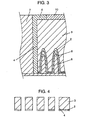
- FIG. 1 - FIG. 3 in a sheet-formed capacitor element 1, one of the surfaces of an aluminum foil 3 is made porous by etching or the like process, a dielectric layer 2 is formed on the porous portion, and a through hole 4 is formed in the aluminum foil 3 at a certain specific location.
- An insulation layer 5 is provided to cover the other surface, viz. non-porous surface, of the aluminum foil 3 and the inner wall surface of through hole 4, and a solid electrolytic layer 6 is formed on the dielectric layer 2.
- a through hole electrode 7 is formed in the through hole 4, and then a collector layer 8 is formed on the solid electrolytic layer 6.
- the insulation layer 5 on aluminum foil 3 is provided with an opening 9 at a certain specific location, and the surface exposed by the opening 9 is provided with a connection terminal 10.
- the through hole electrode refers to an electrode formed in the through hole.
- the capacitor element 1 thus structured is provided with a package 11 covering the side surfaces and the collector layer 8.
- a first external terminal 12, which is electrically connected with the aluminum foil 3, and a second external terminal 13, which is electrically connected with the collector layer 8, are provided on the package 11, and then a connection bump 14 is provided on the through hole electrode 7 and the connection terminal 10, respectively.
- a finished SEC is thus completed.
- a method for manufacturing SEC in the present invention is described referring to the drawings FIG. 4 through FIG. 12.
- the aluminum foil 3 with dielectric layer 2 is provided by etching one of the surfaces of an aluminum foil 3 to make it porous, and then forming a dielectric oxide film thereon through anode oxidization in a electrolytic solution. And then, the aluminum foil 3 is provided with a through hole 4 at a certain specific location, as shown in FIG. 4.
- the through holes can be formed altogether by means of a wet etching process. Besides the wet etching, a finer through hole of 100 ⁇ m or smaller can be formed at a high precision level by using a laser beam machining, a punching method, a drilling method, an electric discharge machining, or the like means. The above methods are applicable to any kinds of materials.
- a wet etching process an aluminum foil 3 is etched after the foil is provided at both surfaces with resist film having openings at places corresponding to the through holes, and then the resist film is removed.
- edge of the through hole at the surface to be facing to dielectric layer 2 is chamfered by means of wet etching or the like process, it contributes to further improve the reliability of an insulation layer, which will be provided at a later step.
- an insulation layer 5 is formed to cover the other surface, viz. non-porous surface, of the aluminum foil 3 and the inner wall surface of through hole 4, as shown in FIG. 5.
- the electrodeposition provides an even and intense insulation layer, there is a possibility that the thickness of the layer turns out to be slightly thinner at the edge of through hole 4 facing the dielectric layer 2.
- the edge chamfering is effective for eliminating the risk and implementing a higher insulating reliability.
- an insulating resin containing a micro gel of high edge-covering property, carbon particles and titanium oxide particles through electrodeposition is quite advantageous.
- the micro gel referred to in the present example is a polymer added with a polymer substance of particle diameter 10 ⁇ m or smaller to increase the viscosity and lower the fluidity; thereby improving the edge-covering property.
- a resin mixture of high edge-covering property is electrodeposited onto the inner wall surface of fine through hole of 100 ⁇ m or smaller, the deposited layer may become too thick and clog the through hole.
- a solid electrolytic layer 6 is formed on the dielectric layer 2.
- the solid electrolytic layer 6 can be formed through a chemical polymerization or an electrolytic polymerization of a ⁇ electron conjugated polymer such as polypyrrole, polythiophene, and/or a composite material containing a conducting polymer other than that; or by combining these.
- the process can be formed by applying a suspension of conducting polymer and drying it, and then conducting an electrolytic polymerization; or, by impregnating it with manganese nitrate and then heat-decomposing it to generate manganese dioxide, and then conducting an electrolytic polymerization.
- a further established technology available for forming a solid electrolytic layer is forming manganese dioxide by heat-decomposing manganese nitrate.
- the through hole is filled with a conducting adhesive substance such as Ag paste, Cu paste, etc. containing conductive particles; and then it is cured to form the through hole electrode 7.
- a collector layer 8 is formed on the solid electrolytic layer 6, as shown in FIG. 8.
- the collector layer 8 is formed by using a suspension of carbon particles and a conducting adhesive material containing a silver past as the main ingredient, into a laminate structure of a carbon layer and a silver paste layer. The structure efficiently makes the electrical charges available. Then, as shown in FIG.
- the insulation layer 5 formed on the other surface of aluminum foil 3 is provided with an opening 9 at a certain specific location, by means of YAG laser or other process such as grinding.
- the opening 9 can be formed also by other process; namely, providing a resist portion on the aluminum foil 3 before formation of insulation layer 5 at a certain specific place on the non-porous surface, and forming a collector layer 8 and an insulation layer 5, and then removing the resist portion.
- a connection terminal 10 is formed on the surface exposed through the opening 9 of insulation layer 5, as shown in FIG. 10, using a conductive adhesive substance, or by an electroplating or electroless plating.
- the capacitor element 1 is covered with an epoxy resin package 11, as shown in FIG.
- the package 11 for protecting it from humidity and stress from outside and ensuring good electrical insulation and increasing the reliability.
- the package 11 is provided with a first external terminal 12, which is electrically connected with the aluminum foil 3, and a second external terminal 13, which is electrically connected with the collector layer 8, to complete a finished capacitor element 1.
- connection bumps 14 on the connection terminal 10 and the through hole electrode 7, in order to raise the reliability in electrical connection with a semiconductor component or the like electronic component, and to improve the electrical performance.
- connection terminals 10 and the connection bumps 14 disposed respectively on a same plane.
- present invention offers a method for manufacturing SECs that can be connected direct with semiconductor components, and superior in the high frequency characteristic.
- FIG. 13 and FIG. 14 are the drawings used to describe the main process steps of manufacturing an SEC in accordance with a second exemplary embodiment of the present invention.
- an aluminum foil 3 is etched for making it porous, and a dielectric layer 2 is formed on the porous portion. And then, a through hole 4 is formed in the aluminum foil 3 at a certain specific location, and an insulation layer 5 is provided to cover the other surface, viz. non-porous surface, of aluminum foil 3 and the inner wall surface of through hole 4.
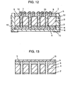
- a photo sensitive resin is applied on the surface of insulation layer 5, as shown in FIG. 13, by using either of the methods among an immersion method, a spin coating process and a screen printing method.
- the photo sensitive resin is cured to form a resist film 15.
- an adhesive organic film may be used for the resist film 15.
- a film is attached on the surface of insulation layer 5. And then, the film is provided with a hole of certain specific dimensions at a location corresponding to the through hole 4, as shown in FIG. 14, by means of a photo processing or a mechanical machining. The film is used as the resist film.
- a solid electrolytic layer 6 and a through hole electrode 7 are provided in the same way as in the embodiment 1, and then the resist film 15 is removed. Thus, no solid electrolytic layer 6 is formed on the other surface, viz. non-porous surface, of aluminum foil 3, and the positive electrode and the negative electrode are surely separated.
- a collector layer 8 is formed on the solid electrolytic layer 6, an opening 9 is formed in the insulation layer 5 disposed on the other surface of aluminum foil 3 at a certain specific location, and a connection terminal 10 is provided at the opening 9 of insulation layer 5 and on the exposed surface of through hole electrode 7, respectively.
- FIG. 15 and FIG. 16 are the drawings used to describe the main process steps of manufacturing an SEC in accordance with a third exemplary embodiment of the present invention.
- an aluminum foil 3 is etched for making it porous, and a dielectric layer 2 is formed on the porous portion. And then, a through hole 4 is formed in aluminum foil 3 at a certain specific location, and an insulation layer 5 is provided to cover the other surface, viz. non-porous surface, of aluminum foil 3 and the inner wall surface of through hole 4.
- a through hole electrode 7 is first formed in the through hole 4, as shown in FIG. 15.
- the through hole electrode 7 is formed by filling a conductive adhesive substance such as Ag paste or Cu paste containing conductive particles, and curing it. And then, a solid electrolytic layer 6 is formed on the dielectric layer 2, as shown in FIG. 16. Therefore, no solid electrolytic layer 6 can be formed on the other surface, viz. non-porous surface, of aluminum foil 3. And then, a collector layer 8 is formed on the solid electrolytic layer 6 in the same way as in the embodiment 1, and an opening 9 is formed in the insulation layer 5 covering the surface of aluminum foil 3 at a certain specific location by means of YAG laser, or the like process.
- a conductive adhesive substance such as Ag paste or Cu paste containing conductive particles
- the opening 9 can be formed instead by providing a resist portion beforehand on the non-porous surface of aluminum foil 3 using photo sensitive resin or the like material prior to formation of the insulation layer 5, and removing the resist portion after collector layer 8 is formed. And then, connection terminal 10 is provided on the exposed surface at the opening 9 and on the through hole electrode 7, respectively.
- FIG. 17 and FIG. 18 are the drawings used to describe the main process steps of manufacturing an SEC in accordance with a fourth exemplary embodiment of the present invention.
- an aluminum foil 3 is etched for making it porous, and a dielectric layer 2 is formed on the porous portion. And then, a first through hole 4 is formed in the aluminum foil 3 at a certain specific location. So far the procedure remains the same as in the embodiment 1.
- an insulation layer 5 is formed to cover the other surface, viz. non-porous surface, of aluminum foil 3 and the inner wall surface of through hole 4.
- a solid electrolytic layer 6 is provided on the dielectric layer 2. If the through hole has a diameter 80 ⁇ m or larger, the solid electrolytic layer 6 could form on the other surface, viz. non-porous surface, of aluminum foil 3.
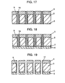
- an insulation layer 5 is formed on the other surface, viz. non-porous surface, of aluminum foil 3, and an insulating portion 16 inside the first through hole, in the first place as shown in FIG. 17.
- the insulation layer 5 is formed in the same way as in the embodiment 1.
- the insulating portion 16 can be provided by electrodepositing an easy-to-fill insulating resin for several times to fill the through hole, or screen-printing or potting an insulating resin. And then, as shown in FIG. 18, a solid electrolytic layer 6 is formed on the dielectric layer. And, as shown in FIG. 19, a second through hole 17 is formed inside the insulating portion 16.
- no solid electrolytic layer 6 can be formed on the other surface, viz. non-porous surface, of aluminum foil 3.
- a through hole electrode 7 is formed in the second through hole 17
- a collector layer 8 is formed on the solid electrolytic layer 6, and then the insulation layer 5 disposed on the aluminum foil 3 is provided with an opening 9 at a certain specific place, and a connection terminal 10 is provided at the opening 9 of insulation layer 5 and on the exposed surface of through hole electrode 7.
- the reliability in insulation between the through hole electrode 7 and the aluminum foil 3 is improved, and a possible spreading of solid electrolytic material onto the aluminum foil 3 at the opening 9 is prevented, to a sure separation between the positive electrode and the negative electrode.
- connection terminals provided at the opening of insulation layer and on the exposed surface of through hole electrode, respectively are disposed on a single flat plane.
Landscapes
- Engineering & Computer Science (AREA)
- Power Engineering (AREA)
- Microelectronics & Electronic Packaging (AREA)
- Fixed Capacitors And Capacitor Manufacturing Machines (AREA)
- Electric Double-Layer Capacitors Or The Like (AREA)
Applications Claiming Priority (3)
| Application Number | Priority Date | Filing Date | Title |
|---|---|---|---|
| JP2001190965 | 2001-06-25 | ||
| JP2001190965A JP4604403B2 (ja) | 2001-06-25 | 2001-06-25 | 固体電解コンデンサの製造方法 |
| PCT/JP2002/006304 WO2003005387A1 (fr) | 2001-06-25 | 2002-06-24 | Procede de production de condensateur electrolytique solide |
Publications (1)
| Publication Number | Publication Date |
|---|---|
| EP1400995A1 true EP1400995A1 (fr) | 2004-03-24 |
Family
ID=19029657
Family Applications (1)
| Application Number | Title | Priority Date | Filing Date |
|---|---|---|---|
| EP02743708A Withdrawn EP1400995A1 (fr) | 2001-06-25 | 2002-06-24 | Procede de production de condensateur electrolytique solide |
Country Status (5)
| Country | Link |
|---|---|
| US (1) | US6855177B2 (fr) |
| EP (1) | EP1400995A1 (fr) |
| JP (1) | JP4604403B2 (fr) |
| CN (1) | CN1465079A (fr) |
| WO (1) | WO2003005387A1 (fr) |
Cited By (1)
| Publication number | Priority date | Publication date | Assignee | Title |
|---|---|---|---|---|
| CN101414511B (zh) * | 2007-10-19 | 2011-10-05 | 吴英宙 | 金属电容器及其制造方法 |
Families Citing this family (13)
| Publication number | Priority date | Publication date | Assignee | Title |
|---|---|---|---|---|
| JP4019837B2 (ja) * | 2002-07-19 | 2007-12-12 | 松下電器産業株式会社 | 固体電解コンデンサ及びその製造方法 |
| CN1998056A (zh) * | 2004-07-15 | 2007-07-11 | 松下电器产业株式会社 | 电容器 |
| JP4738299B2 (ja) * | 2006-09-20 | 2011-08-03 | 富士通株式会社 | キャパシタ、その製造方法、および電子基板 |
| US7608538B2 (en) | 2007-01-05 | 2009-10-27 | International Business Machines Corporation | Formation of vertical devices by electroplating |
| JP4478695B2 (ja) * | 2007-03-19 | 2010-06-09 | ニチコン株式会社 | 固体電解コンデンサ素子およびそれを備えた固体電解コンデンサ |
| US7876548B2 (en) * | 2007-04-20 | 2011-01-25 | Sanyo Electric Co., Ltd. | Niobium solid electrolytic capacitor and its production method |
| US8116062B2 (en) * | 2007-10-19 | 2012-02-14 | Oh Young Joo | Metal capacitor to improve electric conductivity |
| JP4825784B2 (ja) * | 2007-12-13 | 2011-11-30 | 新光電気工業株式会社 | 半導体装置用パッケージおよびその製造方法 |
| US8203823B2 (en) * | 2008-01-11 | 2012-06-19 | Oh Young Joo | Metal capacitor and manufacturing method thereof |
| TWI405322B (zh) | 2010-12-29 | 2013-08-11 | 財團法人工業技術研究院 | 內藏電容基板模組 |
| US9013893B2 (en) | 2010-12-29 | 2015-04-21 | Industrial Technology Research Institute | Embedded capacitor module |
| TWI483352B (zh) | 2012-03-12 | 2015-05-01 | Ind Tech Res Inst | 固態電解電容基板模組及包括該固態電解電容基板模組的電路板 |
| KR20180108807A (ko) | 2016-03-25 | 2018-10-04 | 후지필름 가부시키가이샤 | 알루미늄판의 제조 방법, 및 알루미늄판의 제조 장치 |
Family Cites Families (8)
| Publication number | Priority date | Publication date | Assignee | Title |
|---|---|---|---|---|
| US3864169A (en) * | 1973-02-13 | 1975-02-04 | Nl Industries Inc | A method for making laminated electrodes |
| JPH02137311A (ja) * | 1988-11-18 | 1990-05-25 | Marcon Electron Co Ltd | 固体電解コンデンサ |
| JPH05205984A (ja) | 1992-01-27 | 1993-08-13 | Nec Corp | 積層型固体電解コンデンサ |
| JP3351224B2 (ja) * | 1996-01-31 | 2002-11-25 | 日立エーアイシー株式会社 | 電解コンデンサ |
| JPH11274002A (ja) | 1998-03-25 | 1999-10-08 | Nichicon Corp | チップ型積層固体電解コンデンサ |
| JP3337018B2 (ja) * | 1999-11-19 | 2002-10-21 | 株式会社村田製作所 | 積層コンデンサ、配線基板、デカップリング回路および高周波回路 |
| JP4479050B2 (ja) * | 2000-04-20 | 2010-06-09 | パナソニック株式会社 | 固体電解コンデンサ |
| JP4432207B2 (ja) * | 2000-05-25 | 2010-03-17 | パナソニック株式会社 | コンデンサ |
-
2001
- 2001-06-25 JP JP2001190965A patent/JP4604403B2/ja not_active Expired - Fee Related
-
2002
- 2002-06-24 WO PCT/JP2002/006304 patent/WO2003005387A1/fr not_active Ceased
- 2002-06-24 CN CN02802197A patent/CN1465079A/zh active Pending
- 2002-06-24 EP EP02743708A patent/EP1400995A1/fr not_active Withdrawn
- 2002-06-24 US US10/362,227 patent/US6855177B2/en not_active Expired - Fee Related
Non-Patent Citations (1)
| Title |
|---|
| See references of WO03005387A1 * |
Cited By (1)
| Publication number | Priority date | Publication date | Assignee | Title |
|---|---|---|---|---|
| CN101414511B (zh) * | 2007-10-19 | 2011-10-05 | 吴英宙 | 金属电容器及其制造方法 |
Also Published As
| Publication number | Publication date |
|---|---|
| JP4604403B2 (ja) | 2011-01-05 |
| US20030154583A1 (en) | 2003-08-21 |
| CN1465079A (zh) | 2003-12-31 |
| US6855177B2 (en) | 2005-02-15 |
| JP2003007570A (ja) | 2003-01-10 |
| WO2003005387A9 (fr) | 2005-02-24 |
| WO2003005387A1 (fr) | 2003-01-16 |
Similar Documents
| Publication | Publication Date | Title |
|---|---|---|
| JP4432207B2 (ja) | コンデンサ | |
| JP4479050B2 (ja) | 固体電解コンデンサ | |
| US8652920B2 (en) | Substrate with embedded patterned capacitance | |
| JP4019837B2 (ja) | 固体電解コンデンサ及びその製造方法 | |
| US6775126B2 (en) | Solid electrolytic capacitor and method of manufacturing capacitor | |
| US6855177B2 (en) | Method for producing solid electrolytic capacitor | |
| JP3982496B2 (ja) | 固体電解コンデンサの製造方法 | |
| US6794260B2 (en) | Method of manufacturing solid-state electrolytic capacitor | |
| JP2002299161A (ja) | 複合電子部品 | |
| JP4337423B2 (ja) | 回路モジュール | |
| JP2003068574A (ja) | 固体電解コンデンサの製造方法 | |
| JP2003031438A (ja) | 固体電解コンデンサの製造方法 | |
| JP2003115418A (ja) | 固体電解コンデンサの製造方法 | |
| JP2003017368A (ja) | 固体電解コンデンサの製造方法 | |
| JP2003100564A (ja) | 固体電解コンデンサの製造方法 | |
| JP2002367866A (ja) | 固体電解コンデンサ | |
| JP2003031439A (ja) | 固体電解コンデンサの製造方法 | |
| JP2003007569A (ja) | 固体電解コンデンサの製造方法 |
Legal Events
| Date | Code | Title | Description |
|---|---|---|---|
| PUAI | Public reference made under article 153(3) epc to a published international application that has entered the european phase |
Free format text: ORIGINAL CODE: 0009012 |
|
| 17P | Request for examination filed |
Effective date: 20030221 |
|
| AK | Designated contracting states |
Kind code of ref document: A1 Designated state(s): AT BE CH CY DE DK ES FI FR GB GR IE IT LI LU MC NL PT SE TR |
|
| STAA | Information on the status of an ep patent application or granted ep patent |
Free format text: STATUS: THE APPLICATION HAS BEEN WITHDRAWN |
|
| 18W | Application withdrawn |
Effective date: 20080212 |