EP1401129B1 - Pulsformung für optische duobinäre Signale - Google Patents
Pulsformung für optische duobinäre Signale Download PDFInfo
- Publication number
- EP1401129B1 EP1401129B1 EP03255916A EP03255916A EP1401129B1 EP 1401129 B1 EP1401129 B1 EP 1401129B1 EP 03255916 A EP03255916 A EP 03255916A EP 03255916 A EP03255916 A EP 03255916A EP 1401129 B1 EP1401129 B1 EP 1401129B1
- Authority
- EP
- European Patent Office
- Prior art keywords
- signal
- level signal
- level
- optical
- bits
- Prior art date
- Legal status (The legal status is an assumption and is not a legal conclusion. Google has not performed a legal analysis and makes no representation as to the accuracy of the status listed.)
- Expired - Lifetime
Links
- 230000003287 optical effect Effects 0.000 title claims description 80
- 238000007493 shaping process Methods 0.000 title description 8
- 238000000034 method Methods 0.000 claims description 28
- 238000013507 mapping Methods 0.000 claims description 12
- 230000005540 biological transmission Effects 0.000 claims description 5
- 238000006243 chemical reaction Methods 0.000 claims description 3
- 238000004891 communication Methods 0.000 description 30
- 230000003595 spectral effect Effects 0.000 description 8
- 239000006185 dispersion Substances 0.000 description 6
- 230000006872 improvement Effects 0.000 description 6
- 238000005516 engineering process Methods 0.000 description 5
- 238000010586 diagram Methods 0.000 description 4
- 238000001228 spectrum Methods 0.000 description 4
- 230000008901 benefit Effects 0.000 description 3
- 230000005684 electric field Effects 0.000 description 2
- 239000013307 optical fiber Substances 0.000 description 2
- 230000009467 reduction Effects 0.000 description 2
- 238000012546 transfer Methods 0.000 description 2
- 230000001934 delay Effects 0.000 description 1
- 238000001514 detection method Methods 0.000 description 1
- 239000002360 explosive Substances 0.000 description 1
- 238000012986 modification Methods 0.000 description 1
- 230000004048 modification Effects 0.000 description 1
- 230000008569 process Effects 0.000 description 1
- 238000011160 research Methods 0.000 description 1
- 230000035945 sensitivity Effects 0.000 description 1
Images
Classifications
-
- H—ELECTRICITY
- H04—ELECTRIC COMMUNICATION TECHNIQUE
- H04B—TRANSMISSION
- H04B10/00—Transmission systems employing electromagnetic waves other than radio-waves, e.g. infrared, visible or ultraviolet light, or employing corpuscular radiation, e.g. quantum communication
- H04B10/25—Arrangements specific to fibre transmission
- H04B10/2507—Arrangements specific to fibre transmission for the reduction or elimination of distortion or dispersion
-
- H—ELECTRICITY
- H04—ELECTRIC COMMUNICATION TECHNIQUE
- H04B—TRANSMISSION
- H04B10/00—Transmission systems employing electromagnetic waves other than radio-waves, e.g. infrared, visible or ultraviolet light, or employing corpuscular radiation, e.g. quantum communication
- H04B10/50—Transmitters
- H04B10/516—Details of coding or modulation
- H04B10/5167—Duo-binary; Alternative mark inversion; Phase shaped binary transmission
Definitions
- the present invention relates generally to optical communication systems and, more particularly, to optical communication systems employing duobinary, multilevel pulse-amplitude modulation techniques.
- Duobinary pulse shaping techniques reduce the required signal bandwidth by a factor of two by mapping a binary data signal to a three-level signal.
- duobinary modulation formats employ two signal levels (+1 and -1) to represent a binary value of one, and one signal level (0) to represent a binary value zero.
- the narrow spectral width of duobinary signals compared to a conventional non-return-to-zero (NRZ) binary signal, has been exploited to minimize dispersion sensitivity and to enable dense wavelength division multiplexing techniques. It has been observed that modulating an optical signal with a duobinary electrical signal, as opposed to a standard non-return to zero (NRZ) signal, reduces the optical spectrum by a factor of two,
- United States Patent Lumber 6,424,444 discloses methods and apparatus to transmit and receive information bits encoded in duobinary, multilevel pulse-amplitude-modulated (PAM) optical signals.
- the transmitted optical signal has a narrow optical spectrum and a low symbol rate.
- Information bits are encoded in a M-ary PAM symbol sequence, where M ⁇ 2.
- a subtraction-based encoder precodes and duobinary filters the M-ary PAM symbol sequence, yielding an encoded sequence.
- the encoded sequence is lowpass filtered and modulated onto an optical electric field.
- the receiver processes a received optical electric field to obtain an electrical signal proportional to the received optical intensity, and performs M-ary symbol-by-symbol decisions to recover the transmitted information bits, without potential error propagation.
- improved spectral efficiency will allow greater tolerance to dispersion and the use of generic and available optical technologies.
- a factor of four improvement in spectral efficiency, for example, would provide a 40 Gbps optical communication system using existing 10 Gbps optical communication systems.
- a method for transmitting information according to claim 1 In accordance with the invention there is further provided a method for receiving information according to claim 4.
- the invention further provides a system for transmitting information according to claim 6. Further the invention provides a system for receiving information according to claim 8.
- a duobinary optical communication system employs pulse amplitude modulation (PAM) techniques to provide further improvements in spectral efficiency.
- a disclosed PAM duobinary optical transmitter converts a plurality of input bits to an N level signal using PAM techniques; adds a current N level signal to a previous N level signal to produce a 2N-1 level signal; and converts the 2N-1 level signal to an optical signal for transmission to a receiver.
- the plurality of input bits can be converted to the N level signal by adding a current plurality of input bits to a previous plurality of output bits.
- a disclosed PAM duobinary optical receiver detects a power level of the received optical signal (encoded using pulse amplitude modulation and duobinary encoding techniques to encode a plurality of bits) and maps the detected power level to a plurality of bits to return the transmitted information.
- the detection of the power level of the received optical signal can also convert the optical signal to an electrical signal.
- a squaring operation can be performed to convert the optical signal to an electrical signal. The squaring operation automatically converts the received 2N-1 level signal to an N level signal.
- PAM-4 modulation techniques are combined with duobinary pulse shaping techniques to provide an overall factor of four improvement in spectral efficiency by reducing the bandwidth of the optical signal.
- a 2.5Gbps optical communication system can be upgraded to provide a 10Gbps optical communication system and a 10Gbps optical communication system can be upgraded to provide a 40Gbps optical communication system within the same bandwidth.
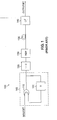
- FIG. 1 is a schematic block diagram of an exemplary conventional duobinary optical communication system 100 that employs three levels to encode each bit.
- the input bit is applied to one terminal of an exclusive or (XOR) gate 110 and the previous bit is applied to the second terminal of the XOR gate 110.
- the previous bit is obtained by a feedback loop containing a delay element 150.
- the XOR gate 110 and delay element 150 comprise a precoder 115 that introduces a correlation into the transmitted signal by adding the previous output bit to the current input bit.
- the precoder 115 is said to perform a 1 / (1+D) ⁇ mod 2 ⁇ operation, where D is a delay operation that delays the sequence of bits by one bit interval.
- the output of the precoder 115 is a two level value (0 or 1) that is applied to an encoder 120 that maps the two level value to a three level value.
- the encoder 120 adds the previous and current bit levels together to produce a three level value (0, 1, 2) according to the following table: Previous Bit Current Bit Three Level Value 1 1 2 1 0 1 0 1 1 0 0 0 0
- the three level value generated by the encoder 120 is applied to a Mach Zehnder modulator 130 that maps each of the three levels (0, 1, 2) to a corresponding voltage level (-V, 0, +V), in a known manner.
- the generated voltage level is then converted to an optical signal (-e, 0, +e) and applied to an optical fiber 135.
- the receiver includes a power detector 140 that decodes the received optical signal.
- the power detector 140 performs an optical to electrical conversion by performing a squaring operation on the received signal. Since the received signal can have one of three optical values (-e, 0, e), the squaring operation returns the signal to +e 2 , or 0. Thereafter, the two levels generated by the power detector 140 are mapped to the corresponding one bit binary value. In this manner, the Mod 2 operation at the receiver is automatically obtained by going through the mapping table and from the optical to electrical domain (-V is equivalent to +V when measuring intensity). Thus, the bit at the output of the duobinary optical communication system 100 is equal to the input bit.
- the duobinary optical communication system 100 provides a factor of two bandwidth reduction of the optical spectrum and thus improves performance in the presence of dispersion.
- a suitable conventional duobinary optical communication system 100 see for example, Kazushige Yonenaga and Shigeru Kuwano, "Dispersion-Tolerant Optical Transmission System Using Duobinary Transmitter and Binary Receiver," J. of Lightwave Technology, Vol. 15, No. 8, 1530-1537 (August, 1997 ).
- duobinary pulse shaping techniques are employed in conjunction with pulse amplitude modulation (PAM) techniques.
- PAM pulse amplitude modulation
- the present invention thus recognizes that the spectral efficiency improvements obtained using duobinary pulse shaping techniques can be further improved by taking advantage of PAM modulation.
- PAM-4 modulation techniques are combined with duobinary pulse shaping techniques to provide an overall factor of four improvement in spectral efficiency by reducing the bandwidth of the optical signal.
- a 2.5Gbps optical communication system can be upgraded to provide a 10Gbps optical communication system and a 10Gbp optical communication system can be upgraded to provide a 40Gbps optical communication system within the same bandwidth.
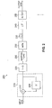
- FIG. 2 is a schematic block diagram of an exemplary PAM-4 duobinary optical communication system 200 incorporating features of the present invention.
- two input bits comprising four levels
- the previous four level value is applied to the second terminal of the adder 210.
- the previous four level value is obtained by a feedback loop containing a delay element 250.
- the adder 210 and delay element 250 comprise a precoder 215 that introduces a correlation into the transmitted signal by adding the previous four level output value to the current four level input value.
- the precoder 215 is said to perform a 1 / (1+D) ⁇ mod 4 ⁇ operation and the output is a four level value.
- the four level output of the precoder 215 is applied to an encoder 220 that maps the four levels to a seven level value (0, 1, 2, 3, 4, 5, 6).
- the encoder 220 adds the previous and current four level values together to produce a seven level value according to the following table: Previous Four Level Value Current Four Level Value Seven Level Value 0 0 0 0 0 1 1 0 2 2 0 3 3 1 0 1 1 1 2 1 2 3 1 3 4 2 0 2 2 1 3 2 2 4 2 3 5 3 0 3 3 1 4 3 2 5 3 3 6
- the seven level value generated by the encoder 220 is applied to a digital to analog converter (DAC) 225 that maps the seven level value to a corresponding voltage.
- DAC digital to analog converter
- the digital to analog converter 225 may employ the following exemplary mapping: 0 1 2 3 6 5 4 ⁇ - 3 ⁇ V , - 2 ⁇ V , - V , 0 , V , 2 ⁇ V , 3 ⁇ V , respectively. It is noted that other mappings by the digital to analog converter 225 are possible.
- a Mach Zehnder modulator 230 then maps each of the seven voltage levels (-3V, -2V, -V, 0, V, 2V, 3V) to a corresponding optical signal (-3e, -2e, -e, 0, e, 2e, 3e) and the optical signal is applied to an optical fiber 235.
- the receiver includes a power detector 240 that decodes the received optical signal.
- the power detector 240 performs an optical to electrical conversion by performing a squaring operation on the received signal. Since the received signal can have one of seven optical values (-3e, -2e, -e, 0, e, 2e, 3e), the squaring operation returns the signal to +9e 2 , +4e 2 , +e 2 , or 0.
- a slicer 260 maps the four levels generated by the power detector 240 to the corresponding two bit binary value. In this manner, the Mod 4 operation at the receiver is automatically obtained by going through the mapping table of the slicer 260 and from the optical to electrical domain (-V is equivalent to +V when measuring intensity).
- the two bits at the output of the PAM-4 duobinary optical communication system 200 are equal to the input bits.
- the PAM-4 duobinary optical communication system 200 provides a factor of four bandwidth reduction of the optical spectrum and thus improves performance in the presence of dispersion.
Landscapes
- Physics & Mathematics (AREA)
- Electromagnetism (AREA)
- Engineering & Computer Science (AREA)
- Computer Networks & Wireless Communication (AREA)
- Signal Processing (AREA)
- Optical Communication System (AREA)
Claims (10)
- Verfahren zum Senden von Informationen, wobei das Verfahren die folgenden Schritte umfasst:Umsetzen mehrerer Eingangsbits in ein N-Pegel-Signal;Addieren (210) eines momentanen N-Pegel-Signals zu einem vorhergehenden N-Pegel-Signal, um ein (2N - 1)-Pegel-Signal zu erzeugen, wobei das (2N - 1)-Pegel-Signal auf eine entsprechende (2N - 1)-Pegel-Signalspannung abgebildet wird, die eine umgeordnete Gruppe von 2N - 1 Pegeln besitzt, und wobei das Abbilden eine Quadrierungsoperation bei einem Empfänger ermöglicht, um zu veranlassen, dass ein empfangenes Signal als eine Modulo-N-Operation erscheint; undAusführen einer Analog/Digital-Umsetzung (220, 225, 230) des (2N - 1)-Pegel-Signals in ein optisches Signal, um es zu dem Empfänger zu senden.
- Verfahren nach Anspruch 1, wobei der Schritt des Umsetzens mehrerer Eingangsbits in ein N-Pegel-Signal ferner den Schritt des Addierens einer momentanen Mehrzahl von Eingangsbits zu einer vorhergehenden Mehrzahl von Ausgangsbits umfasst, um das N-Pegel-Signal zu erzeugen.
- Verfahren nach Anspruch 1, wobei der Additionsschritt ferner den Schritt des Abbildens eines 7-Pegel-Werts auf einen entsprechenden Spannungswert in der folgenden Weise umfasst:(0, 1, 2, 3, 6, 5, 4) → (-3 V, -2 V, -V, 0, V, 2 V, 3 V) entsprechend.
- Verfahren zum Empfangen von Informationen, wobei das Verfahren die folgenden Schritte umfasst:Empfangen eines optischen Signals, wobei das optische Signal gemäß Anspruch 1 unter Verwendung einer Impuls-Amplituden-Modulation und von duo-binären Codierungstechniken codiert wird, um mehrere Bits zu codieren;Detektieren eines Leistungspegels des empfangenen optischen Signals; undAbbilden des detektierten Leistungspegels auf mehrere Bits, wobei ein (2N - 1)-Pegel-Signal auf eine entsprechende (2N - 1)-Pegel-Signalspannung, die eine umgeordnete Gruppe von 2N - 1 Pegeln besitzt, abgebildet wird, wobei die Abbildung eine Quadrierungsoperation ermöglicht, um zu bewirken, dass das empfangene Signal als eine Modulo-N-Operation erscheint.
- Verfahren nach Anspruch 4, wobei der Schritt des Umsetzens des optischen Signals in ein elektrisches Signal eine Quadrierungsoperation an dem optischen Signal ausführt.
- System zum Senden von Informationen, wobei das System umfasst:einen Vorcodierer, um mehrere Eingangsbits in ein N-Pegel-Signal umzusetzen;einen Addierer, um ein momentanes N-Pegel-Signal zu einem vorhergehenden N-Pegel-Signal zu addieren, um ein (2N - 1)-Pegel-Signal zu erzeugen, wobei das (2N - 1)-Pegel-Signal auf eine entsprechende (2N - 1)-Pegel-Signalspannung abgebildet wird, die eine umgeordnete Gruppe von 2N - 1 Pegeln besitzt, und wobei die Abbildung in der Weise konfiguriert ist, dass eine Quadrierungsoperation bei einem Empfänger dazu ausgelegt ist, ein empfangenes Signal als eine Modulo-N-Operation erscheinen zu lassen; undeinen Digital/Analog-Umsetzer, um das (2N - 1)-Pegel-Signal in ein optisches Signal umzusetzen, um es zu dem Empfänger zu senden.
- System nach Anspruch 6, wobei der Vorcodierer einen Addierer umfasst, um eine momentane Mehrzahl von Eingangsbits zu einer vorhergehenden Mehrzahl von Ausgangsbits zu addieren, um das N-Pegel-Signal zu erzeugen.
- System zum Empfangen von Informationen, wobei das System umfasst:einen Eingangsanschluss, um ein optisches Signal zu empfangen, wobei das optische Signal gemäß Anspruch 1 unter Verwendung einer Impuls-Amplituden-Modulation und von duo-binären Codierungstechniken codiert wird, um mehrere Bits zu codieren;einen Leistungsdetektor, um einen Leistungspegel des empfangenen optischen Signals zu detektieren; undeinen Slicer, um den detektierten Leistungspegel auf mehrere Bits abzubilden, wobei ein (2N - 1)-Pegel-Signal auf eine entsprechende (2N - 1)-Pegel-Signalspannung abgebildet wird, die eine umgeordnete Gruppe von 2N - 1 Pegeln besitzt, wobei die Abbildung in der Weise konfiguriert ist, dass eine Quadrierungsoperation dazu ausgelegt ist, dass das empfangene Signal als eine Modulo-N-Operation erscheint.
- System nach Anspruch 8, wobei der Leistungsdetektor dazu ausgelegt ist, das optische Signal in ein elektrisches Signal umzusetzen.
- System nach Anspruch 9, wobei die optisch-elektrische Umsetzung dazu ausgelegt ist, eine Quadrierungsoperation an dem optischen Signal auszuführen.
Applications Claiming Priority (4)
| Application Number | Priority Date | Filing Date | Title |
|---|---|---|---|
| US378096 | 1999-08-20 | ||
| US41287002P | 2002-09-23 | 2002-09-23 | |
| US412870P | 2002-09-23 | ||
| US10/378,096 US7257329B2 (en) | 2002-09-23 | 2003-02-28 | Duobinary pulse shaping for optical transmission systems employing pulse amplitude modulation techniques |
Publications (3)
| Publication Number | Publication Date |
|---|---|
| EP1401129A2 EP1401129A2 (de) | 2004-03-24 |
| EP1401129A3 EP1401129A3 (de) | 2006-04-26 |
| EP1401129B1 true EP1401129B1 (de) | 2009-11-25 |
Family
ID=31949840
Family Applications (1)
| Application Number | Title | Priority Date | Filing Date |
|---|---|---|---|
| EP03255916A Expired - Lifetime EP1401129B1 (de) | 2002-09-23 | 2003-09-22 | Pulsformung für optische duobinäre Signale |
Country Status (3)
| Country | Link |
|---|---|
| US (1) | US7257329B2 (de) |
| EP (1) | EP1401129B1 (de) |
| DE (1) | DE60330212D1 (de) |
Families Citing this family (26)
| Publication number | Priority date | Publication date | Assignee | Title |
|---|---|---|---|---|
| ATE407485T1 (de) * | 2005-04-04 | 2008-09-15 | Alcatel Lucent | Betriebsverfahren für ein passives optisches netzwerk |
| US7574145B2 (en) * | 2005-12-30 | 2009-08-11 | Intel Corporation | Optical receiver with duo-binary encoder |
| US7483597B2 (en) * | 2006-10-19 | 2009-01-27 | Lightwire, Inc. | Optical modulator utilizing multi-level signaling |
| WO2015172375A1 (zh) * | 2014-05-16 | 2015-11-19 | 华为技术有限公司 | 一种通信方法、装置及系统 |
| US10078232B1 (en) * | 2014-07-11 | 2018-09-18 | Acacia Communications, Inc. | Advanced optical modulation generation by combining orthogonal polarized optical signals |
| KR102036539B1 (ko) * | 2016-07-20 | 2019-10-28 | 전자부품연구원 | 고효율 광신호 전송을 위한 펄스진폭변조 기반 광송신기 |
| US10938485B2 (en) | 2019-04-18 | 2021-03-02 | Microsoft Technology Licensing, Llc | Error control coding with dynamic ranges |
| US11018776B2 (en) | 2019-04-18 | 2021-05-25 | Microsoft Technology Licensing, Llc | Power-based decoding of data received over an optical communication path |
| US10873393B2 (en) | 2019-04-18 | 2020-12-22 | Microsoft Technology Licensing, Llc | Receiver training for throughput increases in optical communications |
| US10897315B2 (en) | 2019-04-18 | 2021-01-19 | Microsoft Technology Licensing, Llc | Power-based decoding of data received over an optical communication path |
| US10892847B2 (en) | 2019-04-18 | 2021-01-12 | Microsoft Technology Licensing, Llc | Blind detection model optimization |
| US10873392B2 (en) | 2019-04-18 | 2020-12-22 | Microsoft Technology Licensing, Llc | Throughput increases for optical communications |
| US10742325B1 (en) * | 2019-04-18 | 2020-08-11 | Microsoft Technology Licensing, Llc | Power-based encoding of data to be transmitted over an optical communication path |
| US10911155B2 (en) | 2019-04-18 | 2021-02-02 | Microsoft Technology Licensing, Llc | System for throughput increases for optical communications |
| US10998982B2 (en) | 2019-04-18 | 2021-05-04 | Microsoft Technology Licensing, Llc | Transmitter for throughput increases for optical communications |
| US10911152B2 (en) | 2019-04-18 | 2021-02-02 | Microsoft Technology Licensing, Llc | Power-based decoding of data received over an optical communication path |
| US10756817B1 (en) | 2019-04-18 | 2020-08-25 | Microsoft Technology Licensing, Llc | Power switching for systems implementing throughput improvements for optical communications |
| US10862591B1 (en) | 2019-04-18 | 2020-12-08 | Microsoft Technology Licensing, Llc | Unequal decision regions for throughput increases for optical communications |
| US10951342B2 (en) | 2019-04-18 | 2021-03-16 | Microsoft Technology Licensing, Llc | Throughput increases for optical communications |
| US10742326B1 (en) | 2019-04-18 | 2020-08-11 | Microsoft Technology Licensing, Llc | Power-based encoding of data to be transmitted over an optical communication path |
| US10686530B1 (en) | 2019-04-18 | 2020-06-16 | Microsoft Technology Licensing, Llc | Power-based encoding of data to be transmitted over an optical communication path |
| US10911141B1 (en) | 2019-07-30 | 2021-02-02 | Microsoft Technology Licensing, Llc | Dynamically selecting a channel model for optical communications |
| CN111478733B (zh) * | 2020-03-29 | 2023-06-27 | 复旦大学 | 基于双极化光强度调制器的pam4电信号产生系统 |
| CN112054977B (zh) * | 2020-09-16 | 2022-05-27 | 湖南工商大学 | 一种基于功率谱整形的光传输方法及装置 |
| CN112511236B (zh) * | 2020-11-17 | 2022-03-25 | 北京邮电大学 | 一种pam-4单波长传输方法和装置 |
| US12401553B2 (en) | 2022-09-28 | 2025-08-26 | Samsung Electronics, Co., Ltd. | Semiconductor device |
Family Cites Families (3)
| Publication number | Priority date | Publication date | Assignee | Title |
|---|---|---|---|---|
| FR1559633A (de) * | 1967-10-12 | 1969-03-14 | ||
| US6424444B1 (en) * | 2001-01-29 | 2002-07-23 | Stratalight Communications, Inc. | Transmission and reception of duobinary multilevel pulse-amplitude-modulated optical signals using finite-state machine-based encoder |
| US6490069B1 (en) * | 2001-01-29 | 2002-12-03 | Stratalight Communications, Inc. | Transmission and reception of duobinary multilevel pulse-amplitude-modulated optical signals using subtraction-based encoder |
-
2003
- 2003-02-28 US US10/378,096 patent/US7257329B2/en not_active Expired - Fee Related
- 2003-09-22 DE DE60330212T patent/DE60330212D1/de not_active Expired - Lifetime
- 2003-09-22 EP EP03255916A patent/EP1401129B1/de not_active Expired - Lifetime
Also Published As
| Publication number | Publication date |
|---|---|
| DE60330212D1 (de) | 2010-01-07 |
| EP1401129A2 (de) | 2004-03-24 |
| EP1401129A3 (de) | 2006-04-26 |
| US20040057733A1 (en) | 2004-03-25 |
| US7257329B2 (en) | 2007-08-14 |
Similar Documents
| Publication | Publication Date | Title |
|---|---|---|
| US7257329B2 (en) | Duobinary pulse shaping for optical transmission systems employing pulse amplitude modulation techniques | |
| US7149256B2 (en) | Multilevel pulse position modulation for efficient fiber optic communication | |
| US4763326A (en) | Service-integrating, digital message transmission system for joint transmission of narrow-band and broadband signals | |
| US7515832B2 (en) | Optical transmission equipment and integrated circuit | |
| CA2295390C (en) | Methods of and apparatus for optical signal transmission | |
| US7983570B2 (en) | Direct detection differential polarization-phase-shift keying for high spectral efficiency optical communication | |
| US7155134B2 (en) | Pulse amplitude modulated transmission scheme for optical channels with soft decision decoding | |
| EP1379042B1 (de) | Multiplexer | |
| EP2830239B1 (de) | Verfahren, System und Sender-Empfängervorrichtung zum bidirektionalen Übertragen digitaler optischer Signale über einen optischen Übertragungslink | |
| US4677608A (en) | Method of transferring an additional information channel across a transmission medium | |
| EP2843854B1 (de) | Verfahren, Sender- und Empfängervorrichtung zur Übertragung eines binären digitalen Sendesignals über eine optische Übertragungsstrecke | |
| WO2000051354A1 (en) | Digital optical transmitter for processing externally generated information in a catv reverse path | |
| CA2446765A1 (en) | High-speed adjustable multilevel light modulation | |
| US20100316389A1 (en) | Method for non-flutter transmission of digital data in a free-space optical transmission system | |
| US8577224B2 (en) | Optical shaping for amplification in a semiconductor optical amplifier | |
| US20030180055A1 (en) | Optically calibrated pulse amplitude modulated transmission scheme for optical channels | |
| JP3371857B2 (ja) | 光伝送装置 | |
| US6304353B1 (en) | System and method for improved signal to noise ratio in optical communications networks | |
| EP3497825B1 (de) | Codierung für optische übertragung | |
| US6404819B1 (en) | System and method for generating NRZ signals from RZ signals in communications networks | |
| JP4351508B2 (ja) | パルス振幅変調技法を使用する光伝送システム用のデュオバイナリ・パルス整形 | |
| US20030223761A1 (en) | Embedded operational channel network management | |
| US10122465B2 (en) | Digital signal processing device and optical transceiver apparatus | |
| US6580538B1 (en) | Reduction of optical impairments in wavelength division multiplexed systems employing a wavelength bus architecture | |
| US6542276B1 (en) | Method and apparatus for increasing the spectral efficiency of dense wavelength division multiplexed systems |
Legal Events
| Date | Code | Title | Description |
|---|---|---|---|
| PUAI | Public reference made under article 153(3) epc to a published international application that has entered the european phase |
Free format text: ORIGINAL CODE: 0009012 |
|
| AK | Designated contracting states |
Kind code of ref document: A2 Designated state(s): AT BE BG CH CY CZ DE DK EE ES FI FR GB GR HU IE IT LI LU MC NL PT RO SE SI SK TR |
|
| AX | Request for extension of the european patent |
Extension state: AL LT LV MK |
|
| PUAL | Search report despatched |
Free format text: ORIGINAL CODE: 0009013 |
|
| AK | Designated contracting states |
Kind code of ref document: A3 Designated state(s): AT BE BG CH CY CZ DE DK EE ES FI FR GB GR HU IE IT LI LU MC NL PT RO SE SI SK TR |
|
| AX | Request for extension of the european patent |
Extension state: AL LT LV MK |
|
| RIC1 | Information provided on ipc code assigned before grant |
Ipc: H04B 10/18 20060101AFI20031218BHEP Ipc: H04B 10/158 20060101ALI20060307BHEP |
|
| 17P | Request for examination filed |
Effective date: 20060629 |
|
| AKX | Designation fees paid |
Designated state(s): DE FR GB |
|
| 17Q | First examination report despatched |
Effective date: 20070202 |
|
| GRAP | Despatch of communication of intention to grant a patent |
Free format text: ORIGINAL CODE: EPIDOSNIGR1 |
|
| RAP1 | Party data changed (applicant data changed or rights of an application transferred) |
Owner name: AGERE SYSTEMS INC. |
|
| GRAS | Grant fee paid |
Free format text: ORIGINAL CODE: EPIDOSNIGR3 |
|
| GRAA | (expected) grant |
Free format text: ORIGINAL CODE: 0009210 |
|
| AK | Designated contracting states |
Kind code of ref document: B1 Designated state(s): DE FR GB |
|
| REG | Reference to a national code |
Ref country code: GB Ref legal event code: FG4D |
|
| REF | Corresponds to: |
Ref document number: 60330212 Country of ref document: DE Date of ref document: 20100107 Kind code of ref document: P |
|
| PLBE | No opposition filed within time limit |
Free format text: ORIGINAL CODE: 0009261 |
|
| STAA | Information on the status of an ep patent application or granted ep patent |
Free format text: STATUS: NO OPPOSITION FILED WITHIN TIME LIMIT |
|
| 26N | No opposition filed |
Effective date: 20100826 |
|
| PGFP | Annual fee paid to national office [announced via postgrant information from national office to epo] |
Ref country code: FR Payment date: 20130910 Year of fee payment: 11 |
|
| REG | Reference to a national code |
Ref country code: DE Ref legal event code: R082 Ref document number: 60330212 Country of ref document: DE Representative=s name: DILG HAEUSLER SCHINDELMANN PATENTANWALTSGESELL, DE |
|
| REG | Reference to a national code |
Ref country code: FR Ref legal event code: ST Effective date: 20150529 |
|
| REG | Reference to a national code |
Ref country code: DE Ref legal event code: R081 Ref document number: 60330212 Country of ref document: DE Owner name: INTEL CORPORATION (N.D.GES.D. STAATES DELAWARE, US Free format text: FORMER OWNER: AGERE SYSTEMS, INC., ALLENTOWN, PA., US Ref country code: DE Ref legal event code: R082 Ref document number: 60330212 Country of ref document: DE Representative=s name: DILG HAEUSLER SCHINDELMANN PATENTANWALTSGESELL, DE Ref country code: DE Ref legal event code: R081 Ref document number: 60330212 Country of ref document: DE Owner name: LSI CORPORATION, SAN JOSE, US Free format text: FORMER OWNER: AGERE SYSTEMS, INC., ALLENTOWN, PA., US |
|
| REG | Reference to a national code |
Ref country code: DE Ref legal event code: R081 Ref document number: 60330212 Country of ref document: DE Owner name: INTEL CORPORATION (N.D.GES.D. STAATES DELAWARE, US Free format text: FORMER OWNER: AGERE SYSTEMS LLC, WILMINGTON, DEL., US Ref country code: DE Ref legal event code: R082 Ref document number: 60330212 Country of ref document: DE Representative=s name: DILG HAEUSLER SCHINDELMANN PATENTANWALTSGESELL, DE Ref country code: DE Ref legal event code: R081 Ref document number: 60330212 Country of ref document: DE Owner name: LSI CORPORATION, SAN JOSE, US Free format text: FORMER OWNER: AGERE SYSTEMS LLC, WILMINGTON, DEL., US |
|
| PG25 | Lapsed in a contracting state [announced via postgrant information from national office to epo] |
Ref country code: FR Free format text: LAPSE BECAUSE OF NON-PAYMENT OF DUE FEES Effective date: 20140930 |
|
| REG | Reference to a national code |
Ref country code: GB Ref legal event code: 732E Free format text: REGISTERED BETWEEN 20161103 AND 20161109 |
|
| REG | Reference to a national code |
Ref country code: DE Ref legal event code: R082 Ref document number: 60330212 Country of ref document: DE Representative=s name: DILG, HAEUSLER, SCHINDELMANN PATENTANWALTSGESE, DE Ref country code: DE Ref legal event code: R082 Ref document number: 60330212 Country of ref document: DE Representative=s name: DILG HAEUSLER SCHINDELMANN PATENTANWALTSGESELL, DE Ref country code: DE Ref legal event code: R081 Ref document number: 60330212 Country of ref document: DE Owner name: INTEL CORPORATION (N.D.GES.D. STAATES DELAWARE, US Free format text: FORMER OWNER: LSI CORPORATION, SAN JOSE, CALIF., US |
|
| REG | Reference to a national code |
Ref country code: GB Ref legal event code: 732E Free format text: REGISTERED BETWEEN 20170202 AND 20170208 |
|
| PGFP | Annual fee paid to national office [announced via postgrant information from national office to epo] |
Ref country code: DE Payment date: 20190910 Year of fee payment: 17 |
|
| PGFP | Annual fee paid to national office [announced via postgrant information from national office to epo] |
Ref country code: GB Payment date: 20190920 Year of fee payment: 17 |
|
| REG | Reference to a national code |
Ref country code: DE Ref legal event code: R119 Ref document number: 60330212 Country of ref document: DE |
|
| GBPC | Gb: european patent ceased through non-payment of renewal fee |
Effective date: 20200922 |
|
| PG25 | Lapsed in a contracting state [announced via postgrant information from national office to epo] |
Ref country code: DE Free format text: LAPSE BECAUSE OF NON-PAYMENT OF DUE FEES Effective date: 20210401 |
|
| PG25 | Lapsed in a contracting state [announced via postgrant information from national office to epo] |
Ref country code: GB Free format text: LAPSE BECAUSE OF NON-PAYMENT OF DUE FEES Effective date: 20200922 |