EP1401166A1 - Verfahren und Vorrichtung zur Übertragung von Sprach- und Musikdaten mittels RZ-Signalen - Google Patents
Verfahren und Vorrichtung zur Übertragung von Sprach- und Musikdaten mittels RZ-Signalen Download PDFInfo
- Publication number
- EP1401166A1 EP1401166A1 EP03103409A EP03103409A EP1401166A1 EP 1401166 A1 EP1401166 A1 EP 1401166A1 EP 03103409 A EP03103409 A EP 03103409A EP 03103409 A EP03103409 A EP 03103409A EP 1401166 A1 EP1401166 A1 EP 1401166A1
- Authority
- EP
- European Patent Office
- Prior art keywords
- signals
- return
- zero
- section
- end terminal
- Prior art date
- Legal status (The legal status is an assumption and is not a legal conclusion. Google has not performed a legal analysis and makes no representation as to the accuracy of the status listed.)
- Withdrawn
Links
Images







Classifications
-
- H—ELECTRICITY
- H04—ELECTRIC COMMUNICATION TECHNIQUE
- H04B—TRANSMISSION
- H04B10/00—Transmission systems employing electromagnetic waves other than radio-waves, e.g. infrared, visible or ultraviolet light, or employing corpuscular radiation, e.g. quantum communication
- H04B10/11—Arrangements specific to free-space transmission, i.e. transmission through air or vacuum
- H04B10/114—Indoor or close-range type systems
- H04B10/1141—One-way transmission
-
- H—ELECTRICITY
- H04—ELECTRIC COMMUNICATION TECHNIQUE
- H04L—TRANSMISSION OF DIGITAL INFORMATION, e.g. TELEGRAPHIC COMMUNICATION
- H04L25/00—Baseband systems
- H04L25/38—Synchronous or start-stop systems, e.g. for Baudot code
- H04L25/40—Transmitting circuits; Receiving circuits
- H04L25/49—Transmitting circuits; Receiving circuits using code conversion at the transmitter; using predistortion; using insertion of idle bits for obtaining a desired frequency spectrum; using three or more amplitude levels ; Baseband coding techniques specific to data transmission systems
- H04L25/4906—Transmitting circuits; Receiving circuits using code conversion at the transmitter; using predistortion; using insertion of idle bits for obtaining a desired frequency spectrum; using three or more amplitude levels ; Baseband coding techniques specific to data transmission systems using binary codes
Definitions
- the present invention relates to a small sized communication apparatus that can be fitted at all times on a body without any discomfort and that transmits and receives analog data such as voice signals.
- the present invention relates to the lowering of power consumption of a system that converts musical sounds such as voice and music into digital signals and then transmits them by infrared rays and the like, and also to the raising of the quality of the transmission of voice by this system.
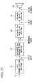
- a device such as that shown in FIG. 23 has been necessary. Namely, in this conventional device a structure is employed in which digital data is transmitted via a 1-bit communication vehicle 17 using an A/D conversion section 81, a parallel - serial conversion section 82, a synchronous data appending section 83, and a 1-bit transmitting section 93. Received digital data is output as voice or music using a 1-bit receiving section 94, a clock recovery section 84, a serial - parallel conversion section 85, a D/A conversion section 86, a speaker drive section 15, and (in the case of voice signals) a speaker 16.
- the A/D conversion section 81 samples input analog voice signals (the voice signals 11) at fixed time intervals, and outputs the voltage value of one interval as an approximately 16-bit (described below as being 16-bit) binary code.
- the parallel - serial conversion section 82 converts 16-bit parallel binary code output from the A/D conversion section 81 into a 16-bit serial data stream. If the A/D conversion section 81 itself outputs binary code in a serial 1-bit data stream, the parallel - serial conversion section 82 is not needed.
- FIG. 24 an example of a 16-bit serial data stream is shown in FIG. 24.
- delimiters namely, synchronization signals
- synchronous data appending section 83 simple examples of this appending of synchronous data include a method in which two bits indicating a start position are appended to the front of D15, while one bit indicating a stop position is appended to the back of D0.
- Another method is one in which several items of data are grouped together to form a frame, and data indicating the frame position is appended to the front of the frame as a frame synchronization signal.
- Various modulations such as frequency shift keying (FSK) and on-off-keying are performed sequentially by the 1-bit transmitting section 93 on serial data streams to which this synchronous data has been appended, and they are emitted via a medium such as electromagnetic waves onto a transmission path, namely, into space which serves as the 1-bit communication vehicle 17.
- FSK frequency shift keying
- on-off-keying are performed sequentially by the 1-bit transmitting section 93 on serial data streams to which this synchronous data has been appended, and they are emitted via a medium such as electromagnetic waves onto a transmission path, namely, into space which serves as the 1-bit communication vehicle 17.
- the electromagnetic waves or the like that are emitted into space are received by the 1-bit receiving section 94 and the received signals are demodulated using the same demodulation format that was used by the transmitting side.
- the same serial data stream is obtained that was output from the synchronous data appending section 83 on the transmitting side.
- start position indication bits and a stop position indication bit contained in this serial data stream are recognized by the clock recovery section 84, and the data D15 to D0 between these position indication bits is output as the data of single group.
- the data of this single group is restored to being 16-bit parallel binary data by the serial - parallel conversion section 85, and this data is then converted into analog signals by the D/A conversion section 86.
- these analog signals are voice signals, for example, they are input into the speaker drive section 15 formed by speaker drive amplifier or the like, and the speaker 16 is driven by the speaker drive section 15 so that sound is obtained.
- voice signals for example, they are input into the speaker drive section 15 formed by speaker drive amplifier or the like, and the speaker 16 is driven by the speaker drive section 15 so that sound is obtained.
- circuits or hardware to realize each of these sections has already been announced publicly or is already in common use.
- a conventional communication device for analog data such as voice signals that uses a digital format has the structure shown in FIG. 23 and, consequently, has the following two problems.
- the first problem is that the size of the circuitry on the receiving side is large. In order to detect synchronous bits it is necessary to perform data processing such as synchronous pattern matching operations and the like. Moreover, in order to correctly receive data it is necessary to create clocks on the receiving side that are synchronized with clocks on the transmitting side from the data received using a synchronous circuit such as a phase locked loop (PLL). Because of this, a timing synchronous circuit such as a PLL circuit or a synchronous signal pattern matching circuit becomes necessary. Furthermore, because the D/A converter is needed to convert binary data into analog signals, the circuit size on the receiving side is enlarged and the power consumption thereof increases.
- PLL phase locked loop
- the second problem is that accurate clock recovery and synchronization timing extraction are necessary.
- the clocks on the transmitting side must be perfectly synchronous with the clocks on the receiving side. If these clocks are even slightly mismatched, then, at some point, data duplications or omissions such as sampling duplication or data skipping are generated, causing data errors to occur. Even if the clocks are perfectly synchronized, if there is an error in the recognition of the synchronous pattern, then the data of a single group is received from partway through that group, which is also a data error.
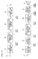
- FIG. 25 shows the structure of the data communication systems disclosed in these publications. Such systems are formed by a 1-bit quantization section 12 that performs noise shaping on input voice signals 11, an infrared ray transmitting section 13, an infrared ray receiving section 14, a speaker drive section 15, and a speaker 16.
- the 1-bit quantization section 12 is formed by a noise shaping A/D converter 21;
- the infrared ray transmitting section 13 is formed by an infrared ray light emitting diode (LED) 23 and an LED driver 22;
- the infrared ray receiving section 14 is formed by a photo-diode 24, a voltage comparator 25, and a comparison level generating circuit 26;
- the speaker drive section 15 is formed by a low pass filter 27 and a power amplifier (drive AMP) 28.
- the LED driver 22 performs on-off-keying by infrared rays which involves the LED driver 22 causing the infrared ray LED 23 to emit light when an output from the noise shaping A/D converter 21 is "1", and causing the infrared ray LED 23 to not emit light when an output from the noise shaping A/D converter 21 is "0".
- the infrared ray LED 23 emits light for light emission timing where the data is "1", and does not emit light for light emission timing where the data is "0".
- FIG. 27A the infrared ray LED 23 emits light for light emission timing where the data is "1", and does not emit light for light emission timing where the data is "0".
- the output voltage of the photo-diode 24 of the infrared ray receiving section 14 swings at a large amplitude when the transmitting section and the receiving section are close to each other and a large quantity of light is received by the receiving section, and, as is shown in FIG. 27C, swings at a small amplitude when the transmitting section and the receiving section are far from each other and a small quantity of light is received by the receiving section.
- This reference voltage Vref is an average voltage of the output voltages of the photo-diode 24 that is generated in the comparison level generating circuit 26.
- Manchester code In the field of communications, however, Manchester code is used to solve the above described problem. As is shown in FIGS. 29A and 29B, in Manchester code, for a logical value "1" light is caused to be emitted from a light emitting diode as a high level signal is input for the timing of the first half of the emission, while, for the timing of the second half of the emission, light is not emitted from the light emitting diode with a low level signal being input.
- the reference voltage Vref Vdd/2 and the aforementioned jitter is not generated.
- voice transmission that uses code converted using noise shaping is based on a process in which, on the receiving side, a high level signal is obtained for "1" and a low level signal is obtained for a "0", and filter processing is performed on the signals thus obtained so as to provide a voice signal. Therefore, the waveform shown in FIG. 29C ends up being received as a result of the voice transmission so that it is not possible to reproduce the original voice. Namely, because the signals shown in FIG. 29C end up as direct current signals even if they are passed through a low pass filter, the voice cannot be reproduced. Therefore, it is necessary to convert them into the signals described above (see FIG. 28C) by performing a decoding process at the receiving side using a decoder.
- the conventional technology that performs transmission by the on-off keying of voice using noise shaping has the drawback that the transmission quality is deteriorated due to jitter being generated in the waveforms of received signals.
- a technology such as Manchester coding, which suppresses jitter that is generated when the same code occurs continuously, is used together with the above technology, as is used in wireless communication and the like, the drawbacks arise that a decoder is required on the receiving side, and the size of the circuitry on the receiving side increases as does the amount of power consumed.
- the present invention was conceived in view of the above drawbacks and it is an object thereof to provide a data communication method, a data transmitting apparatus, data receiving apparatus, and a data transmission program that provide a solution to the problem of jitter that is generated by a combination of a conventional 1-bit noise shaping A/D converter with on-off-keying using infrared rays, without bringing about any increase in the size of the circuitry or in power consumption on the receiving side.
- the data communication method of the present invention is one in which, on a transmitting side, converting analog signals comprising voice or music or digital signals obtained by digitizing voice or music into non-return-to-zero digital signals formed by 1-bit data streams using a noise shaping method; on the transmitting side, using a high level for converted digital signals of "1" and using a low level for converted digital signals of "0", and when a high level is used the converted digital signals are converted into return-to-zero signals having a pulse width smaller than the pulse width of non-return-to-zero signals and then the return-to-zero signals are output, and when a low level is used the converted digital signals are output as they are at a low level; on the transmitting side, transmitting the output signals as radio signals; and on a receiving side, receiving the radio signals from the transmitting side; and on the receiving side, driving a musical sound output section by electrical signals obtained from the received signals so as to convert the electrical signals into musical sound signals.
- the data transmission apparatus of the present invention comprises: a 1-bit conversion section that converts analog signals comprising voice or music or digital signals obtained by digitizing voice or music into non-return-to-zero digital signals formed by 1-bit data streams using a noise shaping method; a return-to-zero section that uses a high level for converted digital signals of "1" and a low level for converted digital signals of "0", and for a high level converts the converted digital signals into return-to-zero signals having a pulse width smaller than the pulse width of non-return-to-zero signals and then outputs the return-to-zero signals, and for a low level outputs the converted digital signals as they are at a low level, and a radio transmitting section that outputs the return-to-zero digital signals as radio signals.
- the data receiving apparatus of the present invention comprises: a radio receiving section that receives by radio return-to-zero digital signals obtained by converting analog signals comprising voice or music or digital signals obtained by digitizing voice or music into digital signals formed by 1-bit data streams, and in which for a logic value of "0" a low level is allocated, while for a logic value of "1" a high level having a pulse width smaller than the pulse width of non-return-to-zero signals is allocated; a musical sound output section that converts electrical signals into musical sound signals; and a drive section that generates return-to-zero drive signals as the electrical signals to drive the musical sound output section based on the return-to-zero digital signals received by the radio receiving section.
- the radio transmitting section may be an infrared ray transmitting section that transmits the return-to-zero digital signals in accordance with the physical layers of Fast IrDA Physical Layer (FIR), which is a digital infrared ray communication standard.
- FIR Fast IrDA Physical Layer
- the radio receiving section may be an infrared ray receiving section that receives by radio the return-to-zero digital signals in accordance with physical the layers of FIR.
- the return-to-zero section may make the pulse width of the return-to-zero digital signals for the high level between 5% or more and less than 40% of the pulse width of non-return-to-zero signals. As a result, an even better noise suppression effect can be obtained.
- a pulse width extension section that extends pulse widths of high level drive signals that have a pulse width of less than 100% of the pulse width of high level non-return-to-zero signals to a pulse width of 100% that of the non-return-to-zero signals or a pulse width near to 100% that of the non-return-to-zero signals, and then outputs them to the drive section.
- the pulse width of high level non-return-to-zero signals transmitted from the data transmitting apparatus to the data receiving apparatus can be made smaller so as to reduce jitter, while at the same time by widening the pulse width of return-to-zero signals received in the data receiving apparatus, because the amplitude value of drive signals of a musical sound output section such as a speaker are enlarged, a larger sound pressure can be obtained.
- the above data receiving apparatus may further provide a filter section having a high pass filter that removes a DC component contained in the drive signals, and a low pass filter that removes shaping noise signal components in a vicinity of voice signal components contained in the drive signals.
- a filter section having a high pass filter that removes a DC component contained in the drive signals, and a low pass filter that removes shaping noise signal components in a vicinity of voice signal components contained in the drive signals.
- the data transmission program of the present invention comprises: a zero insertion function in which a number p (wherein p is a natural number) of data representing "0" data are inserted for each bit in a 1-bit data stream obtained by performing noise shaping processing on analog signals comprising voice or music or digital signals obtained by digitizing voice or music; and a transmission function in which, by sending 1-bit data streams in which the "0" have been inserted at a speed of (p + 1) times a noise shaping frequency used by the noise shaping processing to a radio transmitting section, return-to-zero digital signals are transmitted in which the pulse width at high level is ⁇ 100/ (p + 1) ⁇ % the pulse width at high level of non-return-to-zero signals.
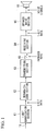
- FIG. 1 is a block diagram showing the structure of a data communication system according to the first embodiment of the present invention.
- a data transmitting apparatus and a data receiving apparatus are placed via a space 60, serving as a transmission path (communication vehicle).
- the data transmitting apparatus is formed by a 1-bit quantization section 61, a return-to-zero section 62, and a transmitting section 63
- the data receiving apparatus is formed by a receiving section 64, a speaker drive section 65, and a speaker 16.
- the 1-bit quantization section 61 converts voice signals 11 into pulse compressional waves such that the voice is transmitted through the air as air compressional waves. Namely, the output pulse trains become more dense as the level of the voice signals 11 is raised, and become more sparse as the level of the voice signals 11 is lowered.
- These pulse trains are the same as normal serial data streams, however, they are not developed serially as one group of data in several bits like those shown in FIG. 24, but, instead, are data formed by independent, individual items of data. Therefore, it is not necessary to append synchronous data showing the front position of one group of data, as was described with reference to FIG. 24.
- the received data streams have a waveform serving as compressional waves of pulses of a constant amplitude
- the speaker drive section 65 such as a low impedance driver with the waveform in this state
- the voice signal reproduction circuit that includes the speaker 16 operates as a low pass filter and voice signal reproduction becomes possible in this state.
- the same function can be obtained even if the speaker drive section is a low pass filter or a high pass filter or has a structure that includes both of these.
- infrared rays are used as a communication format for 1-bit quantized serial data streams.
- an infrared ray digital communication unit is used, then a variety of types of device can be used as the transmitting section 63 and the receiving section 64. Therefore, the transmitting section 63 and the receiving section 64 can have a structure such as that of the infrared transmitting section 13 and the infrared receiving section 14 shown in FIG. 26.
- the speaker drive section 65 can also have a structure such as that of the speaker drive section 15 shown in FIG. 26.
- Analog signals such as voice or music or digital signals such as digitized voice or music are input as voice signals 11 into the 1-bit quantization section 61.
- the 1-bit quantization section 61 converts the input analog signals or digital signals into digital signals (compressional waves of pulses) that are 1-bit data streams using a noise shaping method. A high level output is made for logical values of "1" for these digital signals that have been converted into 1-bit data streams, and a low level output is made for logical values of "0". Note that signals output from the 1-bit quantization section 61 are non-return-to-zero (NRZ) signals.
- NRZ non-return-to-zero
- the return-to-zero section 62 converts them into return-to-zero (RZ) signals having a pulse width of, for example, 10% or more and less than 90%.
- RZ return-to-zero
- the return-to-zero section 62 outputs the input non-return-to-zero signals as they are.
- the transmitting section 63 outputs signals output from the return-to-zero section 62 by infrared rays into space 60.
- the receiving section 64 receives the infrared ray signals output from the transmitting section 63 via the space 60. Signals that are received by the receiving section 64 are input into the speaker drive section 65 that drives the speaker 16, and the speaker 16 is driven by an output from the speaker drive section 65.
- the return-to-zero section 62 internally generates clocks whose duty ratio is 10% or more and less than 90%, and obtains the logical product of these clocks and the output waveform of the 1-bit quantization section 61.
- the waveform shown in FIG. 2C is obtained from the return-to-zero section 62.
- the logical product can be easily obtained by using a two input AND circuit. Signals output from the return-to-zero section 62 are input into the transmitting section 63, and the light emitting diode inside the transmitting section 63 that transmits infrared rays into the space 60 emits light in accordance with the input signals at an emission timing such as that shown in FIG. 2D.
- FIGS. 3A to 3C show relationships between a reference voltage Vref and outputs of the photo-diode inside the receiving section 64 when the same operation as is shown in FIGS. 28A to 28C was performed in the present embodiment, together with a voltage waveform output from a voltage comparator inside the receiving section 64.
- the vertical axis is voltage while the horizontal axis is time.
- the solid line in FIG. 3C shows the voltage waveform output from the voltage comparator in the receiving section 64 when "1" is input continuously, as shown in FIG. 3A.
- the broken line shown in FIG. 3C shows the voltage waveform output from the voltage comparator in the receiving section 64 when "0" is input continuously, as shown in FIG. 3B.
- the reference voltage Vref which is the average value of the output voltages of the photo-diode, is smaller than the reference voltage Vref in FIG. 28A, as is shown by the broken line in FIG. 3A.
- the reference voltage Vref is the same as the reference voltage Vref in FIG. 28B, as is shown by the broken line in FIG. 3B.
- the difference between the reference voltage Vref when "1" is continuously input and the reference voltage Vref when "0" is continuously input is smaller than is the case conventionally.
- a difference in timing when "1" is detected by the voltage comparator decreases, and it is possible to greatly reduce jitter.
- jitter is generated because it is not possible to transmit 1-bit quantized signals using existing encoding technology for jitter suppression, such as Manchester coding.
- jitter suppression such as Manchester coding.
- the present embodiment by using a return-to-zero section, jitter is suppressed and high quality voice transmission is possible. This is the major difference between the present embodiment and the conventional technology.
- the transmitting section 63 and the receiving section 64 described in the first embodiment communicate in accordance with fast IrDA physical layer (FIR), which is a physical layer of the digital data infrared ray communication standard IrDA.
- FIR fast IrDA physical layer
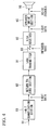
- FIG. 4 is a block diagram showing the structure of a data communication system according to the present embodiment and component elements that are the same as those shown in FIG. 1 (i.e., the first embodiment) are given the same reference symbols.
- the transmitting section 63 and the receiving section 64 are formed respectively by an IrDA transmitter 91 and an IrDA receiver 92.
- the operation of the data communication system according to the present embodiment is the same as the operation of the data communication system according to the first embodiment, apart from the fact that IrDA-FIR is used, and, therefore, a description thereof is omitted here.
- the emission peak wavelength is regulated at 870 nm
- the radiation intensity is regulated at 100 mW/sr
- the transfer speed is regulated at 1 Mbps to 4 Mbps.
- transfer at a speed of 1 Mbps or less is also possible.
- IrDA-FIR is a high speed infrared ray data transfer format that has become widely used in recent years as IrDA 1.1 in infrared ray communication between personal computers and personal digital assistants (PDA).
- PDA personal digital assistants
- the receiving section 64 described in the first embodiment receives signals transmitted from devices other than data communication systems. Therefore, if high level signals are received from another device while the transmitting section 63 is transmitting a low level signal, then this is likely to cause malfunctions. In particular, because return-to-zero signals are transferred between the data transmitting apparatus and the data receiving apparatus in each embodiment of the present invention, the low level period is longer in comparison with non-return-to-zero signals, and there is a greater likelihood than signals from other devices will be received.
- the IrDA receiver 92 is used as the receiving section 64 in the present embodiment, it is possible to remove signals at transfer speeds other than 1 Mbps to 4 Mbps using a filter incorporated in the IrDA receiver 92. Accordingly, the IrDA receiver 92 is unaffected, for example, by infrared rays transmitted from other devices such as remote controls for television or audio devices. Moreover, because IrDA transmitting and receiving units have become steadily smaller in recent years, both the data transmitting apparatus and the data receiving apparatus can be made small in size. Furthermore, in IrDA, data having 100% duty ratio is rejected, however, in each embodiment of the present invention, by providing the return-to-zero section 62 in front of the transmitting section 63 shown in FIG.
- the transmitting section 63 can be realized without any special circuitry or the like having to be added other than the IrDA transmitter 91.
- a filter be provided inside the receiving section 64, in the same way as in the IrDA receiver, even if a device other than an IrDA transmitter or receiver is used as the transmitting or receiving sections.
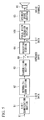
- FIG. 5 is a block diagram showing the structure of a data communication system according to the third embodiment of the present invention.
- a pulse width extension section 101 is placed between the receiving section 64 and the speaker drive section 65 of the structure shown in FIG. 1.
- pulse width extension section 101 pulse widths that have been narrowed by the return-to-zero section 62 are extended so as to be converted into waveforms having 100% duty ratio like the original non-return-to-zero signals or having waveforms with close to 100% duty ratio.
- the signals then have the same waveform as the output of the 1-bit quantization section 61.
- the pulse width extension section 101 is provided in addition to the return-to-zero section 62, and jitter can be reduced by reducing the duty ratio of transferred pulse signals by the return-to-zero section 62.
- the pulse width of signals input into the speaker drive section 65 is extended by the pulse width extension section 101 enabling the maximum voice signal sound pressure to be obtained.
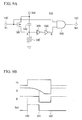
- FIG. 6 is a circuit diagram shown a specific example of the pulse width extension section 101.
- the operation of the circuit shown in FIG. 6 will now be described with reference also made to the waveform diagram in FIG. 7.
- the vertical axis is voltage
- the horizontal axis is time
- the solid line is the voltage waveform of an input In (i.e., an output from the receiving section 64) supplied to an input terminal 111 shown in FIG. 6
- the broken line is the voltage waveform of the output Out that is output to the speaker drive section 65 from an output terminal 113 shown in FIG. 6,
- the long - short dash line is the voltage waveform at the point A in FIG. 6.
- the input In is taken as a low level
- the potential at the point A is taken as a high level
- the output Out is taken as a low level.
- a capacitor 115 is charged through a resistor 114 by a power supply voltage Vdd that is applied to a power supply terminal 110, so that the charge is accumulated in the capacitor 115.
- Vdd power supply voltage
- an NMOS transistor 116 is turned on and the charge that was stored in the capacitor 115 is discharged.
- the potential at the point A changes to a GND level and the output Out changes to a high level.
- the input In changes to a low level and the NMOS transistor 116 is turned off.
- the capacitor 115 then continues to be charged in accordance with a time constant of a CR circuit formed by the capacitor 115 and the resistor 114, so that the potential at the point A continues to rise.
- the output Out changes to a low level.
- the pulse width extension section 101 can be realized if the time constant of the CR circuit is adjusted so that the pulse width B of the output Out is the same as if the duty ratio was 100% like the signals output from the 1-bit quantization section 61.
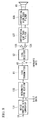
- FIG. 8 is a block diagram showing the structure of a data communication system according to the fourth embodiment of the present invention.
- the same reference symbols are given to component elements that are identical to those appearing in FIG. 1 (i.e., in the first embodiment) and FIG. 4 (i.e., in the second embodiment).
- the component elements other than the speaker 16 that were described in the first embodiment in FIG. 1 are formed into specific circuits. Namely, in FIG. 8, a noise shaping A/D converter 131, a return-to-zero circuit 132, the IrDA transmitter 91 (see FIG. 4), and the IrDA receiver 92 (see FIG.
- the speaker drive section 65 of FIG. 1 is realized by a buffer 135, an inverter 136, a differential low pass filter 137, and a differential high pass filter 138.
- the noise shaping A/D converter 131 converts analog voice signals 11 such as voice or music into digital 1-bit data streams using a noise shaping method.
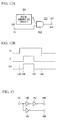
- the return-to-zero circuit 132 can be realized, for example, by the circuit shown in FIG. 9A.
- the voltage waveforms of each section in the return-to-zero circuit 132 in this case are shown in FIG. 9B.
- the pulse width of return-to-zero signals output from the return-to-zero circuit 132 is determined by an RC time constant.
- the input In supplied to an input terminal 140 is taken as a low level.
- the potential at the point A becomes a high level
- the potential at the point B also becomes a high level via the inverters 144 and 145. Because the input In at this time is at a low level, the output Out that is output from an AND circuit 146 to an output terminal 147 is at a low level.
- the AND circuit 146 outputs a high level as the output Out.
- the PMOS transistor 141 is turned off, a capacitor 143 is charged by a time constant of an RC circuit formed by the resistor 142 and the capacitor 143, and the potential at the point A is gradually reduced.
- the output from the inverter 144 changes to a high level and the potential at the point B, which is the output from the inverter 145 changes to a low level.
- the output Out is restored to a low level. Subsequently, when the input In changes to a low level at the timing t42, the same operation as was described in the initial state is performed and a state that is the same as the initial state is restored.
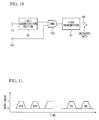
- a structure such as that shown in FIG. 10 may be employed.
- a structure such as that shown in FIG. 10 may be employed.
- the clock signals 101 are at a low level, "0" is always output regardless of the output from the 1-bit quantization section 61.
- FIG. 11 it is possible to make a duty ratio of an incoming data stream, for example, into a 50% duty ratio even when signals having a 100% duty ratio (for example, an NRZ signal) arrive.
- the clock signals 101 can be generated, for example, by a pulse generating circuit 151, such as is shown in FIG. 12A, and the voltage waveform in each section in FIG. 12A in this case is shown in FIG. 12B.
- the pulse width of the output Out is determined by the pulse width of clock signals generated by the pulse generating circuit 151. Namely, the input In from the noise shaping A/D converter 131 is at a high level from the timing t45 through to the timing t48, and the pulse generating circuit 151 outputs high level pulses from the timing t46 through to the timing t47 to the point C. Therefore, the output Out that is output to the IrDA transmitter 132 is at a high level from the timing t46 through to the timing t47.
- the differential low pass filter 137 and the differential high pass filter 138 are both filters for dealing with voice and music bands (i.e., for audible bands) and the specific structures and operations thereof are described further in the fifth embodiment.
- Voice signals 11 are input into the noise shaping A/D converter 131.
- the noise shaping A/D converter 131 converts the voice signals 11 into non-return-to-zero digital signals of a 1-bit data stream and then outputs these signals.
- These non-return-to-zero digital signals of a 1-bit data stream are input into the return-to-zero circuit 132 where they are converted into return-to-zero signals.
- the output of this return-to-zero circuit 132 is input into the IrDA transmitter 91, and the IrDA transmitter 91 emits infrared rays having a wavelength of 870 nm in accordance with IrDA -FIR.
- an IrDA transmitting and receiving unit that satisfies standards such as IrDA 1.1 and the like can be used as the IrDA transmitter 91, and the emitted infrared rays are received by an IrDA receiver 92 that satisfies standards such as IrDA 1.1 in the same way as the IrDA transmitter 91.
- the reception output of the IrDA receiver 92 is then input into the buffer 135 and the inverter 136 and are converted into differential signals.
- Outputs from the buffer 135 and the inverter 136 are then input into the differential low pass filter 137 and shaped quantization noise (described below in detail) is removed.
- the output of the differential low pass filter 137 is input into the differential high pass filter 138 and the pulse frequency signal component (described below in detail) is removed.
- the output from the differential high pass filter 138 is then input into the speaker 16 and voice signals are output from the speaker 16.
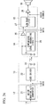
- the buffer 135 and the inverter 136 can be formed by three inverters 162, 163, and 164 as is shown in FIG. 13. Of these inverters, the inverter 162 and the inverter 163 correspond to the buffer 135 shown in FIG. 8, and the inverter 164 corresponds to the inverter 136 in FIG. 8.
- the present embodiment is a specific structural example of the differential low pass filter 137 and the differential high pass filter 138 shown in FIG. 8 (i.e., the fourth embodiment).
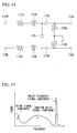
- FIG. 14 is a circuit diagram showing the structure of the differential low pass filter 137 and the differential high pass filter 138 of the fifth embodiment according to the present invention.
- a resistor 171A, a coil 172A, and a capacitor 173A are connected in series between a differential input terminal 170A and a differential output terminal 174A.
- a resistor 171B, a coil 172B, and a capacitor 173B are connected in series between a differential input terminal 170B and a differential output terminal 174B.
- a capacitor 175 is placed between the connection point of the coil 172A and the capacitor 173A and the connection point of the coil 172B and the capacitor 173B.
- a resistor 176A is placed between the differential output terminal 174A and the GND, and a resistor 176B is connected between the differential output terminal 174B and the GND.
- This circuit is a high pass filter and a low pass filter that uses R, L, and C elements, and, by applying it to the data receiving apparatus according to each embodiment of the present invention, the special effects described below, which are not obtained from the conventional technology are manifested.
- the waveform of voice signals 11 converted by the noise shaping A/D converter 131 and the return-to-zero circuit 132 have a voice signal component, a shaping noise signal component, and a pulse frequency signal component as spectrum components, as is shown in FIG. 15.
- the power of the pulse frequency signal component is one digit larger than the power of the other signal components and because the pulse frequency signal component does not contain a voice signal component, if it is consumed as power then it ends up becoming reactive power.
- an inductance component made up of the coil 172A and the coil 172B is inserted. Because the frequency band of the pulse frequency signal component is several MHz, impedance that includes inductance is extremely large in this frequency band. Accordingly, in this frequency band, current does not flow by the operation of the coil 172A and the coil 172B and the power consumption of this pulse frequency signal component is extremely small.
- the resistor 171A and the resistor 171B are each connected in serial with the coil 172A and the coil 172B, and are positioned before the capacitor 175 as seen from the differential input terminals 170A and 170B. Therefore, the current of the pulse frequency signal component flowing in the resistor 171A and the resistor 171B is restricted to an extremely small quantity by the coil 172A and the coil 172B, and there is no power consumption by the pulse frequency signal component in the resistor 171 A and the resistor 171B.
- the speaker drive section 65 is formed by the buffer 135 and the inverter 136, as is the case in the fourth embodiment, then when the IrDA receiver 92 is not receiving light, the output of the buffer 135 is the power supply level and the output of the inverter 136 is the GND level.
- dynamic type speakers that are normally used are equivalent to inductance components, they show extremely low impedance to direct current.
- the coil 172A and the coil 172B also show low resistance to direct current, then when the IrDA receiver 92 is not receiving signals a large direct current ends up flowing in the speaker 16 and in the buffer 135 and the inverter 136 that form the speaker drive section. Therefore, in the present embodiment, a high pass filter is formed by the capacitor 173A and the capacitor 173B and by the resistor 176A and the resistor 176B so as to prevent the flow of direct current.
- FIG. 16 a specific circuit obtained by replacing the differential low pass filter 137 and the differential high pass filter 138 in FIG. 8 is shown in FIG. 16. Note that, in FIG. 16, the same reference symbols have been given to component elements that are the same as those in FIG. 14. As is clear from FIG. 16, a differential high pass filter formed by the capacitor 173A and the capacitor 173B and by the resistor 176A and the resistor 176B is placed on the side of the differential input terminals 170A and 170B, and a differential low pass filter formed by the resistor 171A and the resistor 171B and by the coil 172A and the coil 172B and by the capacitor 175 is placed on the side of the differential output terminals 174A and 174B.
- the differential low pass filter 137 and the differential high pass filter 138 be positioned in front of the speaker 16, however, the present invention is not limited to this structure.
- a low pass filter or high pass filter which are formed by a capacitor and a resistor or coil that have a structure different from those shown in FIGS. 14 and 16, or to insert both a high pass filter and a low pass filter between the speaker drive section 65 and the speaker 16.
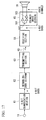
- FIG. 17 it is also possible to omit the low pass filter or high pass filter and to connect the speaker drive section 65 having a structure such as that shown in FIG. 13, for example, directly to the speaker 16.
- the speaker drive section 65 having a structure such as that shown in FIG. 13, for example, directly to the speaker 16.
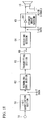
- the speaker 16 is driven differentially, however, the present invention is not limited to this structure, and it is also possible to form the speaker drive section 65 using, for example, just one inverter 261, as is shown in FIG. 18. In this case, it is sufficient if the speaker 16 is driven just by pulse trains output from the receiving section 64 and, when driving a low input impedance speaker, this is done extremely simply by one inverter.
- the duty ratio of return-to-zero signals output from the return-to-zero section 62 was 10% or more and less than 90%, however, the duty ratio is not limited to this range and, theoretically, if the duty ratio is anything other than 0% and 100%.
- the duty ratio of signals output from the return-to-zero section 62 or from the return-to-zero circuit 132 is made as small as possible and is restricted, for example, 10% or more and 50% or less. This allows the drive power of the light emitting diode provided inside the IrDA transmitter 91 to be considerably reduced.
- power consumption of 1W or more is required if 100% duty ratio infrared rays are emitted using an IrDA 1.1 Standard infrared ray emitter.
- the duty ratio of signals output from the return-to-zero circuit 132 is set at 25%, it is possible to reduce the power consumption of the infrared ray emitter to one quarter, namely, to 250 mW. This is a major feature obtained by using the return-to-zero section or return-to-zero circuit in each of the above embodiments that is not available from the conventional technology.
- the duty ratio of signals output from the return-to-zero section 62 or the return-to-zero circuit 132 is made less than 40%, an even better noise suppression effect is obtained. Accordingly, it is preferable that the duty ratio be 5% or more and less than 40%.
- the duty ratio is ⁇ (m/2 n ) x 100 ⁇ % (wherein m and n are natural numbers that satisfy in ⁇ 2 n ), for example, 75%, 50%, or 25%.
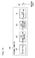
- FIG. 19 is a block diagram showing the structure of the data transmitting apparatus of the data communication system according to the present embodiment. Note that the structure of the data receiving apparatus is the same as in each of the above described embodiments.
- a personal computer 190 has a voice file 191 obtained by digitizing voice or music stored on internal memory or on a storage medium such as a disk; a 1-bit quantization program 192 that reads digital data stored in the voice file 191 and performs noise shaping processing using a software program; a zero insertion program 193 that inserts data representing a "0" for each bit of the 1-bit data streams that have undergone noise shaping processing; and an IrDA transmitter 91 the same as that shown in FIG. 8. Specifically, the zero insertion program 193 inserts data representing a "0" before each bit of the 1-bit data streams. Alternatively, the zero insertion program 193 inserts data representing a "0" after each bit of the 1-bit data streams.
- Output data that has been processed by the zero insertion program 193 is output from the IrDA transmitter 91 at twice the speed of the noise shaping frequency. As a result, it is possible to output 1-bit data streams that have undergone noise shaping processing and having a duty ratio of 50% from the IrDA transmitter 91 in accordance with FIR.
- a data transmitting apparatus can be achieved without adding I/O devices using software that operates on a personal computer. Namely, it is possible to form the data transmission apparatuses of each of the above described embodiments simply by installing application software having the above described functions on a personal computer without having to provide special hardware.
- the output of the zero insertion program 193 is supplied directly to the IrDA transmitter 91, however, the present invention is not limited to this structure.
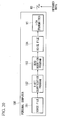
- the data stored in the sound file 194 is then read at a suitable timing, and is transmitted from the IrDA transmitter 91.
- the 1-bit quantization section 61 and the return-to-zero section 62 are achieved by software programs, however, it is also possible for the return-to-zero section 62 alone to be achieved by a software program.
- the 1-bit quantization program 192 and/or the zero insertion program 193 can be recorded on a computer readable medium, and for the programs recorded on this recording medium to be loaded on a computer system and to be executed by the computer system.
- a computer system includes OS and hardware such as peripheral devices.
- Computer readable recording medium refers to a transportable medium such as a flexible disk, a magneto-optical disk, ROM, a CD-ROM, and the like, or to a storage apparatus such as a hard disk installed in a computer system.
- Computer readable recording medium also includes mediums that hold programs for a certain period of time such as volatile memory (RAM) in a computer system which is a server or a client when programs are transmitted via a communication line such as a telephone line or a network such as the Internet.
- RAM volatile memory
- each of the above programs may also be transferred from a computer system having a storage apparatus or the like on which these programs are stored via a transfer medium, or via a transfer wave in the transfer medium to another computer system.
- the transfer medium that transfers the programs is a medium having a function of transferring information such as a communication line like a telephone or a network such as the Internet.
- the above programs may also be designed to perform a portion of the aforementioned function. They may also be what is known as a differential file (differential program) that can achieve these functions in combination with a program that is already recorded on a computer system.
- a differential file Differential program
- the present invention is not limited to this structure and, instead of infrared rays, it is possible to use light (i.e., visible light), ultraviolet rays, radio waves, and magnetic waves and the like. Namely, it is sufficient if the transmitting section 63 shown in FIG. 1 modulates 1-bit digital data streams using a predetermined modulation format and then emits light, ultraviolet rays, radio waves, and magnetic waves or the like into space or the like. Moreover, it is sufficient if the receiving section 64 shown in FIG. 1 receives light, ultraviolet rays, radio waves, and magnetic waves or the like that have been emitted into space or the like, and demodulates these so as to obtain the original 1-bit digital data streams.
- light i.e., visible light
- ultraviolet rays i.e., visible light
- the transmitting section 63 shown in FIG. 1 modulates 1-bit digital data streams using a predetermined modulation format and then emits light, ultraviolet rays, radio waves, and magnetic waves or the like into space or the like.
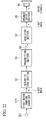
- FIG. 21 is a block diagram showing the structure of the data communication system according to the ninth embodiment of the present invention.
- a transmitter having an RF transmission circuit and antenna 263 that modulates signals output from the return-to-zero circuit 62 using a format such as FSK, amplitude key shifting (ASK), phase key shifting (PSK) or the like and then transmits these signals is used as the transmitting section 63 shown in FIG. 1.
- a receiver having an RF reception circuit and antenna 264 that receives signals and demodulates them using the FSK, ASK, or PSK formats is used as the receiving section 64 shown in FIG. 1.
- This transmitter and receiver can be structured using conventional radio wave based data transmitting and receiving units.
- the operation of the data communication system of the present embodiment is the same as the operation of the data communication system of the first embodiment except that radio waves are used instead of the infrared rays used in the first embodiment.
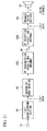
- FIG. 22 is a block diagram showing the structure of the data communication system according to the tenth embodiment of the present invention.
- input into the data communication system is not analog signals, but is made up by digital signals of several bits (the digital voice signals 251 in FIG. 22) obtained by performing binary conversion on analog signals such as voice, music, and the like.
- a 1-bit noise shaping quantizer 271 that converts digital signals of several bits into 1-bit digital data streams is used as the 1-bit quantization section 61 shown in FIG. 1.
- the operation of the data communication system of the present embodiment is the same as the operation of the data communication system of the first embodiment except that digital signals of several bits are input.
Landscapes
- Physics & Mathematics (AREA)
- Engineering & Computer Science (AREA)
- Computer Networks & Wireless Communication (AREA)
- Signal Processing (AREA)
- Electromagnetism (AREA)
- Spectroscopy & Molecular Physics (AREA)
- Optical Communication System (AREA)
- Dc Digital Transmission (AREA)
Applications Claiming Priority (2)
| Application Number | Priority Date | Filing Date | Title |
|---|---|---|---|
| JP2002271100 | 2002-09-18 | ||
| JP2002271100 | 2002-09-18 |
Publications (1)
| Publication Number | Publication Date |
|---|---|
| EP1401166A1 true EP1401166A1 (de) | 2004-03-24 |
Family
ID=31944542
Family Applications (1)
| Application Number | Title | Priority Date | Filing Date |
|---|---|---|---|
| EP03103409A Withdrawn EP1401166A1 (de) | 2002-09-18 | 2003-09-16 | Verfahren und Vorrichtung zur Übertragung von Sprach- und Musikdaten mittels RZ-Signalen |
Country Status (3)
| Country | Link |
|---|---|
| US (1) | US20040062362A1 (de) |
| EP (1) | EP1401166A1 (de) |
| CN (1) | CN1496076A (de) |
Families Citing this family (58)
| Publication number | Priority date | Publication date | Assignee | Title |
|---|---|---|---|---|
| US6815944B2 (en) * | 2002-01-31 | 2004-11-09 | Allegro Microsystems, Inc. | Method and apparatus for providing information from a speed and direction sensor |
| DE602004019040D1 (de) * | 2003-12-19 | 2009-03-05 | Ibm | Verbesserungen für Datenrückgewinnungsschaltungen mit Überabtastung zu Wahl des besten Datenabtastwertes |
| US7365530B2 (en) * | 2004-04-08 | 2008-04-29 | Allegro Microsystems, Inc. | Method and apparatus for vibration detection |
| US7689176B2 (en) * | 2005-03-07 | 2010-03-30 | Codman NeuroSciences Sárl | Telemetry system employing DC balanced encoding |
| US7253614B2 (en) * | 2005-03-21 | 2007-08-07 | Allegro Microsystems, Inc. | Proximity detector having a sequential flow state machine |
| JP2007067569A (ja) * | 2005-08-29 | 2007-03-15 | Sharp Corp | 赤外線通信受信機 |
| JP2007124574A (ja) | 2005-10-31 | 2007-05-17 | Sharp Corp | D級増幅器およびそれを用いた赤外線データ受信装置 |
| JP2007158841A (ja) * | 2005-12-06 | 2007-06-21 | Sharp Corp | 受信機および赤外線ワイヤレスイヤホン |
| US8050572B2 (en) * | 2007-05-29 | 2011-11-01 | Sharp Kabushiki Kaisha | Receiver and electronic device |
| US9823090B2 (en) | 2014-10-31 | 2017-11-21 | Allegro Microsystems, Llc | Magnetic field sensor for sensing a movement of a target object |
| US8787440B2 (en) * | 2008-07-25 | 2014-07-22 | Qualcomm Incorporated | Determination of receive data values |
| US8624588B2 (en) * | 2008-07-31 | 2014-01-07 | Allegro Microsystems, Llc | Apparatus and method for providing an output signal indicative of a speed of rotation and a direction of rotation as a ferromagnetic object |
| US8022692B2 (en) * | 2009-01-19 | 2011-09-20 | Allegro Microsystems, Inc. | Direction detection sensor |
| US20110148604A1 (en) * | 2009-12-17 | 2011-06-23 | Spin Master Ltd. | Device and Method for Converting a Computing Device into a Remote Control |
| CN102386977A (zh) * | 2011-10-20 | 2012-03-21 | 航天科工深圳(集团)有限公司 | 一种用于光纤传输的数据发送、接收方法、装置及设备 |
| US9817078B2 (en) | 2012-05-10 | 2017-11-14 | Allegro Microsystems Llc | Methods and apparatus for magnetic sensor having integrated coil |
| US9329057B2 (en) | 2012-05-31 | 2016-05-03 | Allegro Microsystems, Llc | Gear tooth sensor with peak and threshold detectors |
| US8754640B2 (en) | 2012-06-18 | 2014-06-17 | Allegro Microsystems, Llc | Magnetic field sensors and related techniques that can provide self-test information in a formatted output signal |
| US10495699B2 (en) | 2013-07-19 | 2019-12-03 | Allegro Microsystems, Llc | Methods and apparatus for magnetic sensor having an integrated coil or magnet to detect a non-ferromagnetic target |
| US9810519B2 (en) | 2013-07-19 | 2017-11-07 | Allegro Microsystems, Llc | Arrangements for magnetic field sensors that act as tooth detectors |
| US10145908B2 (en) | 2013-07-19 | 2018-12-04 | Allegro Microsystems, Llc | Method and apparatus for magnetic sensor producing a changing magnetic field |
| US9720054B2 (en) | 2014-10-31 | 2017-08-01 | Allegro Microsystems, Llc | Magnetic field sensor and electronic circuit that pass amplifier current through a magnetoresistance element |
| US9719806B2 (en) | 2014-10-31 | 2017-08-01 | Allegro Microsystems, Llc | Magnetic field sensor for sensing a movement of a ferromagnetic target object |
| US10712403B2 (en) | 2014-10-31 | 2020-07-14 | Allegro Microsystems, Llc | Magnetic field sensor and electronic circuit that pass amplifier current through a magnetoresistance element |
| US9823092B2 (en) | 2014-10-31 | 2017-11-21 | Allegro Microsystems, Llc | Magnetic field sensor providing a movement detector |
| US9524794B1 (en) * | 2015-08-10 | 2016-12-20 | Sandisk Technologies Llc | Constrained data shaping |
| CN105654014B (zh) * | 2015-12-30 | 2018-02-02 | 广州中大微电子有限公司 | 一种可兼容高低速信号解调的射频信号解调电路 |
| CN105743577A (zh) * | 2016-01-29 | 2016-07-06 | 杭州电子科技大学 | 基于锁相环的可见光音频传输系统 |
| US10495700B2 (en) | 2016-01-29 | 2019-12-03 | Allegro Microsystems, Llc | Method and system for providing information about a target object in a formatted output signal |
| EP4067908B1 (de) | 2016-05-17 | 2025-11-12 | Allegro MicroSystems, LLC | Magnetfeldsensor und verfahren zum betreiben eines magnetfeldsensors |
| US10260905B2 (en) | 2016-06-08 | 2019-04-16 | Allegro Microsystems, Llc | Arrangements for magnetic field sensors to cancel offset variations |
| US10041810B2 (en) | 2016-06-08 | 2018-08-07 | Allegro Microsystems, Llc | Arrangements for magnetic field sensors that act as movement detectors |
| US10012518B2 (en) | 2016-06-08 | 2018-07-03 | Allegro Microsystems, Llc | Magnetic field sensor for sensing a proximity of an object |
| CN106375255B (zh) * | 2016-08-31 | 2019-06-07 | 成都九洲电子信息系统股份有限公司 | 基于fpga的pr_ask调制方法 |
| JP6764943B2 (ja) * | 2016-12-12 | 2020-10-07 | 株式会社Fuji | 対基板作業システム |
| CN106803762B (zh) * | 2016-12-28 | 2019-03-05 | 中国北方车辆研究所 | 一种应用于数字通信的编码方法 |
| US10996289B2 (en) | 2017-05-26 | 2021-05-04 | Allegro Microsystems, Llc | Coil actuated position sensor with reflected magnetic field |
| US10324141B2 (en) | 2017-05-26 | 2019-06-18 | Allegro Microsystems, Llc | Packages for coil actuated position sensors |
| US11428755B2 (en) | 2017-05-26 | 2022-08-30 | Allegro Microsystems, Llc | Coil actuated sensor with sensitivity detection |
| US10837943B2 (en) | 2017-05-26 | 2020-11-17 | Allegro Microsystems, Llc | Magnetic field sensor with error calculation |
| US10641842B2 (en) | 2017-05-26 | 2020-05-05 | Allegro Microsystems, Llc | Targets for coil actuated position sensors |
| US10310028B2 (en) | 2017-05-26 | 2019-06-04 | Allegro Microsystems, Llc | Coil actuated pressure sensor |
| US10866117B2 (en) | 2018-03-01 | 2020-12-15 | Allegro Microsystems, Llc | Magnetic field influence during rotation movement of magnetic target |
| US10656170B2 (en) | 2018-05-17 | 2020-05-19 | Allegro Microsystems, Llc | Magnetic field sensors and output signal formats for a magnetic field sensor |
| US11255700B2 (en) | 2018-08-06 | 2022-02-22 | Allegro Microsystems, Llc | Magnetic field sensor |
| US10823586B2 (en) | 2018-12-26 | 2020-11-03 | Allegro Microsystems, Llc | Magnetic field sensor having unequally spaced magnetic field sensing elements |
| US11061084B2 (en) | 2019-03-07 | 2021-07-13 | Allegro Microsystems, Llc | Coil actuated pressure sensor and deflectable substrate |
| US10955306B2 (en) | 2019-04-22 | 2021-03-23 | Allegro Microsystems, Llc | Coil actuated pressure sensor and deformable substrate |
| US11125590B2 (en) | 2019-05-07 | 2021-09-21 | Allegro Microsystems, Llc | System and method for vibration detection with direction change response immunity using a magnetic field sensor |
| US11029176B2 (en) | 2019-05-07 | 2021-06-08 | Allegro Microsystems, Llc | System and method for vibration detection with no loss of position information using a magnetic field sensor |
| US11237020B2 (en) | 2019-11-14 | 2022-02-01 | Allegro Microsystems, Llc | Magnetic field sensor having two rows of magnetic field sensing elements for measuring an angle of rotation of a magnet |
| US11280637B2 (en) | 2019-11-14 | 2022-03-22 | Allegro Microsystems, Llc | High performance magnetic angle sensor |
| TWI718029B (zh) * | 2020-03-17 | 2021-02-01 | 宏碁股份有限公司 | 加速放電裝置 |
| US11262422B2 (en) | 2020-05-08 | 2022-03-01 | Allegro Microsystems, Llc | Stray-field-immune coil-activated position sensor |
| US11493361B2 (en) | 2021-02-26 | 2022-11-08 | Allegro Microsystems, Llc | Stray field immune coil-activated sensor |
| US11578997B1 (en) | 2021-08-24 | 2023-02-14 | Allegro Microsystems, Llc | Angle sensor using eddy currents |
| US12449279B2 (en) | 2024-02-07 | 2025-10-21 | Allegro Microsystems, Llc | Dynamic resolution sensor |
| US12523717B2 (en) | 2024-02-15 | 2026-01-13 | Allegro Microsystems, Llc | Closed loop magnetic field sensor with current control |
Citations (4)
| Publication number | Priority date | Publication date | Assignee | Title |
|---|---|---|---|---|
| EP0585030A1 (de) * | 1992-08-18 | 1994-03-02 | Nokia Mobile Phones Ltd. | Infrarotverbindung zwischen einem Sendeempfänger und einem externen Gerät |
| EP0957596A1 (de) * | 1994-06-30 | 1999-11-17 | AT&T Corp. | Datenkodierter optischer Impulsgeber |
| EP0991286A2 (de) * | 1998-09-14 | 2000-04-05 | Nec Corporation | Tragbares Telephon und Kraftfahrzeugsystem |
| US20020030871A1 (en) * | 2000-04-04 | 2002-03-14 | Anderson Marlyn J. | Low power portable communication system with wireless receiver and methods regarding same |
Family Cites Families (11)
| Publication number | Priority date | Publication date | Assignee | Title |
|---|---|---|---|---|
| US4627090A (en) * | 1982-07-19 | 1986-12-02 | Smith Engineering | Audio frequency multiplication device |
| US4829299A (en) * | 1987-09-25 | 1989-05-09 | Dolby Laboratories Licensing Corporation | Adaptive-filter single-bit digital encoder and decoder and adaptation control circuit responsive to bit-stream loading |
| US4833418A (en) * | 1988-09-01 | 1989-05-23 | Archive Corporation | Compensation circuit for nullifying differential offset voltage and regulating common mode voltage of differential signals |
| US5008964A (en) * | 1990-02-09 | 1991-04-23 | Janet C. Dean | Child's toilet |
| SE465144B (sv) * | 1990-06-26 | 1991-07-29 | Ericsson Ge Mobile Communicat | Saett och anordning foer behandling av en analog signal |
| JP2828543B2 (ja) * | 1991-08-02 | 1998-11-25 | シャープ株式会社 | スピーカ駆動回路 |
| US5347587A (en) * | 1991-11-20 | 1994-09-13 | Sharp Kabushiki Kaisha | Speaker driving device |
| JPH088831A (ja) * | 1994-06-22 | 1996-01-12 | Fujitsu Ltd | 光送信機 |
| JP3615285B2 (ja) * | 1995-09-29 | 2005-02-02 | 日本バーブラウン株式会社 | 差動型フィルター回路及びその集積回路構造 |
| JPH1051888A (ja) * | 1996-05-28 | 1998-02-20 | Sony Corp | スピーカ装置および音声再生システム |
| US6064699A (en) * | 1997-07-07 | 2000-05-16 | Golden Eagle Electronics Manufactory Ltd. | Wireless speaker system for transmitting analog and digital information over a single high-frequency channel |
-
2003
- 2003-09-16 EP EP03103409A patent/EP1401166A1/de not_active Withdrawn
- 2003-09-16 CN CNA031272967A patent/CN1496076A/zh active Pending
- 2003-09-16 US US10/663,282 patent/US20040062362A1/en not_active Abandoned
Patent Citations (4)
| Publication number | Priority date | Publication date | Assignee | Title |
|---|---|---|---|---|
| EP0585030A1 (de) * | 1992-08-18 | 1994-03-02 | Nokia Mobile Phones Ltd. | Infrarotverbindung zwischen einem Sendeempfänger und einem externen Gerät |
| EP0957596A1 (de) * | 1994-06-30 | 1999-11-17 | AT&T Corp. | Datenkodierter optischer Impulsgeber |
| EP0991286A2 (de) * | 1998-09-14 | 2000-04-05 | Nec Corporation | Tragbares Telephon und Kraftfahrzeugsystem |
| US20020030871A1 (en) * | 2000-04-04 | 2002-03-14 | Anderson Marlyn J. | Low power portable communication system with wireless receiver and methods regarding same |
Also Published As
| Publication number | Publication date |
|---|---|
| US20040062362A1 (en) | 2004-04-01 |
| CN1496076A (zh) | 2004-05-12 |
Similar Documents
| Publication | Publication Date | Title |
|---|---|---|
| EP1401166A1 (de) | Verfahren und Vorrichtung zur Übertragung von Sprach- und Musikdaten mittels RZ-Signalen | |
| EP2461485B1 (de) | Vorrichtung und Verfahren zum Senden und Empfangen von High-Fidelity-Audio unter Verwendung eines einzigen Drahts | |
| US20040109510A1 (en) | Technique for utilizing spare bandwidth resulting from the use of a transition-limiting code in a multi-level signaling system | |
| EP2793424B1 (de) | Host-Kommunikationsschaltung, Kommunikationssystem und Kommunikationsverfahren | |
| EP1330083B1 (de) | Digitaler datensender | |
| EP1250026A1 (de) | Nahbereich-Datenübertragung für Kommunikationsgeräte | |
| CN101729471A (zh) | 广播通信系统的模拟信号和数字信号复合传输通信方法 | |
| CN103187999A (zh) | 信息传输方法及装置、移动终端 | |
| US7742542B2 (en) | Phase correlated quadrature amplitude modulation | |
| JP3866232B2 (ja) | データ通信方法,データ送信装置およびデータ受信装置,ならびにデータ送信プログラム | |
| JP3065919B2 (ja) | Fm変復調システム及びfm変調器 | |
| EP1278318A2 (de) | System zur drahtlosen Audioübertragung | |
| US6473469B1 (en) | Local communication system and apparatus for use therein | |
| US5625645A (en) | Differential pulse encoding and decoding for binary data transmissions | |
| JP2003513521A (ja) | パルスの復号化を用いて通信する方法および装置 | |
| US7260151B2 (en) | Dual phase pulse modulation system | |
| US5058131A (en) | Transmitting high-bandwidth signals on coaxial cable | |
| JP2000134269A5 (de) | ||
| Ziemer | Pulse Modulation | |
| US6944212B2 (en) | Method and apparatus for the spectrally efficient encoding and decoding of discrete data into and from analog waveforms | |
| JP2001069181A (ja) | ディジタルデータ伝送方法およびこの方法を実施する装置 | |
| EP0381464B1 (de) | Übertragung von Signalen mit hoher Bandbreite über ein Koaxialkabel | |
| WO2005074219A1 (ja) | データ送信装置、データ受信装置、伝送路符号化方法および復号方法 | |
| JPH0774648A (ja) | 通信装置 | |
| JP2005094049A (ja) | 双方向光送受信装置及び双方向光伝送システム |
Legal Events
| Date | Code | Title | Description |
|---|---|---|---|
| PUAI | Public reference made under article 153(3) epc to a published international application that has entered the european phase |
Free format text: ORIGINAL CODE: 0009012 |
|
| 17P | Request for examination filed |
Effective date: 20030916 |
|
| AK | Designated contracting states |
Kind code of ref document: A1 Designated state(s): AT BE BG CH CY CZ DE DK EE ES FI FR GB GR HU IE IT LI LU MC NL PT RO SE SI SK TR |
|
| AX | Request for extension of the european patent |
Extension state: AL LT LV MK |
|
| 17Q | First examination report despatched |
Effective date: 20040510 |
|
| AKX | Designation fees paid |
Designated state(s): DE FR GB |
|
| STAA | Information on the status of an ep patent application or granted ep patent |
Free format text: STATUS: THE APPLICATION IS DEEMED TO BE WITHDRAWN |
|
| 18D | Application deemed to be withdrawn |
Effective date: 20100401 |