EP1403676A1 - Appareil de mesure de largeurs de structure - Google Patents
Appareil de mesure de largeurs de structure Download PDFInfo
- Publication number
- EP1403676A1 EP1403676A1 EP03021531A EP03021531A EP1403676A1 EP 1403676 A1 EP1403676 A1 EP 1403676A1 EP 03021531 A EP03021531 A EP 03021531A EP 03021531 A EP03021531 A EP 03021531A EP 1403676 A1 EP1403676 A1 EP 1403676A1
- Authority
- EP
- European Patent Office
- Prior art keywords
- condenser
- measuring device
- microlens array
- array arrangement
- width measuring
- Prior art date
- Legal status (The legal status is an assumption and is not a legal conclusion. Google has not performed a legal analysis and makes no representation as to the accuracy of the status listed.)
- Granted
Links
- 210000001747 pupil Anatomy 0.000 claims abstract description 43
- 230000003287 optical effect Effects 0.000 claims abstract description 35
- 238000005259 measurement Methods 0.000 claims abstract description 24
- 238000007493 shaping process Methods 0.000 claims abstract description 11
- 238000003491 array Methods 0.000 claims description 9
- 230000003595 spectral effect Effects 0.000 claims description 3
- 238000001228 spectrum Methods 0.000 claims description 3
- 230000005855 radiation Effects 0.000 abstract description 3
- 238000005286 illumination Methods 0.000 description 13
- 238000009826 distribution Methods 0.000 description 10
- 238000000265 homogenisation Methods 0.000 description 7
- 238000004519 manufacturing process Methods 0.000 description 5
- 230000000694 effects Effects 0.000 description 4
- 239000004065 semiconductor Substances 0.000 description 4
- 238000011156 evaluation Methods 0.000 description 3
- 238000005469 granulation Methods 0.000 description 2
- 230000003179 granulation Effects 0.000 description 2
- 238000003384 imaging method Methods 0.000 description 2
- 238000007689 inspection Methods 0.000 description 2
- 238000012935 Averaging Methods 0.000 description 1
- 241000276498 Pollachius virens Species 0.000 description 1
- 230000015572 biosynthetic process Effects 0.000 description 1
- 230000001427 coherent effect Effects 0.000 description 1
- 238000000034 method Methods 0.000 description 1
- 238000012856 packing Methods 0.000 description 1
- 238000001454 recorded image Methods 0.000 description 1
- 230000000630 rising effect Effects 0.000 description 1
- 238000000926 separation method Methods 0.000 description 1
- 239000000758 substrate Substances 0.000 description 1
- 230000004304 visual acuity Effects 0.000 description 1
Images



Classifications
-
- G—PHYSICS
- G01—MEASURING; TESTING
- G01B—MEASURING LENGTH, THICKNESS OR SIMILAR LINEAR DIMENSIONS; MEASURING ANGLES; MEASURING AREAS; MEASURING IRREGULARITIES OF SURFACES OR CONTOURS
- G01B11/00—Measuring arrangements characterised by the use of optical techniques
Definitions
- the invention relates to a structure width measuring device with a light source, beam shaping optics and a condenser.
- critical dimension cd
- the structure widths of the structures to be measured are becoming ever smaller.
- Optical probing methods and corresponding optical measuring devices are preferred in production, although the structure widths of the structures to be measured are already smaller than the optical wavelength used for measuring or for inspection. This is because the optical measuring devices are much easier to use than the non-optical ones. At the same time, however, the requirements for the optical measuring devices are increasing, particularly with regard to the resolving power and the separation of neighboring structures. The quality of the lighting of the structures to be examined plays a decisive role here. In order to be able to reproducibly measure structure widths, edge profiles and similar critical sizes with optical means, the measuring fields, i.e. the structures and their surroundings detected during the measurement, must be illuminated extremely homogeneously for Fourier optical reasons.
- different types of lighting devices are used in the known structure width measuring devices.
- gas discharge lamps are used as light sources in one type of lighting device and the objects to be examined are illuminated in the manner of classic Köhler lighting.
- the known gas discharge lamps have unfavorable for the structure width measurement, i.e. asymmetrical, near and far distributions of light intensity.
- Köhler illumination these field distributions lead to uneven illumination of the optical measuring field and the pupil.
- the pupil is referred to as the objective pupil in incident light illumination and the condenser pupil in transmitted light illumination.
- the uneven illumination and, in particular, oblique illumination means that the measured structure widths depend on the position and the orientation of the structure to be examined in the optical measurement field. This has the disadvantage that the high demands of the users regarding the reproducibility and independence of the measurement results from the measurement position and the orientation of the structure cannot be met.
- lasers are used as light sources. This has the disadvantage that the radiation emitted by the laser is almost completely coherent. This high degree of coherence leads to self-interference in the radiation field. These are noticeable, for example, through laser light granulation in the measuring field and also have a negative effect on the structure width measurement, so that a high level of reproducibility and independence of the measurement results from the measurement position and the orientation of the structure is not possible.
- a laser can be arranged as the light source and a beam expansion lens as the beam shaping lens.
- the light source can be designed as a gas discharge lamp and the beam shaping optics as a collector.
- a spectrally effective filter system is additionally provided which only allows the spectral component of the light source spectrum required for the respective measurement to pass through.
- the spectrally effective filter system is then arranged at the outlet of the collector.
- the microlens array arrangement can, for example, have a multiplicity of identical, hexagonal, honeycomb-shaped or square microlenses.
- the microlens array can have two microlens arrays with cylindrical microlenses, each of which has a multiplicity of identical, cylindrical microlenses, the two microlens arrays with respect to the cylinder axes of the cylindrical ones Microlenses are arranged crossed.
- the microlens array arrangement can also be designed as a micro-honeycomb condenser.
- the invention is based on the consideration that a reliable structure width measurement is only possible if there is a uniform field illumination on the object to be examined and an at least rotationally symmetrical intensity distribution in the pupil of the condenser. Both conditions are a necessary prerequisite for an optical structure width measurement with high accuracy. This is because any form of oblique lighting leads to different measurement results on the left edge and the right edge of a structure, so that the formation of the difference, that is to say the actual determination of the structure width, is always subject to an error. On the basis of these requirements, i.e.
- the structure width measuring device has a two-stage homogenization in the illumination, so that there is illumination based on the Köhler principle, which has homogeneous field illumination with simultaneous rotationally symmetrical intensity distribution in the pupil. Since the edge of a structure to be measured is positioned in the measuring field for the structure width measurement, the rotationally symmetrical intensity distribution in the pupil of the condenser ensures that both with falling and rising edges, for example the left and right edges of a structure, can be measured with the same intensity and lighting conditions. thats why With the present structure width measuring device, it is possible for the first time to measure structure widths, which can be carried out independently of the position of the structure to be examined in the measurement field and regardless of the orientation of the structure to be examined in the measurement field.
- FIG. 1 shows the schematic optical structure of a structure width measuring device 1 with a field and pupil homogenization according to the invention on the basis of a Koehler illumination.
- a gas discharge lamp is arranged as the light source 2.
- the light emitted by the gas discharge lamp is collected by a collector 3.
- the light source 2 is in the focus of the collector 3 and therefore images the luminous plasma according to ⁇ .
- a spectrally effective filter system 4 Arranged in the beam path after the collector 3 is a spectrally effective filter system 4 which filters out the spectral component of the lamp spectrum of the gas discharge lamp intended for illumination.
- a first microlens array arrangement 5 and then a first optical auxiliary element 6 with a positive refractive power are arranged after the filter system 4.
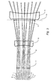
- FIG. 2 shows an enlarged detail "A" from FIG. 1 with this first homogenization stage of the lighting, which is described in more detail below.
- the first microlens array 5 can be a refractive or diffractive microlens array or a combination of two or more such arrays.
- the individual microlenses can have, for example, a hexagonal or a square contour.
- the microlenses can each be designed as collecting or diverging lenses. It is also conceivable to arrange two microlens arrays, each with cylindrical microlenses, in a crossed orientation to one another. For reasons of clarity of the drawing, only three microlenses I, II and III are shown of the first microlens array 5. This is therefore only a schematic reduction to three microlenses, while the actually arranged microlens array has a large number of microlenses. As with known microlens arrays, the individual microlenses are also the same in the first microlens array arrangement 5 used here.
- Each microlens I, II and III generates a conical beam 7 with an aperture angle 8, which is referred to below as the divergence angle or as divergence for short.
- This divergence is selected such that the beam 7 emanating from each microlens I, II and III completely illuminates the condenser pupil 9 in the condenser pupil plane 10 of the condenser 11.
- the position of the condenser pupil plane 10 with the condenser pupil 9 is shown in FIG. 3 , which shows an enlarged detail "B" of FIG. 1 . It can be seen from this that, in the embodiment of the condenser 11 used here, the condenser pupil plane 10 lies between the first condenser lens 12 and the second condenser lens 13. 2 and 3, the rays emanating from the microlenses I, II and III of the first microlens array arrangement 5 and drawn by way of example are also designated I, II and III.
- the divergence of the beams 7 is determined by the refractive power of the individual microlenses I, II and III.
- the refractive power of the individual microlenses and thus the divergence is chosen such that the distance from the condenser-side focal plane 14 of the first microlens array arrangement 5 to Condenser pupil 9 multiplied by the tangent of half the divergence angle 8 ⁇ the radius 13 of the condenser pupil 9.
- the individual convergent or divergent beam bundles 7 emanating from the individual microlenses I, II and III would all have the same aperture angle 8, i.e. the same divergence, but with a different lateral offset in the condenser pupil plane 10 arrive. This offset would lead to portions of the beam bundles 7 striking outside the condenser pupil 9. This would lead to a loss of light intensity and a decrease in brightness at the edge of the condenser pupil 9.
- the first optical auxiliary element 6 In order to prevent this, by means of the first optical auxiliary element 6, all of the beams 7 emanating from the microlenses I, II and III are aligned with the condenser pupil 9.
- a first optical auxiliary element 6 with a positive refractive power is used.
- the focal length of the first optical auxiliary element 6 is substantially equal to the distance of the first optical auxiliary element 6 from the condenser pupil 9. This has the effect that the center rays of the beam bundles 7 emanating from the individual microlenses I, II and III come in front of the first optical one Auxiliary element 6 still run in parallel, are now converging after the first optical auxiliary element 6 in the center of the condenser pupil 9.
- the condenser pupil 9 is slightly over-operated.
- FIG. 3 shows the condenser pupil 9 only filled out, not over-operated, since much more rays would have to be represented for this purpose.
- the large number of microlenses leads to an intensity averaging and thus to a homogenization of the intensity distribution in the condenser pupil 9.
- the condenser-side focal plane 14 that is to say the focus plane, of the individual microlenses of the first microlens array arrangement 5
- intermediate images of the luminous plasma are produced the gas discharge lamp, i.e. the Light source 2.
- the number of these intermediate images corresponds to the number of microlenses I, II and III.
- the second optical auxiliary element 16 has the effect that the center beams of the divergent beam bundles emanating from the individual intermediate images (located in the focal plane 14) are aligned.
- the center beams of these individual beam bundles run divergently and are aligned by the second optical auxiliary element 16 parallel to the optical axis 18 (shown in FIGS. 2 and 3 ) of the overall system.
- the second microlens array arrangement 17 is aligned such that a beam of rays emanating from an intermediate image strikes a microlens of the second microlens array arrangement 17.
- the divergence of the individual microlenses of the second microlens array arrangement 17 determines how large the homogeneous field illuminated on the object 19 is. This clearly means: A small opening angle of the individual beam bundles incident in the condenser pupil plane 10 causes a small, homogeneously illuminated field on the object 19, the structures 20 of which are to be measured. Analogously, a large aperture angle, that is to say a large divergence, of the individual beam bundles incident in the condenser pupil plane 10 produces a large, homogeneously illuminated field on the object 19 to be measured, but with a lower intensity than in the small field.
- the size of the illuminated object field is therefore determined by a suitable choice of the focal lengths of the microlenses of the second microlens array arrangement 17.
- the one with the second multiple auxiliary element 16 and the second microlens array arrangement 17 achieved second multiple image effects the field homogenization of the light intensity.
- the intensity distribution shown in FIG. 4 in the condenser pupil 9 is thereby obtained .
- the condenser pupil 9 is slightly over-operated.
- the divergence of the second microlens array arrangement 17 and the focal length of the condenser 11 determine the size of the illuminated field on the object 19.
- the divergence of the second microlens array arrangement 17, i.e. of the microlenses of this second microlens array arrangement 17, chosen so that the object field to be illuminated is slightly outshone.
- the object 19 is a transparent substrate, on the surface shown on the right, the structures 20 to be examined are applied.
- This object can, for example, be a mask for semiconductor production.
- the optical examination is therefore carried out in transmitted light.
- the structures 20 to be examined are in focus.
- Imaging optics 21 images the structures of the object 19 onto an image recording device 22, which can be a camera, for example.
- the recorded images of the image recording device 22 are transmitted to an image evaluation device 23, which determines the structure widths of the structures 20 from the images.
- the image evaluation device 23 can comprise, for example, a computer with the associated software.
Landscapes
- Physics & Mathematics (AREA)
- General Physics & Mathematics (AREA)
- Length Measuring Devices By Optical Means (AREA)
- Photometry And Measurement Of Optical Pulse Characteristics (AREA)
- Microscoopes, Condenser (AREA)
Applications Claiming Priority (2)
| Application Number | Priority Date | Filing Date | Title |
|---|---|---|---|
| DE10245473 | 2002-09-28 | ||
| DE10245473A DE10245473A1 (de) | 2002-09-28 | 2002-09-28 | Strukturbreiten-Messgerät |
Publications (2)
| Publication Number | Publication Date |
|---|---|
| EP1403676A1 true EP1403676A1 (fr) | 2004-03-31 |
| EP1403676B1 EP1403676B1 (fr) | 2006-05-03 |
Family
ID=31969709
Family Applications (1)
| Application Number | Title | Priority Date | Filing Date |
|---|---|---|---|
| EP03021531A Expired - Lifetime EP1403676B1 (fr) | 2002-09-28 | 2003-09-24 | Appareil de mesure de largeurs de structure |
Country Status (4)
| Country | Link |
|---|---|
| US (1) | US6943901B2 (fr) |
| EP (1) | EP1403676B1 (fr) |
| JP (1) | JP2004117365A (fr) |
| DE (2) | DE10245473A1 (fr) |
Cited By (1)
| Publication number | Priority date | Publication date | Assignee | Title |
|---|---|---|---|---|
| CN113251949A (zh) * | 2021-06-18 | 2021-08-13 | 三代光学科技(天津)有限公司 | 一种微透镜阵列面形的单点光学测量路径生成方法 |
Citations (4)
| Publication number | Priority date | Publication date | Assignee | Title |
|---|---|---|---|---|
| JPH0560982A (ja) * | 1991-08-30 | 1993-03-12 | Nikon Corp | ケーラー照明光学系 |
| DE10062579A1 (de) * | 1999-12-15 | 2001-06-21 | Nikon Corp | Optischer Integrierer,optische Beleuchtungseinrichtung, Photolithographie-Belichtungseinrichtung,und Beobachtungseinrichtung |
| US20020001090A1 (en) * | 2000-06-29 | 2002-01-03 | Leica Microsystems Wetzlar Gmbh. | Illumination device; and coordinate measuring instrument having an illumination device |
| JP2002023061A (ja) * | 2000-07-11 | 2002-01-23 | Nikon Corp | 顕微鏡の暗視野照明装置および暗視野照明方法 |
Family Cites Families (7)
| Publication number | Priority date | Publication date | Assignee | Title |
|---|---|---|---|---|
| US5359440A (en) * | 1989-10-23 | 1994-10-25 | Sharp Kabushiki Kaisha | Image display apparatus with microlens plate having mutually fused together lenses resulting in hexagonal shaped microlenses |
| WO1995034800A1 (fr) * | 1994-06-14 | 1995-12-21 | Visionix Ltd. | Appareil de mappage d'elements optiques |
| US5473408A (en) * | 1994-07-01 | 1995-12-05 | Anvik Corporation | High-efficiency, energy-recycling exposure system |
| TW374864B (en) * | 1994-10-28 | 1999-11-21 | Toshiba Corp | Projecting type displaying device and photo-modulating elements array used therein |
| JPH1164787A (ja) * | 1997-08-21 | 1999-03-05 | Seiko Epson Corp | 投写型表示装置 |
| JPH11174372A (ja) * | 1997-12-11 | 1999-07-02 | Victor Co Of Japan Ltd | 投影装置の照明装置及び投影装置 |
| US6731383B2 (en) * | 2000-09-12 | 2004-05-04 | August Technology Corp. | Confocal 3D inspection system and process |
-
2002
- 2002-09-28 DE DE10245473A patent/DE10245473A1/de not_active Withdrawn
-
2003
- 2003-09-24 EP EP03021531A patent/EP1403676B1/fr not_active Expired - Lifetime
- 2003-09-24 DE DE50303167T patent/DE50303167D1/de not_active Expired - Lifetime
- 2003-09-26 US US10/672,048 patent/US6943901B2/en not_active Expired - Fee Related
- 2003-09-29 JP JP2003338380A patent/JP2004117365A/ja active Pending
Patent Citations (4)
| Publication number | Priority date | Publication date | Assignee | Title |
|---|---|---|---|---|
| JPH0560982A (ja) * | 1991-08-30 | 1993-03-12 | Nikon Corp | ケーラー照明光学系 |
| DE10062579A1 (de) * | 1999-12-15 | 2001-06-21 | Nikon Corp | Optischer Integrierer,optische Beleuchtungseinrichtung, Photolithographie-Belichtungseinrichtung,und Beobachtungseinrichtung |
| US20020001090A1 (en) * | 2000-06-29 | 2002-01-03 | Leica Microsystems Wetzlar Gmbh. | Illumination device; and coordinate measuring instrument having an illumination device |
| JP2002023061A (ja) * | 2000-07-11 | 2002-01-23 | Nikon Corp | 顕微鏡の暗視野照明装置および暗視野照明方法 |
Non-Patent Citations (2)
| Title |
|---|
| PATENT ABSTRACTS OF JAPAN vol. 017, no. 372 (P - 1573) 13 July 1993 (1993-07-13) * |
| PATENT ABSTRACTS OF JAPAN vol. 2002, no. 05 3 May 2002 (2002-05-03) * |
Cited By (2)
| Publication number | Priority date | Publication date | Assignee | Title |
|---|---|---|---|---|
| CN113251949A (zh) * | 2021-06-18 | 2021-08-13 | 三代光学科技(天津)有限公司 | 一种微透镜阵列面形的单点光学测量路径生成方法 |
| CN113251949B (zh) * | 2021-06-18 | 2021-11-30 | 三代光学科技(天津)有限公司 | 一种微透镜阵列面形的单点光学测量路径生成方法 |
Also Published As
| Publication number | Publication date |
|---|---|
| US20040070821A1 (en) | 2004-04-15 |
| US6943901B2 (en) | 2005-09-13 |
| JP2004117365A (ja) | 2004-04-15 |
| EP1403676B1 (fr) | 2006-05-03 |
| DE50303167D1 (de) | 2006-06-08 |
| DE10245473A1 (de) | 2004-04-08 |
Similar Documents
| Publication | Publication Date | Title |
|---|---|---|
| DE69526890T2 (de) | Ausseraxiales Ausrichtsystem für abtastende Photolithographie | |
| DE69728572T2 (de) | Mikroabbildungssystem | |
| DE69326630T2 (de) | Beleuchtungsvorrichtung für einen Projektionsbelichtungsapparat | |
| DE3843876C2 (fr) | ||
| DE102018130901A1 (de) | Optische Messeinrichtung | |
| DE112015000627B4 (de) | Mikrospektroskopische Vorrichtung | |
| DE10109929A1 (de) | Vorrichtung zur Wellenfronterfassung | |
| EP3781899B1 (fr) | Dispositif optique de mesure et procédé de mesure d'un élément optique | |
| WO2003096356A2 (fr) | Microscope aux rayons x reflechissant et systeme de controle concus pour examiner des objets presentant des longueurs d'onde ≤ 100nm | |
| DE102008003916A1 (de) | Projektionsbelichtungsanlage für die Mikrolithographie mit Messvorrichtung sowie Verfahren zum Messen einer Bestrahlungsstärkeverteilung | |
| DE102008040742A1 (de) | Verfahren und Vorrichtung zur Überwachung von Mehrfachspiegelanordnungen, optische Anordnung mit einer derartigen Vorrichtung sowie mit einer zweiten Mehrfachspiegelanordnung zum Ein- und Ausschalten einer ersten Mehrfachspiegelanordnung sowie Beleuchtungsoptik für eine Projektionsbelichtungsanlage mit einer derartigen Vorrichtung | |
| DE19639939A1 (de) | Optische Spektralmeßvorrichtung | |
| DE102019208552A1 (de) | Verfahren zum Ermitteln eines Produktions-Luftbildes eines zu vermessenden Objektes | |
| DE102012204674B4 (de) | Strahlregelungsvorrichtung für einen EUV-Beleuchtungsstrahl | |
| DE102011005826A1 (de) | Optische Vorrichtung | |
| DE102006036504A1 (de) | Vorrichtung und Verfahren zur Messung des Höhenprofils eines strukturierten Substrats | |
| EP3139147A1 (fr) | Dispositif et procede de mesure d'une grandeur nominale optique dependant de la longueur d'onde d'un systeme optique | |
| DE102019215972A1 (de) | Verfahren zur Messung einer Reflektivität eines Objekts für Messlicht sowie Metrologiesystem zur Durchführung des Verfahrens | |
| DE102021204170B4 (de) | Messvorrichtung sowie Verfahren zur Messung einer Wirkung einer wellenlängenabhängigen Messlicht-Reflektivität sowie einer Wirkung einer Polarisation von Messlicht auf eine Messlicht-Beaufschlagung einer Lithografiemaske | |
| DE102024203350B4 (de) | Energie-Detektions-Baugruppe für ein Beleuchtungssystem eines Maskeninspektionssystems zum Einsatz mit EUV-Beleuchtungslicht | |
| EP1403676B1 (fr) | Appareil de mesure de largeurs de structure | |
| DE102013224583A1 (de) | Messanordnung zur Verwendung bei der Trajektorienbestimmung fliegender Objekte | |
| DE102012211846A1 (de) | Verfahren zum Messen einer winkelaufgelösten Intensitätsverteilung sowie Projektionsbelichtungsanlage | |
| DE102023205077B4 (de) | Verfahren und Vorrichtung zur Bestimmung einer objektabhängigen Fokusablage, Verfahren zur Vermessung eines Objekts und Koordinatenmessgerät | |
| DE10146945A1 (de) | Meßanordnung und Meßverfahren |
Legal Events
| Date | Code | Title | Description |
|---|---|---|---|
| PUAI | Public reference made under article 153(3) epc to a published international application that has entered the european phase |
Free format text: ORIGINAL CODE: 0009012 |
|
| AK | Designated contracting states |
Kind code of ref document: A1 Designated state(s): AT BE BG CH CY CZ DE DK EE ES FI FR GB GR HU IE IT LI LU MC NL PT RO SE SI SK TR |
|
| AX | Request for extension of the european patent |
Extension state: AL LT LV MK |
|
| 17P | Request for examination filed |
Effective date: 20040820 |
|
| 17Q | First examination report despatched |
Effective date: 20041001 |
|
| AKX | Designation fees paid |
Designated state(s): DE FR GB |
|
| GRAP | Despatch of communication of intention to grant a patent |
Free format text: ORIGINAL CODE: EPIDOSNIGR1 |
|
| GRAS | Grant fee paid |
Free format text: ORIGINAL CODE: EPIDOSNIGR3 |
|
| GRAA | (expected) grant |
Free format text: ORIGINAL CODE: 0009210 |
|
| AK | Designated contracting states |
Kind code of ref document: B1 Designated state(s): DE FR GB |
|
| REG | Reference to a national code |
Ref country code: GB Ref legal event code: FG4D Free format text: NOT ENGLISH |
|
| REF | Corresponds to: |
Ref document number: 50303167 Country of ref document: DE Date of ref document: 20060608 Kind code of ref document: P |
|
| GBT | Gb: translation of ep patent filed (gb section 77(6)(a)/1977) |
Effective date: 20060712 |
|
| ET | Fr: translation filed | ||
| PLBE | No opposition filed within time limit |
Free format text: ORIGINAL CODE: 0009261 |
|
| STAA | Information on the status of an ep patent application or granted ep patent |
Free format text: STATUS: NO OPPOSITION FILED WITHIN TIME LIMIT |
|
| 26N | No opposition filed |
Effective date: 20070206 |
|
| PGFP | Annual fee paid to national office [announced via postgrant information from national office to epo] |
Ref country code: DE Payment date: 20100922 Year of fee payment: 8 |
|
| PGFP | Annual fee paid to national office [announced via postgrant information from national office to epo] |
Ref country code: FR Payment date: 20111005 Year of fee payment: 9 Ref country code: GB Payment date: 20110926 Year of fee payment: 9 |
|
| GBPC | Gb: european patent ceased through non-payment of renewal fee |
Effective date: 20120924 |
|
| REG | Reference to a national code |
Ref country code: FR Ref legal event code: ST Effective date: 20130531 |
|
| PG25 | Lapsed in a contracting state [announced via postgrant information from national office to epo] |
Ref country code: DE Free format text: LAPSE BECAUSE OF NON-PAYMENT OF DUE FEES Effective date: 20130403 Ref country code: GB Free format text: LAPSE BECAUSE OF NON-PAYMENT OF DUE FEES Effective date: 20120924 |
|
| REG | Reference to a national code |
Ref country code: DE Ref legal event code: R119 Ref document number: 50303167 Country of ref document: DE Effective date: 20130403 |
|
| PG25 | Lapsed in a contracting state [announced via postgrant information from national office to epo] |
Ref country code: FR Free format text: LAPSE BECAUSE OF NON-PAYMENT OF DUE FEES Effective date: 20121001 |
|
| P01 | Opt-out of the competence of the unified patent court (upc) registered |
Effective date: 20230525 |