EP1403762A2 - SIMD Befehle ausführender Prozessor - Google Patents
SIMD Befehle ausführender Prozessor Download PDFInfo
- Publication number
- EP1403762A2 EP1403762A2 EP20030020559 EP03020559A EP1403762A2 EP 1403762 A2 EP1403762 A2 EP 1403762A2 EP 20030020559 EP20030020559 EP 20030020559 EP 03020559 A EP03020559 A EP 03020559A EP 1403762 A2 EP1403762 A2 EP 1403762A2
- Authority
- EP
- European Patent Office
- Prior art keywords
- instruction
- data
- register
- simd
- execution unit
- Prior art date
- Legal status (The legal status is an assumption and is not a legal conclusion. Google has not performed a legal analysis and makes no representation as to the accuracy of the status listed.)
- Withdrawn
Links
Images


























Classifications
-
- G—PHYSICS
- G06—COMPUTING OR CALCULATING; COUNTING
- G06F—ELECTRIC DIGITAL DATA PROCESSING
- G06F9/00—Arrangements for program control, e.g. control units
- G06F9/06—Arrangements for program control, e.g. control units using stored programs, i.e. using an internal store of processing equipment to receive or retain programs
- G06F9/30—Arrangements for executing machine instructions, e.g. instruction decode
- G06F9/30003—Arrangements for executing specific machine instructions
- G06F9/30007—Arrangements for executing specific machine instructions to perform operations on data operands
- G06F9/3001—Arithmetic instructions
- G06F9/30014—Arithmetic instructions with variable precision
-
- G—PHYSICS
- G06—COMPUTING OR CALCULATING; COUNTING
- G06F—ELECTRIC DIGITAL DATA PROCESSING
- G06F9/00—Arrangements for program control, e.g. control units
- G06F9/06—Arrangements for program control, e.g. control units using stored programs, i.e. using an internal store of processing equipment to receive or retain programs
- G06F9/30—Arrangements for executing machine instructions, e.g. instruction decode
- G06F9/30003—Arrangements for executing specific machine instructions
- G06F9/30007—Arrangements for executing specific machine instructions to perform operations on data operands
- G06F9/30021—Compare instructions, e.g. Greater-Than, Equal-To, MINMAX
-
- G—PHYSICS
- G06—COMPUTING OR CALCULATING; COUNTING
- G06F—ELECTRIC DIGITAL DATA PROCESSING
- G06F9/00—Arrangements for program control, e.g. control units
- G06F9/06—Arrangements for program control, e.g. control units using stored programs, i.e. using an internal store of processing equipment to receive or retain programs
- G06F9/30—Arrangements for executing machine instructions, e.g. instruction decode
- G06F9/30003—Arrangements for executing specific machine instructions
- G06F9/30007—Arrangements for executing specific machine instructions to perform operations on data operands
- G06F9/30025—Format conversion instructions, e.g. Floating-Point to Integer, decimal conversion
-
- G—PHYSICS
- G06—COMPUTING OR CALCULATING; COUNTING
- G06F—ELECTRIC DIGITAL DATA PROCESSING
- G06F9/00—Arrangements for program control, e.g. control units
- G06F9/06—Arrangements for program control, e.g. control units using stored programs, i.e. using an internal store of processing equipment to receive or retain programs
- G06F9/30—Arrangements for executing machine instructions, e.g. instruction decode
- G06F9/30003—Arrangements for executing specific machine instructions
- G06F9/30007—Arrangements for executing specific machine instructions to perform operations on data operands
- G06F9/30036—Instructions to perform operations on packed data, e.g. vector, tile or matrix operations
-
- G—PHYSICS
- G06—COMPUTING OR CALCULATING; COUNTING
- G06F—ELECTRIC DIGITAL DATA PROCESSING
- G06F9/00—Arrangements for program control, e.g. control units
- G06F9/06—Arrangements for program control, e.g. control units using stored programs, i.e. using an internal store of processing equipment to receive or retain programs
- G06F9/30—Arrangements for executing machine instructions, e.g. instruction decode
- G06F9/30003—Arrangements for executing specific machine instructions
- G06F9/30007—Arrangements for executing specific machine instructions to perform operations on data operands
- G06F9/30036—Instructions to perform operations on packed data, e.g. vector, tile or matrix operations
- G06F9/30038—Instructions to perform operations on packed data, e.g. vector, tile or matrix operations using a mask
-
- G—PHYSICS
- G06—COMPUTING OR CALCULATING; COUNTING
- G06F—ELECTRIC DIGITAL DATA PROCESSING
- G06F9/00—Arrangements for program control, e.g. control units
- G06F9/06—Arrangements for program control, e.g. control units using stored programs, i.e. using an internal store of processing equipment to receive or retain programs
- G06F9/30—Arrangements for executing machine instructions, e.g. instruction decode
- G06F9/30094—Condition code generation, e.g. Carry, Zero flag
-
- G—PHYSICS
- G06—COMPUTING OR CALCULATING; COUNTING
- G06F—ELECTRIC DIGITAL DATA PROCESSING
- G06F9/00—Arrangements for program control, e.g. control units
- G06F9/06—Arrangements for program control, e.g. control units using stored programs, i.e. using an internal store of processing equipment to receive or retain programs
- G06F9/30—Arrangements for executing machine instructions, e.g. instruction decode
- G06F9/30145—Instruction analysis, e.g. decoding, instruction word fields
-
- G—PHYSICS
- G06—COMPUTING OR CALCULATING; COUNTING
- G06F—ELECTRIC DIGITAL DATA PROCESSING
- G06F9/00—Arrangements for program control, e.g. control units
- G06F9/06—Arrangements for program control, e.g. control units using stored programs, i.e. using an internal store of processing equipment to receive or retain programs
- G06F9/30—Arrangements for executing machine instructions, e.g. instruction decode
- G06F9/30145—Instruction analysis, e.g. decoding, instruction word fields
- G06F9/3016—Decoding the operand specifier, e.g. specifier format
-
- G—PHYSICS
- G06—COMPUTING OR CALCULATING; COUNTING
- G06F—ELECTRIC DIGITAL DATA PROCESSING
- G06F9/00—Arrangements for program control, e.g. control units
- G06F9/06—Arrangements for program control, e.g. control units using stored programs, i.e. using an internal store of processing equipment to receive or retain programs
- G06F9/30—Arrangements for executing machine instructions, e.g. instruction decode
- G06F9/30145—Instruction analysis, e.g. decoding, instruction word fields
- G06F9/3016—Decoding the operand specifier, e.g. specifier format
- G06F9/30167—Decoding the operand specifier, e.g. specifier format of immediate specifier, e.g. constants
-
- G—PHYSICS
- G06—COMPUTING OR CALCULATING; COUNTING
- G06F—ELECTRIC DIGITAL DATA PROCESSING
- G06F9/00—Arrangements for program control, e.g. control units
- G06F9/06—Arrangements for program control, e.g. control units using stored programs, i.e. using an internal store of processing equipment to receive or retain programs
- G06F9/30—Arrangements for executing machine instructions, e.g. instruction decode
- G06F9/38—Concurrent instruction execution, e.g. pipeline or look ahead
-
- G—PHYSICS
- G06—COMPUTING OR CALCULATING; COUNTING
- G06F—ELECTRIC DIGITAL DATA PROCESSING
- G06F9/00—Arrangements for program control, e.g. control units
- G06F9/06—Arrangements for program control, e.g. control units using stored programs, i.e. using an internal store of processing equipment to receive or retain programs
- G06F9/30—Arrangements for executing machine instructions, e.g. instruction decode
- G06F9/38—Concurrent instruction execution, e.g. pipeline or look ahead
- G06F9/3885—Concurrent instruction execution, e.g. pipeline or look ahead using a plurality of independent parallel functional units
- G06F9/3887—Concurrent instruction execution, e.g. pipeline or look ahead using a plurality of independent parallel functional units controlled by a single instruction for multiple data lanes [SIMD]
Definitions
- the present invention relates to a processor such as DSP and CPU, and more particularly to a processor suitable for performing signal processing for sounds, images and others.
- processors are increasingly required to be capable of high-speed media processing represented by sound and image signal processing.
- processors responding to such requirement, there exist Pentium (R)/ Pentium (R) III/ Pentium 4 (R) MMX/SSE/SSE2 and others produced by the Intel Corporation of the United States supporting SIMD (Single Instruction Multiple Data) instructions.
- MMX for example, is capable of performing the same operations in one instruction on maximum of eight integers stored in a 64-bit MMX register.
- an existing processor is capable of comparing two data elements stored in 32-bit registers on a byte-by-byte basis, and setting comparison results to four flags.
- the processor needs to read out all four flags and execute more than one instruction for judging whether all such values are zero or not. This requires a plurality of instructions for evaluating results every time a comparison is made against another set of pixel values when four pixel values are used as a unit of comparison, resulting in an increased number of instructions and therefore a decreased speed of image processing.
- the present invention has been conceived in view of the above problem, and it is an object of this invention to provide a processor capable of executing sophisticated SIMD operations and a processor capable of high-speed digital signal processing suited for multimedia purposes.
- t he processor is capable of executing a characteristic SIMD instruction for judging whether or not results of operations performed under a SIMD compare instruction are all zero and setting such results to condition flags. This allows a faster extraction of results of SIMD compare instructions (especially, agreement/disagreement of results), as well as a faster comparison processing to be performed on more than one pixel value as a processing unit and a faster detection of the EOF (End Of File) of a file.
- EOF End Of File
- the processor according to the present invention is capable of executing a characteristic instruction for storing, into a memory and the like, two pieces of byte data stored in one register (byte data stored in the higher 16 bits and byte data stored in the lower 16 bits). This eliminates the need for data type conversions when byte data is handled in 16-bit SIMD, making a speed of processing faster.
- the processor according to the present invention is capable of executing a characteristic instruction for storing an immediate value into the higher 16 bits of a register without changing the lower 16 bits of the register.
- This instruction when combined with Instruction "mov Rb, I16", makes it possible for a 32-bit immediate value to be set in a register.
- the processor according to the present invention is capable of executing a characteristic instruction for making a switch of objects to be added, depending on the value of a vector condition flag. This makes it possible for a single program to support half-pel motion compensation (motion compensation performed on a per-half-pixel basis) regardless of whether pixels are integer pixels or half pixels.
- the processor according to the present invention is capable of executing a characteristic instruction for generating a value depending on the sign (positive/negative) of the value held in a register and whether a value held in a register is zero or not. This makes inverse quantization faster in image processing, since 1 is outputted when a certain value is positive, -1 when negative, and 0 when 0.
- the processor according to the present invention is capable of executing a characteristic instruction for aligning word data and extracting different word data depending on a vector condition flag.
- This instruction makes it possible for a single program to support half-pel motion compensation (motion compensation performed on a per-half-pixel basis) regardless of whether pixels are integer pixels or half pixels.
- the processor according to the present invention is capable of executing a characteristic instruction for adding two values and further adding 1 when one of the two values is positive. This realizes a faster rounding of an absolute value in image processing.
- the processor according to the present invention is capable of executing a characteristic instruction for moving values held in arbitrary two registers to two consecutive registers. Since values held in independent two registers are moved in one cycle. under this instruction, an effect of reducing the number of cycles in a loop can be achieved. Also, this instruction, which does not involve register renaming (destruction of a register value), is effective when data is moved between loop generations (iterations).
- the processor according to the present invention is capable of executing a characteristic instruction for performing branches and setting condition flags (predicates, here) in a loop. This makes faster a loop to be executed by means of PROLOG/EPILOG removal software pipelining.
- the processor according to the present invention is capable of executing a characteristic instruction for determining a sum of absolute value differences. This makes faster the speed of summing up absolute value differences in motion prediction as part of image processing.
- the processor according to the present invention is capable of executing a characteristic instruction for converting a signed value into a saturated signed value at an arbitrary position (digit). This facilitates programming since there is no need for setting a position where saturation is performed to a specific position at the time of assembler programming.
- the processor according to the present invention is capable of executing a characteristic instruction for selecting one of the values held in two registers on a word-by-word basis. This allows word data to be stored at an arbitrary position in a register, and therefore makes faster repetitions of data reshuffling. Moreover, this instruction has an effect of increasing the flexibility of SIMD operations.
- the processor according to the present invention is capable of executing a characteristic instruction for extending results of a SIMD operation. This allows processing for making data size all the same by performing sign extension or zero extension to be performed in one cycle, after performing the SIMD operations.
- the processor according to the present invention is capable of executing a characteristic instruction for executing SIMD operations specified by condition flags and the like. This makes it possible for a single program to perform such dynamic processing as one in which the types of operations to be performed are determined depending on results of other processing.
- the processor according to the present invention is extremely useful in the present age in which the advent of high-performance and cost effective multimedia apparatuses is desired.
- the processor of the present invention is a general-purpose processor which has been developed targeting at the field of AV media signal processing technology, and instructions issued in this processor offer a higher degree of parallelism than ordinary microcomputers. Used as a core common to mobile phones, mobile AV devices, digital televisions, DVDs and others, the processor can improve software usability. Furthermore, the present processor allows multiple high-performance media processes to be performed with high cost effectiveness, and provides a development environment for high-level languages intended for improving development efficiency.
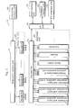
- Fig.1 is a schematic block diagram showing the present processor.
- the processor 1 is comprised of an instruction control unit 10, a decoding unit 20, a register file 30, an operation unit 40, an I/F unit 50, an instruction memory unit 60, a data memory unit 70, an extended register unit 80, and an I/O interface unit 90.
- the operation unit 40 includes arithmetic and logic/comparison operation units 41 ⁇ 43, a multiplication/sum of products operation unit 44, a barrel shifter 45, a divider 46, and a converter 47 for performing SIMD instructions.
- the multiplication/sum of products operation unit 44 is capable of handling maximum of 65-bit accumulation so as not to decrease bit precision.
- the multiplication/sum of products operation unit 44 is also capable of executing SIMD instructions as in the case of the arithmetic and logic/comparison operation units 41 ⁇ 43. Furthermore, the processor 1 is capable of parallel execution of an arithmetic and logic/comparison operation instruction on maximum of three data elements.
- Fig.2 is a schematic diagram showing the arithmetic and logic/comparison operation units 41 ⁇ 43.
- Each of the arithmetic and logic/comparison operation units 41 ⁇ 43 is made up of an ALU unit 41a, a saturation processing unit 41b, and a flag unit 41c.
- the ALU unit 41a includes an arithmetic operation unit, a logical operation unit, a comparator, and a TST.
- the bit widths of operation data to be supported are 8 bits (use four operation units in parallel), 16 bits (use two operation units in parallel) and 32 bits (process 32-bit data using all operation units).
- the flag unit 41c and the like detects an overflow and generates a condition flag.
- the comparator and the TST an arithmetic shift right, saturation by the saturation processing unit 41b, the detection of maximum/minimum values, absolute value generation processing are performed.
- Fig.3 is a block diagram showing the configuration of the barrel shifter 45.
- the barrel shifter 45 which is made up of selectors 45a and 45b, a higher bit shifter 45c, a lower bit shifter 45d, and a saturation processing unit 45e, executes an arithmetic shift of data (shift in the 2's complement number system) or a logical shift of data (unsigned shift).
- arithmetic shift of data shift in the 2's complement number system
- a logical shift of data unsigned shift.
- 32-bit or 64-bit data are inputted to and outputted from the barrel shifter 45.
- the amount of shift of target data stored in the registers 30a and 30b are specified by another register or according to its immediate value.
- An arithmetic or logical shift in the range of left 63 bits and right 63 bits is performed for the data, which is then outputted in an input bit length.
- the barrel shifter 45 is capable of shifting 8-, 16-, 32-, and 64-bit data in response to a SIMD instruction.
- the barrel shifter 45 can shift four pieces of 8-bit data in parallel.
- Arithmetic shift which is a shift in the 2's complement number system, is performed for aligning decimal points at the time of addition and subtraction, for multiplying a power of 2 (2, the 2 nd power of 2, the -1 st power of 2) and other purposes.
- Fig.4 is a block diagram showing the configuration of the converter 47.
- the converter 47 is made up of a saturation block (SAT) 47a, a BSEQ block 47b, an MSKGEN block 47c, a VSUMB block 47d, a BCNT block 47e, and an IL block 47f.
- SAT saturation block
- the saturation block (SAT) 47a performs saturation processing for input data. Having two blocks for the saturation processing of 32-bit data makes it possible to support a SIMD instruction executed for two data elements in parallel.
- the BSEQ block 47b counts consecutive 0s or 1s from the MSB.
- the MSKGEN block 47c outputs a specified bit segment as 1, while outputting the others as 0.
- the VSUMB block 47d divides the input data into specified bit widths, and outputs their total sum.
- the BCNT block 47e counts the number of bits in the input data specified as 1.
- the IL block 47f divides the input data into specified bit widths, and outputs a value resulted from exchanging the position of each data block.
- Fig.5 is a block diagram showing the configuration of the divider 46. Letting a dividend be 64 bits and a divisor be 32 bits, the divider 46 outputs 32 bits as a quotient and a modulo, respectively. 34 cycles are involved for obtaining a quotient and a modulo.
- the divider 46 can handle both singed and unsigned data. Note, however, that an identical setting is made concerning the presence/absence of signs of data serving as a dividend and a divisor. Also, the divider 46 has the capability of outputting an overflow flag, and a 0 division flag.
- Fig.6 is a block diagram showing the configuration of the multiplication/sum of products operation unit 44.
- the multiplication/sum of products operation unit 44 which is made up of two 32-bit multipliers (MUL) 44a and 44b, three 64-bit adders (Adder) 44c ⁇ 44e, a selector 44f and a saturation processing unit (Saturation) 44g, performs the following multiplications and sums of products:
- Fig.7 is a block diagram showing the configuration of the instruction control unit 10.
- the instruction control unit 10 which is made up of an instruction cache 10a, an address management unit 10b, instruction buffers 10c ⁇ 10e, a jump buffer 10f, and a rotation unit (rotation) 10g, issues instructions at ordinary times and at branch points. Having three 128-bit instruction buffers (the instruction buffers 10c ⁇ 10e) makes it possible to support the maximum number of parallel instruction execution.
- the instruction control unit 10 stores in advance a branch target instruction into the jump buffer 10f and stores a branch target address into the below-described TAR register before performing a branch (settar instruction).
- the instruction control unit 10 performs the branch using the branch target address stored in the TAR register and the branch target instruction stored in the jump buffer 10f.
- the processor 1 is a processor employing the VLIW architecture.
- the VLIW architecture is an architecture allowing a plurality of instructions (e.g. load, store, operation, and branch) to be stored in a single instruction word, and such instructions to be executed all at once.
- programmers describing a set of instructions which can be executed in parallel as a single issue group it is possible for such issue group to be processed in parallel.
- the delimiter of an issue group is indicated by ";;”. Notational examples are described below.
- the instruction control unit 10 identifies an issue group and sends it to the decoding unit 20.
- the decoding unit 20 decodes the instructions in the issue group, and controls resources required for executing such instructions.
- Register name Bit width No. of registers Usage R0 ⁇ R31 32 bits 32 General-purpose registers. Used as data memory pointer, data storage and the like when operation instruction is executed.
- TAR 32 bits 1 Branch register. Used as branch address storage at branch point.
- LR 32 bits 1 Link register.
- SVR 16 bits 2 Save register. Used for saving condition flag (CFR) and various modes.
- M0 ⁇ M1 (MH0:ML0 ⁇ MH1 ⁇ ML1) 64 bits 2 Operation registers. Used as data storage when operation instruction is executed.
- Table 2 below lists a set of flags (flags managed in a condition flag register and the like described later) of the processor 1.
- Flag name Bit width No. of flags Usage C0 ⁇ C7 1 8 Condition flags. Indicate if condition is established or not. VC0 ⁇ VC3 1 4 Condition flags for media processing extension instruction. Indicate if condition is established or not. OVS 1 1 Overflow flag. Detects overflow at the time of operation. CAS 1 1 Carry flag. Detects carry at the time of operation. BPO 5 1 Specifies bit position. Specifies bit positions to be processed when mask processing instruction is executed. ALN 2 1 Specified byte alignment. FXP 1 1 Fixed point operation mode. UDR 32 1 Undefined register.
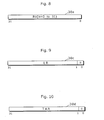
- Fig.8 is a diagram showing the configuration of the general-purpose registers (R0 ⁇ R31) 30a.
- the general-purpose registers (R0 ⁇ R31) 30a are a group of 32-bit registers that constitute an integral part of the context of a task to be executed and that store data or addresses. Note that the general-purpose registers R30 and R31 are used by hardware as a global pointer and a stack pointer, respectively.
- Fig.9 is a diagram showing the configuration of a link register (LR) 30c.
- the processor 1 also has a save register (SVR) not illustrated in the diagram.
- the link register (LR) 30c is a 32-bit register for storing a return address at the time of a function call.
- the save register (SVR) is a 16-bit register for saving a condition flag (CFR.CF) of the condition flag register at the time of a function call.
- the link register (LR) 30c is used also for the purpose of increasing the speed of loops, as in the case of a branch register (TAR) to be explained later. 0 is always read out as the lower 1 bit, but 0 must be written at the time of writing.
- the processor 1 when "call (brl, jmpl)" instructions are executed, the processor 1 saves a return address in the link register (LR) 30c and saves a condition flag (CFR.CF) in the save register (SVR).
- the processor 1 fetches the return address (branch target address) from the link register (LR) 30c, and restores a program counter (PC).
- the processor 1 fetches the branch target address (return address) from the link register (LR) 30c, and stores (restores) it in/to the program counter (PC).
- the processor 1 fetches the condition flag from the save register (SVR) so as to store (restore) it in/to a condition flag area CFR.CF in the condition flag register (CFR) 32.
- Fig.10 is a diagram showing the configuration of the branch register (TAR) 30d.
- the branch register (TAR) 30d is a 32-bit register for storing a branch target address, and used mainly for the purpose of increasing the speed of loops. 0 is always read out as the lower 1 bit, but 0 must be written at the time of writing.
- the processor 1 fetches a branch target address from the branch register (TAR) 30d, and stores it in the program counter (PC).
- PC program counter
- a branch penalty will be 0.
- An increased loop speed can be achieved by storing the top address of a loop in the branch register (TAR) 30d.
- Fig.11 is a diagram showing the configuration of a program status register (PSR) 31.
- the program status register (PSR) 31 which constitutes an integral part of the context of a task to be executed, is a 32-bit register for storing the following processor status information:
- Bit SWE indicates whether the switching of VMP (Virtual Multi-Processor) to LP (Logical Processor) is enabled or disabled. "0" indicates that switching to LP is disabled and “1" indicates that switching to LP is enabled.
- Bit FXP indicates a fixed point mode. "0" indicates the mode 0 and "1" indicates the mode 1.
- Bit IH is an interrupt processing flag indicating that maskable interrupt processing is ongoing or not. "1" indicates that there is an ongoing interrupt processing and "0" indicates that there is no ongoing interrupt processing. This flag is automatically set on the occurrence of an interrupt. This flag is used to make a distinction of whether interrupt processing or program processing is taking place at a point in the program to which the processor returns in response to "rti" instruction.
- Bit LPIE3 indicates whether LP-specific interrupt 3 is enabled or disabled. "1" indicates that an interrupt is enabled and “0" indicates that an interrupt is disabled.
- Bit LPIE2 indicates whether LP-specific interrupt 2 is enabled or disabled. "1" indicates that an interrupt is enabled and "0" indicates that an interrupt is disabled.
- Bit LPIE1 indicates whether LP-specific interrupt 1 is enabled or disabled. “1" indicates that an interrupt is enabled and “0" indicates that an interrupt is disabled.
- Bit LPIEO indicates whether LP-specific interrupt 0 is enabled or disabled. "1" indicates that an interrupt is enabled and "0" indicates that an interrupt is disabled.
- Bit AEE indicates whether a misalignment exception is enabled or disabled. "1" indicates that a misalignment exception is enabled and "0" indicates that a misalignment exception is disabled.
- Bit IE indicates whether a level interrupt is enabled or disabled. "1" indicates that a level interrupt is enabled and “0" indicates a level interrupt is disabled.
- Bit IM [7:0] indicates an interrupt mask, and ranges from levels 0 ⁇ 7, each being able to be masked at its own level.
- Level 0 is the highest level. Of interrupt requests which are not masked by any IMs, only the interrupt request with the highest level is accepted by the processor 1. When an interrupt request is accepted, levels below the accepted level are automatically masked by hardware.
- IM[0] denotes a mask of level 0, IM[1] a mask of level 1, IM[2] a mask of level 2, IM[3] a mask of level 3, IM[4] a mask of level 4, IM[5] a mask of level 5, IM[6] a mask of level 6, and IM[7] a mask of level 7.
- reserved indicates a reserved bit. 0 is always read out. 0 must be written at the time of writing.
- Fig.12 is a diagram showing the configuration of the condition flag register (CFR) 32.
- the condition flag register (CFR) 32 which constitutes an integral part of the context of a task to be executed, is a 32-bit register made up of condition flags, operation flags, vector condition flags, an operation instruction bit position specification field, and a SIMD data alignment information field.
- Bit BPO [4:0] indicates a bit position. It is used in an instruction that requires a bit position specification.
- Bit VC0 ⁇ VC3 are vector condition flags. Starting from a byte on the LSB side or a half word through to the MSB side, each corresponds to a flag ranging from VC0 through to VC3.
- Bit OVS is an overflow flag (summary). It is set on the detection of saturation and overflow. If not detected, a value before the instruction is executed is retained. Clearing of this flag needs to be carried out by software.
- Bit CAS is a carry flag (summary). It is set when a carry occurs under "addc” instruction, or when a borrow occurs under “subc” instruction. If there is no occurrence of a carry under "addc” instruction, or a borrow under “subc” instruction, a value before the instruction is executed is retained. Clearing of this flag needs to be carried out by software.
- Bit C0 ⁇ C7 are condition flags.
- the value of the flag C7 is always 1. A reflection of a FALSE condition (writing of 0) made to the flag C7 is ignored.
- reserved indicates a reserved bit. 0 is always read out. 0 must be written at the time of writing.
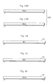
- Figs.13A and 13B are diagrams showing the configurations of accumulators (M0, M1) 30b.
- Such accumulators (M0, M1) 30b which constitute an integral part of the context of a task to be executed, are made up of a 32-bit register MHO-MH1 (register for multiply and divide/sum of products (the higher 32 bits)) shown in Fig.13A and a 32-bit register MLO-ML1 (register for multiply and divide/sum of products (the lower 32 bits)) shown in Fig.13B.
- the register MHO-MH1 is used for storing the higher 32 bits of operation results at the time of a multiply instruction, while used as the higher 32 bits of the accumulators at the time of a sum of products instruction. Moreover, the register MHO-MH1 can be used in combination with the general-purpose registers in the case where a bit stream is handled. Meanwhile, the register MLO-ML1 is used for storing the lower 32 bits of operation results at the time of a multiply instruction, while used as the lower 32 bits of the accumulators at the time of a sum of products instruction.
- Fig.14 is a diagram showing the configuration of a program counter (PC) 33.
- This program counter (PC) 33 which constitutes an integral part of the context of a task to be executed, is a 32-bit counter that holds the address of an instruction being executed.
- Fig.15 is a diagram showing the configuration of a PC save register (IPC) 34.
- This PC save register (IPC) 34 which constitutes an integral part of the context of a task to be executed is a 32-bit register.
- Fig.16 is a diagram showing the configuration of a PSR save register (IPSR) 35.
- This PSR save register (IPSR) 35 which constitutes an integral part of the context of a task to be executed, is a 32-bit register for saving the program status register (PSR) 31. 0 is always read out as a part corresponding to a reserved bit, but 0 must be written at the time of writing.
- a linear memory space with a capacity of 4 GB is divided into 32 segments, and an instruction SRAM (Static RAM) and a data SRAM are allocated to 128-MB segments.
- a target block to be accessed is set in a SAR (SRAM Area Register).
- a direct access is made to the instruction SRAM/data SRAM when the accessed address is a segment set in the SAR, but an access request shall be issued to a bus controller (BCU) when such address is not a segment set in the SAR.
- An on chip memory (OCM), an external memory, an external device, an I/O port and others are connected to the BUC. Data reading/writing from and to these devices is possible.
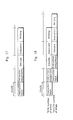
- Fig.17 is a timing diagram showing the pipeline behavior of the processor 1. As illustrated in the diagram, the pipeline of the processor 1 basically consists of the following five stages: instruction fetch; instruction assignment (dispatch); decode; execution; and writing.
- Fig.18 is a timing diagram showing each stage of the pipeline behavior of the processor 1 at the time of executing an instruction.
- the instruction fetch stage an access is made to an instruction memory which is indicated by an address specified by the program counter (PC) 33, and the instruction is transferred to the instruction buffers 10c ⁇ 10e and the like.
- the instruction assignment stage the output of branch target address information in response to a branch instruction, the output of an input register control signal, the assignment of a variable length instruction are carried out, which is followed by the transfer of the instruction to an instruction register (IR).
- the IR is inputted to the decoding unit 20, and an operation unit control signal and a memory access signal are outputted.
- an operation is executed and the result of the operation is outputted either to the data memory or the general-purpose registers (R0 ⁇ R31) 30a.
- the writing stage a value obtained as a result of data transfer, and the operation results are stored in the general-purpose registers.
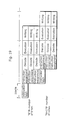
- the VLIW architecture of the processor 1 allows parallel execution of the above processing on maximum of three data elements. Therefore, the processor 1 performs the behavior shown in Fig.18 in parallel at the timing shown in Fig.19.
- Tables 3 ⁇ 5 list categorized instructions to be executed by the processor 1.
- Category Opera tion unit Instruction operation code Memory transfer instruction (load) M ld,ldh,ldhu,ldb,ldbu,ldp,ldhp,ldbp,ldbh, ldbuh,ldbhp,ldbuhp Memory transfer instruction (store) M st,sth,stb,stp,sthp,stbp,stbh,stbhp st,sth,stb,stp,sthp,stbp,stbh,stbhp Memory transfer instruction (others) M dpref,ldstb External register transfer instruction M rd,rde,wt,wte Branch instruction Branch B br,brl,call,jmp,jmpl,jmpr,ret,jmpf,jloo p,setbb,setlr,settar Software interrupt instruction interrupt B
- Fig.20 is a diagram showing the format of the instructions executed by the processor 1.
- predicate execution condition: one of the eight condition flags C0 ⁇ C7 is specified
- OP operation code field
- R register field
- I immediate field
- D displacement field.
- predicates which are flags for controlling whether or not an instruction is executed based on values of the condition flags C0 ⁇ C7, serve as a technique that allows instructions to be selectively executed without using a branch instruction and therefore that accelerates the speed of processing.
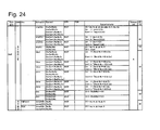
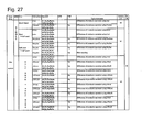
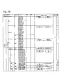
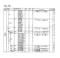
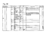
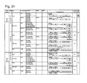
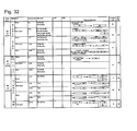
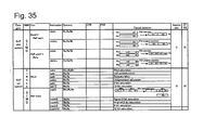
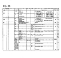
- Figs.21 ⁇ 36 are diagrams explaining outlined functionality of the instructions executed by the processor 1. More specifically, Fig.21 explains an instruction belonging to the category "ALUadd (addition) system)”; Fig.22 explains an instruction belonging to the category “ALUsub (subtraction) system)”; Fig.23 explains an instruction belonging to the category “ALUlogic (logical operation) system and others”; Fig.24 explains an instruction belonging to the category “CMP (comparison operation) system”; Fig.25 explains an instruction belonging to the category “mul (multiplication) system”; Fig.26 explains an instruction belonging to the category “mac (sum of products operation) system”; Fig.27 explains an instruction belonging to the category “msu (difference of products) system”; Fig.28 explains an instruction belonging to the category “MEMId (load from memory) system”; Fig.29 explains an instruction belonging to the category “MEMstore (store in memory) system”; Fig.30 explains an instruction belonging to the category "
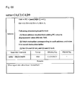
- SIMD indicates the type of an instruction (distinction between SISD (SINGLE) and SIMD); "Size” indicates the size of individual operand to be an operation target; "Instruction” indicates the operation code of an operation; “Operand” indicates the operands of an instruction; “CFR” indicates a change in the condition flag register; “PSR” indicates a change in the processor status register; "Typical behavior” indicates the overview of a behavior; “Operation unit” indicates a operation unit to be used; and “3116” indicates the size of an instruction.
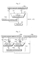
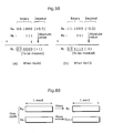
- Instruction vcchk is a SIMD instruction for judging whether results of a SIMD compare instruction (e.g. vcmpCCb) are all zero or not, and setting the results to the condition flag register (CFR) 32.
- the processor judges, as illustrated in Fig.37, whether the vector condition flags VC0 ⁇ VC3 (110) in the condition flag register (CFR) 32 are all zero or not, and sets the condition flags C4 and C5 in the condition flag resister (CFR) 32 to 1 and 0 respectively when all of the vector condition flags VC0 ⁇ VC3 (110) are zero, while setting the condition flags C4 and C5 in the condition flag resister (CFR) 32 to 0 and 1 respectively when not all the vector condition flags VC0 ⁇ VC3 (110) are zero. Then, the vector condition flags VC0 ⁇ VC3 are stored in the condition flags C0 ⁇ C3. A detailed behavior is as shown in Fig.38.
- This instruction allows a faster extraction of results of SIMD compare instructions (especially, agreement/disagreement of results), and is effective when detecting the EOF (End Of File) of a file and other purposes.
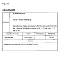
- Instruction stbh is an instruction for storing, into a memory and the like, two pieces of byte data stored in one register (byte data stored in the higher 16 bits and byte data stored in the lower 16 bits). This instruction is paired with Instruction ldbh (for moving data in the opposite direction). For example, when stbh (Ra), Rb the processor 1, using the I/F unit 50 and others, stores two pieces of byte data stored in the register Rb (the 16 ⁇ 23th bits and the 0 ⁇ 7th bits in the register Rb) into storage locations indicated by addresses specified by the register Ra, as illustrated in Fig.39. A detailed behavior is as shown in Fig.40.
- Instruction stbhp is an instruction for storing, into a memory and the like, four pieces of byte data stored in two registers (pair registers) (two pieces of byte data stored in the higher 16 bits of the respective registers and two pieces of byte data stored in the lower 16 bits of the respective registers).
- This instruction is paired with Instruction ldbhp (for moving data in the opposite direction).
- Ra the processor 1
- a detailed behavior is as shown in Fig.42.
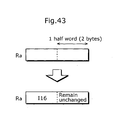
- Instruction sethi is an instruction for storing an immediate value in the higher 16 bits of a register without changing the lower 16 bits of the register.
- the processor 1 stores a 16-bit immediate value (I16) in the higher 16 bits of the register Ra, as shown in Fig.43. When this is done, there is no change in the lower 16 bits of the register Ra.
- a detailed behavior is as shown in Fig.44.
- This instruction when combined with Instruction "mov Rb, 116", makes it possible for a 32-bit immediate value to be set in a register.
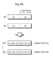
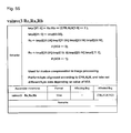
- Instruction vaddhvc is a SIMD instruction for making a switch of objects to be added, depending on the value of a vector condition flag. For example, when vaddhvc Rc, Ra, Rb the processor 1, using the operation unit 40 and others, adds the value held in the register Ra with the value held in the register Ra or Rb in the half word vector format, and stores the result into the register Rc, as shown in Fig.45. When this is done, whether the value held in Ra or the value held in Rb is added depends on a value of the vector condition flag VC2.
- This instruction is effective when used for motion compensation in image processing. Since a value resulted from dividing the value held in the addition result register Rc by 2 serves as the average value of Ra or the average value of Ra and Rb, there is an advantage that a single program can support half-pel motion compensation (motion compensation performed on a per-half-pixel basis) regardless of whether pixels are integer pixels or half pixels, as shown in Fig.47.
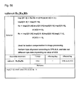
- Instruction vaddrhvc is equivalent to an instruction in which rounding is performed in addition to processing of the above-explained Instruction vaddhvc.
- the processor 1 using the arithmetic and logic/comparison operation unit 41 and others, adds the value held in the register Ra with the value held in the register Ra or Rb in the half word vector format and further adds 1 for rounding, and stores the result into the register Rc, as shown in Fig.48.
- Other behavior is equivalent to that of Instruction vaddhvc. A detailed behavior is as shown in Fig.49.
- This instruction is also effective when used for motion compensation in image processing.
- vaddhvc and vaddrhvc 1-bit shift right (processing to perform a division by 2) may be added. Such functionality enables a processor to directly determine pixel values of integer pixels and half pixels.
- an instruction having functionalities of both Instruction vaddhvc and Instruction vaddrhvc may be also possible to define an instruction having functionalities of both Instruction vaddhvc and Instruction vaddrhvc.
- An example of such instruction is one which is capable of behaving either as Instruction v addhvc or Instruction vaddhrvc depending on a value of a condition flag. Such instruction allows a single program to perform processing regardless of whether rounding is performed or not.
- Instruction vsgnh is a SIMD instruction for generating a value depending on the sign (positive/negative) of the value held in a register and whether a value held in a register is zero or not.
- the processor 1 stores one of the following values into the register Rb in half word vector format, as shown in Fig.50:( ( i ) 1 when the . value held in the register Ra is positive, ( ii ) -1 when the value held in the register Ra is negative, and ( iii ) 0 when the value held in the register Ra is 0.
- a detailed behavior is as shown in Fig.51.
- This instruction is effective when used for inverse quantization in image processing since 1 is outputted when a certain value is positive, -1 when negative, and 0 when 0.
- values on which SIMD operations are difficult to be performed can be calculated at an increased speed.
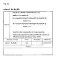
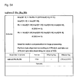
- Instruction valnvc1 is a SIMD instruction for byte-aligning data and e xtracting different b yte d ata d epending on a vector condition flag.
- the processor 1 performs byte-alignment by shifting a bit string resulted from concatenating the registers Ra and Rb according to a value indicated by Bit ALN[1:0] of the condition flag register (CFR) 32, and stores four pieces of byte data which have been extracted depending on a value of the vector condition flag VC0, as shown in Fig.52.
- a detailed behavior is as shown in Fig.53.
- This instruction is effective when used for motion compensation in image processing. Since a value resulted from dividing the value held in the addition result register Rc by 2 on a per-half word vector basis equals to "a" and "b", or (a+b)/2 and (b+c)/2, there is an advantage that a single program can support half-pel motion compensation (motion compensation performed on a per-half-pixel basis) regardless of whether pixels are integer pixels or half pixels, as shown in Fig.47.
- the present invention is not limited to byte as a unit of alignment, and therefore that half word and half byte may also serve as a unit of alignment.
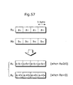
- Instruction addarvw is an instruction for adding two values and further adding 1 when one of such values is positive.
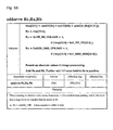
- the processor 1 uses the arithmetic and logic/comparison operation unit 41 and others, adds the value held in the register Ra and the value held in the register Rb, as shown in Fig.57. When this is done, the processor 1 further adds 1 when the value held in the register Ra is positive.
- a detailed behavior is as shown in Fig.58.
- This instruction is effective when used for "rounding of an absolute value (away from zero)".
- a value to be rounded is stored in the register Ra, and a value resulted from filling, with 1, a bit corresponding to one lower than the bit to be rounded shall be stored in the register Rb.
- a result generated by rounding the absolute value of the value held in the register Ra here, the most significant bit is a sign bit, and therefore the value held in Ra is fixed point data which has a point between the second bit and the third bit from the most significant bit
- the register Rc is to be stored in the register Rc.
- Instruction movp is an instruction for moving values held in arbitrary two registers to two consecutive registers. For example, when movp Rc: Rc+1, Ra, Rb the processor 1, using the I/F unit 50 and others, moves the value held in the register Ra to the register Rc, and moves the value held in the register Rb to the register Rc+1, as shown in Fig.60. A detailed behavior is as shown in Fig.61.
- this instruction Since values held in independent two registers are moved in one cycle under this instruction, an effect of reducing the number of cycles in a loop can be achieved. Also, this instruction, which does not involve register renaming (destruction of a register value), is effective when data is moved between loop generations (iterations).
- move is not an exclusive type of operations, and therefore unary operations (e.g. "neg") and binary operations ("add”) are also in the scope of the present invention.
- add binary operations
- Instruction jloop is an instruction for performing branches and setting condition flags (predicates, here) in a loop.
- the processor 1 behaves as follows, using the address management unit 10b and others: ( i ) sets 1 to the condition flag Cm; ( ii ) sets 0 to the condition flag C6 when the value held in the register Ra is . smaller than 0; ( iii ) adds -1 to the value held in the register Ra and stores the result into the register Ra; and ( iv ) branches to an address specified by the branch register (TAR) 30d.
- the jump buffer 10f branch instruction buffer
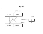
- a detailed behavior is as shown in Fig.62.
- Instruction settar is an instruction for storing a branch target address in the branch register (TAR) 30d, and setting condition flags (predicates, here).
- the processor 1 behaves as follows, using the address management unit 10b and others: ( i ) stores an address resulted from adding the value held in the program counter (PC) 33 and a displacement value (D9) into the branch register (TAR) 30d; ( ii ) fetches the instruction corresponding to such address and stores it in the jump buffer 10f (branch instruction buffer); and ( iii ) sets the condition flag C6 to 1 and the condition flag Cm to 0.
- a detailed behavior is as shown in Fig.63.
- PROLOG/EPILOG removal is intended to visually remove a PROLOG portion and an EPILOG portion by using the PROLOG portion and the EPILOG portion as condition execution instructions to be performed according to predicates, as shown in Fig.64.
- condition flags C6 and C4 are illustrated as predicates for an EPILOG instruction (Stage 2) and a PROLOG instruction (Stage 1), respectively.
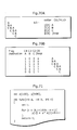
- a compiler when the ordinary jloop and settar instructions are used in a source program written in the C language shown in Fig.65, a compiler generates a machine language program shown in Fig.66 by means of PROLOG/EPILOG removal software pipelining. As indicated by the loop part in such machine language program (Label L00023 ⁇ Instruction jloop), 3 cycles are involved in loop execution since an instruction for setting the condition flag C4 (Instruction cmpeq) is required. Furthermore, two instructions are required for the setting and resetting of the condition flag C4, reducing the effect of PROLOG/EPILOG removal.
- Instruction “jloop C6, Cm, TAR, Ra” and Instruction “settar C6, Cm, D9” are effective for reducing the number of execution cycles in 2-stage PROLOG/EPILOG removal software pipelining.
- processor 1 supports instructions which are applicable not only to 2-stage software pipelining, but also to 3-stage software pipelining: Instruction “jloop C6, C2: C4, TAR, Ra” and Instruction “settar C6, C2: C4, D9". These instructions “jloop C6, C2: C4, TAR, Ra” and “settar C6, C2: C4, D9” are equivalent to instructions in which the register Cm in the above-described 2-stage instructions “jloop C6, Cm, TAR, Ra” and “settar C6, Cm, D9" are extended to the registers C2, C3 and C4.
- the processor 1 behaves as follows, using the address management unit 10b and others: ( i ) sets the condition flag C4 to 0 when the value held in the register Ra is smaller than 0; ( ii ) moves the value of the condition flag C3 to the condition flag C2 and moves the value of the condition flag C4 to the condition flags C3 and C6; ( iii ) adds - 1 to the register Ra and stores the result into the register Ra; and ( iv ) branches to an address specified by the branch register (TAR) 30d.
- the jump buffer 10f (branch instruction buffer) is filled with a branch target instruction.
- a detailed behavior is as shown in Fig.68.
- the processor 1 behaves as follows, using the address management unit 10b and others: ( i ) stores an address resulted from adding the value held in the program counter (PC) 33 and a displacement value (D9) into the branch register (TAR) 30d; ( ii ) fetches the instruction corresponding to such address and stores it in the jump buffer 10f (branch instruction buffer); and ( iii ) sets the condition flags C4 and C6 to 1 and the condition flags C2 and C3 to 0. A detailed behavior is as shown in Fig.69.
- Figs.70A and 70B show the role of the condition flags in the above 3-stage instructions “jloop C6, C2: C4, TAR, Ra" and "settar C6, C2: C4, D9".
- the condition flags C2, C3 and C4 are predicates intended for Stage 3, Stage 2 and Stage 1, respectively.
- Fig.70B is a diagram showing how instruction execution is going on when moving flags in such a case.
- Figs.71 ⁇ 73 show program examples illustrating the significance of moving flags in the above instructions "jloop C6, C2: C4, TAR, Ra" and "settar C6, C2: C4, D9".
- Fig.71 shows an example of a source program
- Fig.72 shows an example of a machine language program created by using ordinary instructions jloop and settar without the functionality of moving flags
- Fig.73 shows an example of a machine language program created by using Instruction jloop and Instruction settar according to the present embodiment that have the functionality of moving flags.
- the processor 1 is also capable of executing the following characteristic instructions which are not shown in Figs.21 ⁇ 36.
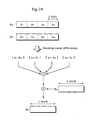
- Instruction vsada is a SIMD instruction for determining a sum of absolute value differences.
- the processor 1 using the arithmetic and logic/comparison operation unit 41 and others, performs SIMD operations for determining differences between the values held in the register Ra and the values held in the register Rb on a byte-by-byte basis (determines the difference between the respective four byte pairs), as shown in Fig.74, determines the absolute value of each of the four results so as to add them, adds the value held in the register Rx to this addition result, and stores the final result into the register Rc.
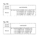
- a detailed behavior is as shown in Fig.75A.
- the processor 1 is also capable of executing an instruction which does not include the last operand (Rx) in the format of the above Instruction vsada.
- the processor 1 using the arithmetic and logic/comparison operation unit 41 and others, performs SIMD operations for determining differences between the values held in the register Ra and the values held in the register Rb on a byte-by-byte basis (determines the difference between the respective four byte pairs), determines the absolute value of each of the four results so as to add them, and stores the result into the register Rc.
- SIMD operations for determining differences between the values held in the register Ra and the values held in the register Rb on a byte-by-byte basis (determines the difference between the respective four byte pairs), determines the absolute value of each of the four results so as to add them, and stores the result into the register Rc.
- Fig.75B A detailed behavior is as shown in Fig.75B.
- Instruction vasubb is a SIMD instruction for performing subtractions on four pairs of SIMD data on a byte-by-byte basis, and storing the resulting four signs in the condition flag register.
- Instruction vabssumb is a SIMD instruction for adding the absolute values of four pairs of SIMD data on a byte-by-byte basis according to the condition flag register, and adding this addition result to another 4-byte data.
- Instruction vsada makes it possible for a sum of absolute value differences to be determined in one cycle and therefore makes faster the speed of operations, as compared with the case where Instruction vasubb and Instruction vabssumb are used in succession.
- Instruction vasada is effective when used for summing up absolute value differences in motion prediction as part of image processing.
- Instruction satss is an instruction for converting a signed value into a saturated signed value at an arbitrary position (digit). For example, when satss Rc, Ra, Rb the processor 1, using the saturation block (SAT) 47a and others, stores, into the register Rc, a saturated value (complement on 1 of the register Rb) specified by the register Rb when the value held in the register Ra is larger than such saturated value, and stores the value held in the register Ra into the register Rc when the value held in the register Ra is equal to or smaller than the saturated value, as illustrated in Fig.76. A detailed behavior is as shown in Fig.77A.
- Instruction satsu is an instruction for converting an unsigned value into a saturated signed value at an arbitrary position (digit).
- the processor 1 using the saturation block (SAT) 47a and others, stores a saturated value specified by the register Rb into the register Rc when the value held in the register Ra is larger than such saturated value, and stores the value held in the register Ra into the register Rc when the value held in the register Ra is equal to or smaller than the saturated value.
- SAT saturation block
- Instruction satss and Instruction satsu allow saturation processing to be performed at an arbitrary position. This facilitates programming since there is no need for setting a position where saturation is performed to a specific position at the time of assembler programming.
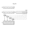
- Instruction bytesel is an instruction for selecting one of the values held in two registers on a byte-by-byte basis.
- the processor 1 using the operation unit 40 and others, stores one of eight pieces of byte data held in the register Ra and the register Rb into the register Rc, on the basis of a value indicated by the register Rx, as illustrated in Fig.78.
- This behavior is performed on four pieces of bytes in the register Rc in parallel.
- a detailed behavior is shown in Fig.79A, and a relationship between the register Rx and byte data to be selected is shown in Fig.79B.
- the processor 1 behaves in an equivalent manner also for Instruction bytesel in the following format: when bytesel Rc, Ra, Rb, 112 the processor 1, using the operation unit 40 and others, stores one of eight pieces of byte data held in the register Ra and the register Rb into the register Rc, on the basis of a 12-bit immediate value. This behavior is performed on four pieces of bytes in the register Rc in parallel. A detailed behavior is shown in Fig.79C, and a relationship between an immediate value 112 and byte data to be selected is shown in Fig.79D.
- Instruction bytesel allows byte data to be stored at an arbitrary position in a register, and therefore makes repetitions of data reshuffling faster. Moreover, this instruction has an effect of increasing the flexibility of SIMD operations.
- the processor 1 is also capable of executing SIMD operation-related complementary processing, in addition to the above-explained instructions.
- the processor1 when a certain instruction is issued, performs complementary processing for extending a part of results of SIMD operations (sign extension or zero extension), as illustrated in Figs.80A and 80B, which show the processor 1 performing SIMD operations on data at the same positions in respective registers (to be referred to also as "straight positions" hereinafter) or on data at diagonally crossed positions, on a per-half word basis.
- Fig.80A illustrates processing for extending the lower half word of a required result to a word
- Fig.80B illustrates processing for extending the higher half word of a required result to a word.
- Instruction vaddh is an example instruction for performing SIMD operations on data at straight positions on a per-half word basis
- Instruction vxaddh is an example instruction for performing SIMD operations on data at diagonally crossed positions on a per-half word basis.
- Fig.81 illustrates the processor 1 performing SIMD operations on pieces of data stored at straight positions or diagonally crossed positions in two registers on a per-half word basis, as well as extending each of resulting two half words to a word.
- Such an instruction for extending results of SIMD operation as above is effective when making data size all the same by performing sign extension or zero extension after performing the SIMD operations, enabling SIMD operations and extension processing to be performed in one cycle.
- the processor 1 is also capable of executing SIMD operations specified by condition flags and the like, as SIMD operation-related complementary instructions.
- condition flags specify that the first and the second operations should be "addition” and “subtraction” respectively, performs additions and subtractions on each of data pairs in two registers at straight positions or diagonally crossed positions on a per-half word basis, as illustrated in Fig.82.
- the processor 1 behaves as follows, using the arithmetic and logic/comparison operation unit 41 and others:
- Such an instruction in which types of SIMD operations are specifiable is effective for processing in which types of operations to be performed are not fixed, and therefore in which an operation shall be determined depending on a result of other processing.
- the processor 1 may:
Landscapes
- Engineering & Computer Science (AREA)
- Software Systems (AREA)
- Theoretical Computer Science (AREA)
- Physics & Mathematics (AREA)
- General Physics & Mathematics (AREA)
- General Engineering & Computer Science (AREA)
- Mathematical Physics (AREA)
- Computational Mathematics (AREA)
- Mathematical Analysis (AREA)
- Mathematical Optimization (AREA)
- Pure & Applied Mathematics (AREA)
- Executing Machine-Instructions (AREA)
- Advance Control (AREA)
Applications Claiming Priority (2)
| Application Number | Priority Date | Filing Date | Title |
|---|---|---|---|
| JP2002280077A JP3958662B2 (ja) | 2002-09-25 | 2002-09-25 | プロセッサ |
| JP2002280077 | 2002-09-25 |
Publications (2)
| Publication Number | Publication Date |
|---|---|
| EP1403762A2 true EP1403762A2 (de) | 2004-03-31 |
| EP1403762A3 EP1403762A3 (de) | 2007-12-12 |
Family
ID=31973293
Family Applications (1)
| Application Number | Title | Priority Date | Filing Date |
|---|---|---|---|
| EP03020559A Withdrawn EP1403762A3 (de) | 2002-09-25 | 2003-09-17 | SIMD Befehle ausführender Prozessor |
Country Status (6)
| Country | Link |
|---|---|
| US (5) | US7281117B2 (de) |
| EP (1) | EP1403762A3 (de) |
| JP (1) | JP3958662B2 (de) |
| KR (1) | KR20040027409A (de) |
| CN (1) | CN100524204C (de) |
| TW (2) | TW200411542A (de) |
Cited By (2)
| Publication number | Priority date | Publication date | Assignee | Title |
|---|---|---|---|---|
| CN103970508A (zh) * | 2014-06-04 | 2014-08-06 | 上海航天电子通讯设备研究所 | 一种精简的微处理器ip核 |
| RU2531862C2 (ru) * | 2009-12-25 | 2014-10-27 | Интел Корпорейшн | Быстрое векторное вычисление деления без ветвления |
Families Citing this family (95)
| Publication number | Priority date | Publication date | Assignee | Title |
|---|---|---|---|---|
| US7392368B2 (en) * | 2002-08-09 | 2008-06-24 | Marvell International Ltd. | Cross multiply and add instruction and multiply and subtract instruction SIMD execution on real and imaginary components of a plurality of complex data elements |
| US7861007B2 (en) * | 2003-12-05 | 2010-12-28 | Ati Technologies Ulc | Method and apparatus for multimedia display in a mobile device |
| US7676476B2 (en) * | 2004-08-25 | 2010-03-09 | Microsoft Corporation | Data types with incorporated collation information |
| US7219213B2 (en) * | 2004-12-17 | 2007-05-15 | Intel Corporation | Flag bits evaluation for multiple vector SIMD channels execution |
| US7512826B2 (en) * | 2005-04-20 | 2009-03-31 | International Business Machines Corporation | Method, apparatus, and product for an efficient virtualized time base in a scaleable multi-processor computer |
| US20070186210A1 (en) * | 2006-02-06 | 2007-08-09 | Via Technologies, Inc. | Instruction set encoding in a dual-mode computer processing environment |
| US7676647B2 (en) * | 2006-08-18 | 2010-03-09 | Qualcomm Incorporated | System and method of processing data using scalar/vector instructions |
| US9069547B2 (en) * | 2006-09-22 | 2015-06-30 | Intel Corporation | Instruction and logic for processing text strings |
| US7752028B2 (en) | 2007-07-26 | 2010-07-06 | Microsoft Corporation | Signed/unsigned integer guest compare instructions using unsigned host compare instructions for precise architecture emulation |
| JP5092722B2 (ja) | 2007-12-07 | 2012-12-05 | ソニー株式会社 | 画像処理装置、画像処理方法およびプログラム |
| US8041927B2 (en) * | 2008-04-16 | 2011-10-18 | Nec Corporation | Processor apparatus and method of processing multiple data by single instructions |
| US7996647B2 (en) * | 2008-07-23 | 2011-08-09 | Microchip Technology Incorporated | Enhanced microprocessor or microcontroller |
| US8271832B2 (en) * | 2008-08-15 | 2012-09-18 | Apple Inc. | Non-faulting and first-faulting instructions for processing vectors |
| US8938642B2 (en) * | 2008-08-15 | 2015-01-20 | Apple Inc. | Confirm instruction for processing vectors |
| US8862932B2 (en) * | 2008-08-15 | 2014-10-14 | Apple Inc. | Read XF instruction for processing vectors |
| US9009528B2 (en) * | 2008-08-15 | 2015-04-14 | Apple Inc. | Scalar readXF instruction for processing vectors |
| JP5438551B2 (ja) | 2009-04-23 | 2014-03-12 | 新日鉄住金ソリューションズ株式会社 | 情報処理装置、情報処理方法及びプログラム |
| GB2474901B (en) * | 2009-10-30 | 2015-01-07 | Advanced Risc Mach Ltd | Apparatus and method for performing multiply-accumulate operations |
| GB2480285A (en) | 2010-05-11 | 2011-11-16 | Advanced Risc Mach Ltd | Conditional compare instruction which sets a condition code when it is not executed |
| CN102270112A (zh) * | 2010-06-03 | 2011-12-07 | 边立剑 | Risc微处理器指令译码电路 |
| US20120084539A1 (en) * | 2010-09-29 | 2012-04-05 | Nyland Lars S | Method and sytem for predicate-controlled multi-function instructions |
| JP5659772B2 (ja) * | 2010-12-17 | 2015-01-28 | 富士通株式会社 | 演算処理装置 |
| US8880857B2 (en) | 2011-04-07 | 2014-11-04 | Via Technologies, Inc. | Conditional ALU instruction pre-shift-generated carry flag propagation between microinstructions in read-port limited register file microprocessor |
| US8880851B2 (en) | 2011-04-07 | 2014-11-04 | Via Technologies, Inc. | Microprocessor that performs X86 ISA and arm ISA machine language program instructions by hardware translation into microinstructions executed by common execution pipeline |
| US9176733B2 (en) | 2011-04-07 | 2015-11-03 | Via Technologies, Inc. | Load multiple and store multiple instructions in a microprocessor that emulates banked registers |
| US9898291B2 (en) | 2011-04-07 | 2018-02-20 | Via Technologies, Inc. | Microprocessor with arm and X86 instruction length decoders |
| US9032189B2 (en) * | 2011-04-07 | 2015-05-12 | Via Technologies, Inc. | Efficient conditional ALU instruction in read-port limited register file microprocessor |
| US9244686B2 (en) | 2011-04-07 | 2016-01-26 | Via Technologies, Inc. | Microprocessor that translates conditional load/store instructions into variable number of microinstructions |
| US9141389B2 (en) | 2011-04-07 | 2015-09-22 | Via Technologies, Inc. | Heterogeneous ISA microprocessor with shared hardware ISA registers |
| US9336180B2 (en) | 2011-04-07 | 2016-05-10 | Via Technologies, Inc. | Microprocessor that makes 64-bit general purpose registers available in MSR address space while operating in non-64-bit mode |
| US9043580B2 (en) | 2011-04-07 | 2015-05-26 | Via Technologies, Inc. | Accessing model specific registers (MSR) with different sets of distinct microinstructions for instructions of different instruction set architecture (ISA) |
| US9645822B2 (en) | 2011-04-07 | 2017-05-09 | Via Technologies, Inc | Conditional store instructions in an out-of-order execution microprocessor |
| US8924695B2 (en) | 2011-04-07 | 2014-12-30 | Via Technologies, Inc. | Conditional ALU instruction condition satisfaction propagation between microinstructions in read-port limited register file microprocessor |
| US9128701B2 (en) | 2011-04-07 | 2015-09-08 | Via Technologies, Inc. | Generating constant for microinstructions from modified immediate field during instruction translation |
| US9317288B2 (en) | 2011-04-07 | 2016-04-19 | Via Technologies, Inc. | Multi-core microprocessor that performs x86 ISA and ARM ISA machine language program instructions by hardware translation into microinstructions executed by common execution pipeline |
| US9292470B2 (en) | 2011-04-07 | 2016-03-22 | Via Technologies, Inc. | Microprocessor that enables ARM ISA program to access 64-bit general purpose registers written by x86 ISA program |
| US9378019B2 (en) | 2011-04-07 | 2016-06-28 | Via Technologies, Inc. | Conditional load instructions in an out-of-order execution microprocessor |
| US9146742B2 (en) | 2011-04-07 | 2015-09-29 | Via Technologies, Inc. | Heterogeneous ISA microprocessor that preserves non-ISA-specific configuration state when reset to different ISA |
| US9274795B2 (en) | 2011-04-07 | 2016-03-01 | Via Technologies, Inc. | Conditional non-branch instruction prediction |
| US8949777B2 (en) * | 2011-04-22 | 2015-02-03 | Intel Corporation | Methods and systems for mapping a function pointer to the device code |
| CN102411490B (zh) * | 2011-08-09 | 2014-04-16 | 清华大学 | 一种针对动态可重构处理器的指令集的优化方法 |
| US10534606B2 (en) | 2011-12-08 | 2020-01-14 | Oracle International Corporation | Run-length encoding decompression |
| CN104025033B (zh) * | 2011-12-30 | 2017-11-21 | 英特尔公司 | 利用控制操纵的simd可变移位和循环 |
| US9575753B2 (en) * | 2012-03-15 | 2017-02-21 | International Business Machines Corporation | SIMD compare instruction using permute logic for distributed register files |
| US8898433B2 (en) * | 2012-04-26 | 2014-11-25 | Avago Technologies General Ip (Singapore) Pte. Ltd. | Efficient extraction of execution sets from fetch sets |
| US9038042B2 (en) | 2012-06-29 | 2015-05-19 | Analog Devices, Inc. | Staged loop instructions |
| US9378017B2 (en) * | 2012-12-29 | 2016-06-28 | Intel Corporation | Apparatus and method of efficient vector roll operation |
| US20140244987A1 (en) * | 2013-02-22 | 2014-08-28 | Mips Technologies, Inc. | Precision Exception Signaling for Multiple Data Architecture |
| JP2015049832A (ja) | 2013-09-04 | 2015-03-16 | インターナショナル・ビジネス・マシーンズ・コーポレーションInternational Business Machines Corporation | 定数ロードのオーバーヘッドを削減する方法、装置及びプログラム |
| US11113054B2 (en) | 2013-09-10 | 2021-09-07 | Oracle International Corporation | Efficient hardware instructions for single instruction multiple data processors: fast fixed-length value compression |
| US9430390B2 (en) * | 2013-09-21 | 2016-08-30 | Oracle International Corporation | Core in-memory space and object management architecture in a traditional RDBMS supporting DW and OLTP applications |
| US9697005B2 (en) * | 2013-12-04 | 2017-07-04 | Analog Devices, Inc. | Thread offset counter |
| JP2015143949A (ja) * | 2014-01-31 | 2015-08-06 | 富士通株式会社 | 演算プログラム、演算装置および演算方法 |
| CN104317554B (zh) * | 2014-10-14 | 2017-02-15 | 中国航天科技集团公司第九研究院第七七一研究所 | 用于simd处理器的寄存器文件数据读写装置和方法 |
| US20160179538A1 (en) * | 2014-12-19 | 2016-06-23 | Intel Corporation | Method and apparatus for implementing and maintaining a stack of predicate values with stack synchronization instructions in an out of order hardware software co-designed processor |
| US9817791B2 (en) | 2015-04-04 | 2017-11-14 | Texas Instruments Incorporated | Low energy accelerator processor architecture with short parallel instruction word |
| US11847427B2 (en) * | 2015-04-04 | 2023-12-19 | Texas Instruments Incorporated | Load store circuit with dedicated single or dual bit shift circuit and opcodes for low power accelerator processor |
| US9952865B2 (en) | 2015-04-04 | 2018-04-24 | Texas Instruments Incorporated | Low energy accelerator processor architecture with short parallel instruction word and non-orthogonal register data file |
| US10025823B2 (en) | 2015-05-29 | 2018-07-17 | Oracle International Corporation | Techniques for evaluating query predicates during in-memory table scans |
| US10620952B2 (en) | 2015-06-24 | 2020-04-14 | International Business Machines Corporation | Conversion of boolean conditions |
| US10698688B2 (en) * | 2015-06-24 | 2020-06-30 | International Business Machines Corporation | Efficient quantization of compare results |
| US10705841B2 (en) | 2015-06-24 | 2020-07-07 | International Business Machines Corporation | Instruction to perform a logical operation on conditions and to quantize the Boolean result of that operation |
| US10067954B2 (en) | 2015-07-22 | 2018-09-04 | Oracle International Corporation | Use of dynamic dictionary encoding with an associated hash table to support many-to-many joins and aggregations |
| GB2540939B (en) * | 2015-07-31 | 2019-01-23 | Advanced Risc Mach Ltd | An apparatus and method for performing a splice operation |
| GB2540941B (en) * | 2015-07-31 | 2017-11-15 | Advanced Risc Mach Ltd | Data processing |
| US20170177369A1 (en) * | 2015-12-21 | 2017-06-22 | Intel Corporation | Non-contiguous multiple register access for microprocessor data exchange instructions |
| US10503474B2 (en) | 2015-12-31 | 2019-12-10 | Texas Instruments Incorporated | Methods and instructions for 32-bit arithmetic support using 16-bit multiply and 32-bit addition |
| US10061832B2 (en) | 2016-11-28 | 2018-08-28 | Oracle International Corporation | Database tuple-encoding-aware data partitioning in a direct memory access engine |
| US10055358B2 (en) | 2016-03-18 | 2018-08-21 | Oracle International Corporation | Run length encoding aware direct memory access filtering engine for scratchpad enabled multicore processors |
| US10061714B2 (en) | 2016-03-18 | 2018-08-28 | Oracle International Corporation | Tuple encoding aware direct memory access engine for scratchpad enabled multicore processors |
| US10402425B2 (en) | 2016-03-18 | 2019-09-03 | Oracle International Corporation | Tuple encoding aware direct memory access engine for scratchpad enabled multi-core processors |
| US10599488B2 (en) | 2016-06-29 | 2020-03-24 | Oracle International Corporation | Multi-purpose events for notification and sequence control in multi-core processor systems |
| US10380058B2 (en) | 2016-09-06 | 2019-08-13 | Oracle International Corporation | Processor core to coprocessor interface with FIFO semantics |
| US10783102B2 (en) | 2016-10-11 | 2020-09-22 | Oracle International Corporation | Dynamically configurable high performance database-aware hash engine |
| US10176114B2 (en) | 2016-11-28 | 2019-01-08 | Oracle International Corporation | Row identification number generation in database direct memory access engine |
| US10459859B2 (en) | 2016-11-28 | 2019-10-29 | Oracle International Corporation | Multicast copy ring for database direct memory access filtering engine |
| US10725947B2 (en) | 2016-11-29 | 2020-07-28 | Oracle International Corporation | Bit vector gather row count calculation and handling in direct memory access engine |
| EP3336692B1 (de) * | 2016-12-13 | 2020-04-29 | Arm Ltd | Replikatpartitionsanweisung |
| EP3336691B1 (de) | 2016-12-13 | 2022-04-06 | ARM Limited | Replikatelementanweisung |
| US10401412B2 (en) | 2016-12-16 | 2019-09-03 | Texas Instruments Incorporated | Line fault signature analysis |
| US20190102182A1 (en) * | 2017-09-29 | 2019-04-04 | Intel Corporation | Apparatus and method for performing dual signed and unsigned multiplication of packed data elements |
| US10514924B2 (en) | 2017-09-29 | 2019-12-24 | Intel Corporation | Apparatus and method for performing dual signed and unsigned multiplication of packed data elements |
| US10795676B2 (en) | 2017-09-29 | 2020-10-06 | Intel Corporation | Apparatus and method for multiplication and accumulation of complex and real packed data elements |
| US10534838B2 (en) | 2017-09-29 | 2020-01-14 | Intel Corporation | Bit matrix multiplication |
| US10664277B2 (en) | 2017-09-29 | 2020-05-26 | Intel Corporation | Systems, apparatuses and methods for dual complex by complex conjugate multiply of signed words |
| US10552154B2 (en) | 2017-09-29 | 2020-02-04 | Intel Corporation | Apparatus and method for multiplication and accumulation of complex and real packed data elements |
| US10802826B2 (en) | 2017-09-29 | 2020-10-13 | Intel Corporation | Apparatus and method for performing dual signed and unsigned multiplication of packed data elements |
| US11243765B2 (en) | 2017-09-29 | 2022-02-08 | Intel Corporation | Apparatus and method for scaling pre-scaled results of complex multiply-accumulate operations on packed real and imaginary data elements |
| US10795677B2 (en) | 2017-09-29 | 2020-10-06 | Intel Corporation | Systems, apparatuses, and methods for multiplication, negation, and accumulation of vector packed signed values |
| US11256504B2 (en) | 2017-09-29 | 2022-02-22 | Intel Corporation | Apparatus and method for complex by complex conjugate multiplication |
| US11074073B2 (en) | 2017-09-29 | 2021-07-27 | Intel Corporation | Apparatus and method for multiply, add/subtract, and accumulate of packed data elements |
| US11113061B2 (en) * | 2019-09-26 | 2021-09-07 | Advanced Micro Devices, Inc. | Register saving for function calling |
| CN111026736B (zh) * | 2019-12-13 | 2024-03-12 | 中盈优创资讯科技有限公司 | 数据血缘管理方法及装置、数据血缘解析方法及装置 |
| CN116009965A (zh) * | 2023-01-13 | 2023-04-25 | 广东省大湾区集成电路与系统应用研究院 | 一种加速risc-v指令集矢量运算方法、装置及介质 |
| CN119045894B (zh) * | 2024-07-29 | 2025-12-12 | 武汉大学 | 多标量乘法运算方法、装置、设备及存储介质 |
Family Cites Families (16)
| Publication number | Priority date | Publication date | Assignee | Title |
|---|---|---|---|---|
| JP2703884B2 (ja) | 1985-12-27 | 1998-01-26 | 日本電気株式会社 | データ書込み制御方式 |
| US5036454A (en) | 1987-05-01 | 1991-07-30 | Hewlett-Packard Company | Horizontal computer having register multiconnect for execution of a loop with overlapped code |
| US5303355A (en) | 1991-03-27 | 1994-04-12 | Motorola, Inc. | Pipelined data processor which conditionally executes a predetermined looping instruction in hardware |
| US5590352A (en) * | 1994-04-26 | 1996-12-31 | Advanced Micro Devices, Inc. | Dependency checking and forwarding of variable width operands |
| CN1153129C (zh) | 1995-09-01 | 2004-06-09 | 菲利浦电子北美公司 | 用于处理器定制操作的设备 |
| US5793658A (en) * | 1996-01-17 | 1998-08-11 | Digital Equipment Coporation | Method and apparatus for viedo compression and decompression using high speed discrete cosine transform |
| JP3701401B2 (ja) * | 1996-08-12 | 2005-09-28 | 株式会社ルネサステクノロジ | 飽和演算命令を有するマイクロプロセッサ |
| US6260137B1 (en) * | 1997-09-12 | 2001-07-10 | Siemens Aktiengesellschaft | Data processing unit with digital signal processing capabilities |
| JP2000020486A (ja) | 1998-06-29 | 2000-01-21 | Ricoh Co Ltd | Simd型演算器 |
| JP3652518B2 (ja) | 1998-07-31 | 2005-05-25 | 株式会社リコー | Simd方式の演算器及び演算処理装置 |
| JP5052713B2 (ja) | 1998-10-09 | 2012-10-17 | コーニンクレッカ フィリップス エレクトロニクス エヌ ヴィ | 条件付き命令を備えるベクトルデータプロセッサ |
| US6829696B1 (en) * | 1999-12-30 | 2004-12-07 | Texas Instruments Incorporated | Data processing system with register store/load utilizing data packing/unpacking |
| JP2001229021A (ja) * | 2000-02-18 | 2001-08-24 | Mitsubishi Electric Corp | データ処理装置 |
| US7124160B2 (en) * | 2000-03-08 | 2006-10-17 | Sun Microsystems, Inc. | Processing architecture having parallel arithmetic capability |
| US7558816B2 (en) * | 2001-11-21 | 2009-07-07 | Sun Microsystems, Inc. | Methods and apparatus for performing pixel average operations |
| US7035331B2 (en) * | 2002-02-20 | 2006-04-25 | Intel Corporation | Method and apparatus for performing a pixel averaging instruction |
-
2002
- 2002-09-25 JP JP2002280077A patent/JP3958662B2/ja not_active Expired - Lifetime
-
2003
- 2003-09-17 EP EP03020559A patent/EP1403762A3/de not_active Withdrawn
- 2003-09-24 TW TW092126392A patent/TW200411542A/zh unknown
- 2003-09-24 TW TW098124440A patent/TW200945190A/zh unknown
- 2003-09-24 US US10/668,358 patent/US7281117B2/en not_active Expired - Lifetime
- 2003-09-25 CN CNB031603653A patent/CN100524204C/zh not_active Expired - Lifetime
- 2003-09-25 KR KR1020030066510A patent/KR20040027409A/ko not_active Abandoned
-
2007
- 2007-08-31 US US11/896,368 patent/US7594099B2/en not_active Expired - Lifetime
- 2007-08-31 US US11/896,371 patent/US20080046704A1/en not_active Abandoned
- 2007-08-31 US US11/896,370 patent/US20080046690A1/en not_active Abandoned
- 2007-08-31 US US11/896,369 patent/US20080046688A1/en not_active Abandoned
Non-Patent Citations (1)
| Title |
|---|
| No Search * |
Cited By (2)
| Publication number | Priority date | Publication date | Assignee | Title |
|---|---|---|---|---|
| RU2531862C2 (ru) * | 2009-12-25 | 2014-10-27 | Интел Корпорейшн | Быстрое векторное вычисление деления без ветвления |
| CN103970508A (zh) * | 2014-06-04 | 2014-08-06 | 上海航天电子通讯设备研究所 | 一种精简的微处理器ip核 |
Also Published As
| Publication number | Publication date |
|---|---|
| US20040068642A1 (en) | 2004-04-08 |
| US7594099B2 (en) | 2009-09-22 |
| EP1403762A3 (de) | 2007-12-12 |
| US20080046690A1 (en) | 2008-02-21 |
| US20080046687A1 (en) | 2008-02-21 |
| CN1497435A (zh) | 2004-05-19 |
| KR20040027409A (ko) | 2004-04-01 |
| TW200945190A (en) | 2009-11-01 |
| TW200411542A (en) | 2004-07-01 |
| US7281117B2 (en) | 2007-10-09 |
| US20080046688A1 (en) | 2008-02-21 |
| CN100524204C (zh) | 2009-08-05 |
| JP3958662B2 (ja) | 2007-08-15 |
| JP2004118470A (ja) | 2004-04-15 |
| US20080046704A1 (en) | 2008-02-21 |
Similar Documents
| Publication | Publication Date | Title |
|---|---|---|
| US7594099B2 (en) | Processor executing SIMD instructions | |
| US7380112B2 (en) | Processor and compiler for decoding an instruction and executing the decoded instruction with conditional execution flags | |
| US7185176B2 (en) | Processor executing SIMD instructions | |
| US7284241B2 (en) | Compiler, compiler apparatus and compilation method | |
| US7430578B2 (en) | Method and apparatus for performing multiply-add operations on packed byte data | |
| JP4064989B2 (ja) | パック・データの乗加算演算を実行する装置 | |
| US7395298B2 (en) | Method and apparatus for performing multiply-add operations on packed data | |
| RU2263947C2 (ru) | Целочисленное умножение высокого порядка с округлением и сдвигом в архитектуре с одним потоком команд и множеством потоков данных | |
| US20100175056A1 (en) | Compiler apparatus with flexible optimization | |
| JP2006338684A (ja) | プロセッサ | |
| JP2007102821A (ja) | プロセッサおよびコンパイラ | |
| Jeroen van Straten | ρ-VEX user manual |
Legal Events
| Date | Code | Title | Description |
|---|---|---|---|
| PUAI | Public reference made under article 153(3) epc to a published international application that has entered the european phase |
Free format text: ORIGINAL CODE: 0009012 |
|
| AK | Designated contracting states |
Kind code of ref document: A2 Designated state(s): AT BE BG CH CY CZ DE DK EE ES FI FR GB GR HU IE IT LI LU MC NL PT RO SE SI SK TR |
|
| AX | Request for extension of the european patent |
Extension state: AL LT LV MK |
|
| PUAL | Search report despatched |
Free format text: ORIGINAL CODE: 0009013 |
|
| AK | Designated contracting states |
Kind code of ref document: A3 Designated state(s): AT BE BG CH CY CZ DE DK EE ES FI FR GB GR HU IE IT LI LU MC NL PT RO SE SI SK TR |
|
| AX | Request for extension of the european patent |
Extension state: AL LT LV MK |
|
| 17P | Request for examination filed |
Effective date: 20080410 |
|
| AKX | Designation fees paid |
Designated state(s): DE FR GB |
|
| RAP1 | Party data changed (applicant data changed or rights of an application transferred) |
Owner name: PANASONIC CORPORATION |
|
| 17Q | First examination report despatched |
Effective date: 20090728 |
|
| STAA | Information on the status of an ep patent application or granted ep patent |
Free format text: STATUS: THE APPLICATION HAS BEEN WITHDRAWN |
|
| 18W | Application withdrawn |
Effective date: 20110225 |