EP1403857A2 - Procédé d'enregistrement/lecture optique et support d'enregistrement optique - Google Patents
Procédé d'enregistrement/lecture optique et support d'enregistrement optique Download PDFInfo
- Publication number
- EP1403857A2 EP1403857A2 EP03012150A EP03012150A EP1403857A2 EP 1403857 A2 EP1403857 A2 EP 1403857A2 EP 03012150 A EP03012150 A EP 03012150A EP 03012150 A EP03012150 A EP 03012150A EP 1403857 A2 EP1403857 A2 EP 1403857A2
- Authority
- EP
- European Patent Office
- Prior art keywords
- recording
- change
- information
- optical
- optical recording
- Prior art date
- Legal status (The legal status is an assumption and is not a legal conclusion. Google has not performed a legal analysis and makes no representation as to the accuracy of the status listed.)
- Withdrawn
Links
- 230000003287 optical effect Effects 0.000 title claims abstract description 117
- 238000000034 method Methods 0.000 title claims abstract description 24
- 239000000463 material Substances 0.000 claims abstract description 83
- VYPSYNLAJGMNEJ-UHFFFAOYSA-N Silicium dioxide Chemical compound O=[Si]=O VYPSYNLAJGMNEJ-UHFFFAOYSA-N 0.000 claims abstract description 63
- 239000003989 dielectric material Substances 0.000 claims abstract description 47
- 239000000758 substrate Substances 0.000 claims abstract description 41
- 229910052681 coesite Inorganic materials 0.000 claims abstract description 35
- 229910052906 cristobalite Inorganic materials 0.000 claims abstract description 35
- 239000000377 silicon dioxide Substances 0.000 claims abstract description 35
- 229910052682 stishovite Inorganic materials 0.000 claims abstract description 35
- 229910052905 tridymite Inorganic materials 0.000 claims abstract description 35
- 239000000203 mixture Substances 0.000 claims abstract description 21
- 238000002310 reflectometry Methods 0.000 claims abstract description 17
- PBCFLUZVCVVTBY-UHFFFAOYSA-N tantalum pentoxide Inorganic materials O=[Ta](=O)O[Ta](=O)=O PBCFLUZVCVVTBY-UHFFFAOYSA-N 0.000 claims abstract description 7
- 229910052719 titanium Inorganic materials 0.000 claims abstract description 6
- 229910052799 carbon Inorganic materials 0.000 claims abstract description 4
- 229910052710 silicon Inorganic materials 0.000 claims abstract description 4
- 229910052718 tin Inorganic materials 0.000 claims abstract description 4
- GWEVSGVZZGPLCZ-UHFFFAOYSA-N Titan oxide Chemical compound O=[Ti]=O GWEVSGVZZGPLCZ-UHFFFAOYSA-N 0.000 claims description 12
- 229910052737 gold Inorganic materials 0.000 claims description 7
- 229910052782 aluminium Inorganic materials 0.000 claims description 6
- 239000013078 crystal Substances 0.000 claims description 6
- 230000001678 irradiating effect Effects 0.000 claims description 6
- LIVNPJMFVYWSIS-UHFFFAOYSA-N silicon monoxide Chemical compound [Si-]#[O+] LIVNPJMFVYWSIS-UHFFFAOYSA-N 0.000 claims description 6
- 229910052802 copper Inorganic materials 0.000 claims description 5
- 229910052749 magnesium Inorganic materials 0.000 claims description 5
- 229910052709 silver Inorganic materials 0.000 claims description 5
- 229910052581 Si3N4 Inorganic materials 0.000 claims description 4
- 229910052758 niobium Inorganic materials 0.000 claims description 4
- 229910052715 tantalum Inorganic materials 0.000 claims description 4
- 229910052725 zinc Inorganic materials 0.000 claims description 4
- PNEYBMLMFCGWSK-UHFFFAOYSA-N aluminium oxide Inorganic materials [O-2].[O-2].[O-2].[Al+3].[Al+3] PNEYBMLMFCGWSK-UHFFFAOYSA-N 0.000 claims description 3
- CETPSERCERDGAM-UHFFFAOYSA-N ceric oxide Chemical compound O=[Ce]=O CETPSERCERDGAM-UHFFFAOYSA-N 0.000 claims description 3
- 229910000422 cerium(IV) oxide Inorganic materials 0.000 claims description 3
- 229910052593 corundum Inorganic materials 0.000 claims description 3
- CPLXHLVBOLITMK-UHFFFAOYSA-N magnesium oxide Inorganic materials [Mg]=O CPLXHLVBOLITMK-UHFFFAOYSA-N 0.000 claims description 3
- 229910052748 manganese Inorganic materials 0.000 claims description 3
- 229910003465 moissanite Inorganic materials 0.000 claims description 3
- 229910010271 silicon carbide Inorganic materials 0.000 claims description 3
- 229910052721 tungsten Inorganic materials 0.000 claims description 3
- 229910052720 vanadium Inorganic materials 0.000 claims description 3
- 229910001845 yogo sapphire Inorganic materials 0.000 claims description 3
- 229910052726 zirconium Inorganic materials 0.000 claims description 3
- 229910017083 AlN Inorganic materials 0.000 abstract 1
- 229910052950 sphalerite Inorganic materials 0.000 abstract 1
- 229910052984 zinc sulfide Inorganic materials 0.000 abstract 1
- 239000010410 layer Substances 0.000 description 110
- 230000005540 biological transmission Effects 0.000 description 20
- 229920005989 resin Polymers 0.000 description 13
- 239000011347 resin Substances 0.000 description 13
- 238000002441 X-ray diffraction Methods 0.000 description 6
- 239000000975 dye Substances 0.000 description 6
- 238000004519 manufacturing process Methods 0.000 description 6
- 230000004075 alteration Effects 0.000 description 5
- 238000006243 chemical reaction Methods 0.000 description 4
- 238000002425 crystallisation Methods 0.000 description 4
- 230000008025 crystallization Effects 0.000 description 4
- 238000003860 storage Methods 0.000 description 4
- 206010010071 Coma Diseases 0.000 description 3
- 230000000694 effects Effects 0.000 description 3
- 230000007613 environmental effect Effects 0.000 description 3
- 230000007774 longterm Effects 0.000 description 3
- 239000002356 single layer Substances 0.000 description 3
- 238000004528 spin coating Methods 0.000 description 3
- 238000004544 sputter deposition Methods 0.000 description 3
- 239000004593 Epoxy Substances 0.000 description 2
- -1 acryl Chemical group 0.000 description 2
- 239000000956 alloy Substances 0.000 description 2
- 229910045601 alloy Inorganic materials 0.000 description 2
- 239000013626 chemical specie Substances 0.000 description 2
- 230000007423 decrease Effects 0.000 description 2
- 238000000151 deposition Methods 0.000 description 2
- 230000008021 deposition Effects 0.000 description 2
- 239000002184 metal Substances 0.000 description 2
- 229910052751 metal Inorganic materials 0.000 description 2
- 238000012986 modification Methods 0.000 description 2
- 230000004048 modification Effects 0.000 description 2
- 239000004417 polycarbonate Substances 0.000 description 2
- 229920000515 polycarbonate Polymers 0.000 description 2
- 229920005668 polycarbonate resin Polymers 0.000 description 2
- 239000004431 polycarbonate resin Substances 0.000 description 2
- 235000012239 silicon dioxide Nutrition 0.000 description 2
- 239000000126 substance Substances 0.000 description 2
- 229910006640 β-Sn Inorganic materials 0.000 description 2
- 229910006632 β—Sn Inorganic materials 0.000 description 2
- 229910017944 Ag—Cu Inorganic materials 0.000 description 1
- KRHYYFGTRYWZRS-UHFFFAOYSA-M Fluoride anion Chemical compound [F-] KRHYYFGTRYWZRS-UHFFFAOYSA-M 0.000 description 1
- 239000004743 Polypropylene Substances 0.000 description 1
- NIXOWILDQLNWCW-UHFFFAOYSA-N acrylic acid group Chemical group C(C=C)(=O)O NIXOWILDQLNWCW-UHFFFAOYSA-N 0.000 description 1
- 229920000122 acrylonitrile butadiene styrene Polymers 0.000 description 1
- 239000000853 adhesive Substances 0.000 description 1
- 230000001070 adhesive effect Effects 0.000 description 1
- 239000000987 azo dye Substances 0.000 description 1
- 230000015556 catabolic process Effects 0.000 description 1
- 239000000919 ceramic Substances 0.000 description 1
- 229910052804 chromium Inorganic materials 0.000 description 1
- 238000005260 corrosion Methods 0.000 description 1
- 230000007797 corrosion Effects 0.000 description 1
- 238000006731 degradation reaction Methods 0.000 description 1
- 239000003822 epoxy resin Substances 0.000 description 1
- 239000011521 glass Substances 0.000 description 1
- 239000003292 glue Substances 0.000 description 1
- 238000011835 investigation Methods 0.000 description 1
- 229910052742 iron Inorganic materials 0.000 description 1
- 238000005259 measurement Methods 0.000 description 1
- 239000007769 metal material Substances 0.000 description 1
- 238000002156 mixing Methods 0.000 description 1
- 229910052759 nickel Inorganic materials 0.000 description 1
- 150000004767 nitrides Chemical class 0.000 description 1
- 239000012782 phase change material Substances 0.000 description 1
- 239000001007 phthalocyanine dye Substances 0.000 description 1
- 229910052697 platinum Inorganic materials 0.000 description 1
- 229920000647 polyepoxide Polymers 0.000 description 1
- 229920013716 polyethylene resin Polymers 0.000 description 1
- 229920001155 polypropylene Polymers 0.000 description 1
- 229920005990 polystyrene resin Polymers 0.000 description 1
- 238000002360 preparation method Methods 0.000 description 1
- 229920002050 silicone resin Polymers 0.000 description 1
- 238000012360 testing method Methods 0.000 description 1
- 229920002803 thermoplastic polyurethane Polymers 0.000 description 1
- 150000003568 thioethers Chemical class 0.000 description 1
- ANRHNWWPFJCPAZ-UHFFFAOYSA-M thionine Chemical compound [Cl-].C1=CC(N)=CC2=[S+]C3=CC(N)=CC=C3N=C21 ANRHNWWPFJCPAZ-UHFFFAOYSA-M 0.000 description 1
- 238000004627 transmission electron microscopy Methods 0.000 description 1
- 238000001771 vacuum deposition Methods 0.000 description 1
Images

Classifications
-
- G—PHYSICS
- G11—INFORMATION STORAGE
- G11B—INFORMATION STORAGE BASED ON RELATIVE MOVEMENT BETWEEN RECORD CARRIER AND TRANSDUCER
- G11B7/00—Recording or reproducing by optical means, e.g. recording using a thermal beam of optical radiation by modifying optical properties or the physical structure, reproducing using an optical beam at lower power by sensing optical properties; Record carriers therefor
- G11B7/002—Recording, reproducing or erasing systems characterised by the shape or form of the carrier
-
- G—PHYSICS
- G11—INFORMATION STORAGE
- G11B—INFORMATION STORAGE BASED ON RELATIVE MOVEMENT BETWEEN RECORD CARRIER AND TRANSDUCER
- G11B7/00—Recording or reproducing by optical means, e.g. recording using a thermal beam of optical radiation by modifying optical properties or the physical structure, reproducing using an optical beam at lower power by sensing optical properties; Record carriers therefor
- G11B7/004—Recording, reproducing or erasing methods; Read, write or erase circuits therefor
- G11B7/0045—Recording
- G11B7/00455—Recording involving reflectivity, absorption or colour changes
-
- G—PHYSICS
- G11—INFORMATION STORAGE
- G11B—INFORMATION STORAGE BASED ON RELATIVE MOVEMENT BETWEEN RECORD CARRIER AND TRANSDUCER
- G11B7/00—Recording or reproducing by optical means, e.g. recording using a thermal beam of optical radiation by modifying optical properties or the physical structure, reproducing using an optical beam at lower power by sensing optical properties; Record carriers therefor
- G11B7/24—Record carriers characterised by shape, structure or physical properties, or by the selection of the material
- G11B7/241—Record carriers characterised by shape, structure or physical properties, or by the selection of the material characterised by the selection of the material
- G11B7/242—Record carriers characterised by shape, structure or physical properties, or by the selection of the material characterised by the selection of the material of recording layers
- G11B7/243—Record carriers characterised by shape, structure or physical properties, or by the selection of the material characterised by the selection of the material of recording layers comprising inorganic materials only, e.g. ablative layers
-
- G—PHYSICS
- G11—INFORMATION STORAGE
- G11B—INFORMATION STORAGE BASED ON RELATIVE MOVEMENT BETWEEN RECORD CARRIER AND TRANSDUCER
- G11B7/00—Recording or reproducing by optical means, e.g. recording using a thermal beam of optical radiation by modifying optical properties or the physical structure, reproducing using an optical beam at lower power by sensing optical properties; Record carriers therefor
- G11B7/24—Record carriers characterised by shape, structure or physical properties, or by the selection of the material
- G11B7/241—Record carriers characterised by shape, structure or physical properties, or by the selection of the material characterised by the selection of the material
- G11B7/252—Record carriers characterised by shape, structure or physical properties, or by the selection of the material characterised by the selection of the material of layers other than recording layers
- G11B7/257—Record carriers characterised by shape, structure or physical properties, or by the selection of the material characterised by the selection of the material of layers other than recording layers of layers having properties involved in recording or reproduction, e.g. optical interference layers or sensitising layers or dielectric layers, which are protecting the recording layers
-
- G—PHYSICS
- G11—INFORMATION STORAGE
- G11B—INFORMATION STORAGE BASED ON RELATIVE MOVEMENT BETWEEN RECORD CARRIER AND TRANSDUCER
- G11B7/00—Recording or reproducing by optical means, e.g. recording using a thermal beam of optical radiation by modifying optical properties or the physical structure, reproducing using an optical beam at lower power by sensing optical properties; Record carriers therefor
- G11B7/24—Record carriers characterised by shape, structure or physical properties, or by the selection of the material
- G11B7/241—Record carriers characterised by shape, structure or physical properties, or by the selection of the material characterised by the selection of the material
- G11B7/242—Record carriers characterised by shape, structure or physical properties, or by the selection of the material characterised by the selection of the material of recording layers
- G11B7/243—Record carriers characterised by shape, structure or physical properties, or by the selection of the material characterised by the selection of the material of recording layers comprising inorganic materials only, e.g. ablative layers
- G11B2007/24302—Metals or metalloids
- G11B2007/24314—Metals or metalloids group 15 elements (e.g. Sb, Bi)
-
- G—PHYSICS
- G11—INFORMATION STORAGE
- G11B—INFORMATION STORAGE BASED ON RELATIVE MOVEMENT BETWEEN RECORD CARRIER AND TRANSDUCER
- G11B7/00—Recording or reproducing by optical means, e.g. recording using a thermal beam of optical radiation by modifying optical properties or the physical structure, reproducing using an optical beam at lower power by sensing optical properties; Record carriers therefor
- G11B7/24—Record carriers characterised by shape, structure or physical properties, or by the selection of the material
- G11B7/241—Record carriers characterised by shape, structure or physical properties, or by the selection of the material characterised by the selection of the material
- G11B7/242—Record carriers characterised by shape, structure or physical properties, or by the selection of the material characterised by the selection of the material of recording layers
- G11B7/243—Record carriers characterised by shape, structure or physical properties, or by the selection of the material characterised by the selection of the material of recording layers comprising inorganic materials only, e.g. ablative layers
- G11B2007/24318—Non-metallic elements
- G11B2007/24328—Carbon
Definitions
- the present invention relates to an optical recording medium and an optical recording/reproducing method using the same.
- optical recording media such as CD (Compact Disc) and DVD (Digital Versatile Disc) have been widely used.
- These optical recording media can be broadly classified into the ROM-type optical recording media such as CD-ROM (Read Only Memory) and DVD-ROM where data is not added or rewritable, the write-once type optical recording media such as CD-R (Recordable) and DVD-R where data can be added but not rewritable, and the rewritable optical recording media such as CD-RW (Rewritable) and DVD-RW where data is rewritable.
- phase-change material for example, is used as a material for the recording layer.
- data is recorded by the use of a change in the optical characteristics caused by the phase change.
- organic dyes such as cyanine dyes, phthalocyanine dyes, and azo dyes are used in the recording layer.
- data is recorded by the use of a change in the optical characteristics caused by its chemical change (occasionally, a physical change may occur along with the chemical change).
- the recording layer Since organic dyes degrade when exposed to sunlight, for example, it is not easy to improve long-term storage reliability of the medium using such an organic dye in the recording layer thereof. To improve long-term storage reliability of the write-once type optical recording media, it is preferable to make the recording layer with a material other than organic dyes. As an example that has formed the recording layer with a material other than organic dyes, there is a technique to laminate two reaction layers to form a recording layer, as disclosed in Japanese Patent Laid-Open Publication No. Sho 62-204442.
- next-generation type optical recording media capable of transmitting data at a very high rate have been proposed.
- the spot size of the laser beam used for recording/reproducing data must be focused small to accomplish a high-capacity, high-speed data transmission rate.
- the numerical aperture (NA) of the object lens that focuses the laser beam must be 0.7 or larger, for example, near 0.85, and at the same time the wavelength, ⁇ , of the laser beam must be 450nm or shorter, for example, near 400nm.
- T ⁇ / (d • NA 3 ) where the wavelength of the laser beam used in data recording/reproducing is ⁇ and the thickness of the light transmission layer (transparent substrate) working as the light path for the laser beam is d .
- the thickness, d of the light transmission layer (transparent substrate) where the laser beam for data recording/reproducing comes in must be small to effectively prevent coma aberration while ensuring a large tilt margin.
- next-generation optical recording media it is important in the next-generation optical recording media to thin the light transmission layer (transparent substrate) to about 100 ⁇ m for preventing coma aberration while ensuring a sufficient tilt margin.
- the next-generation type optical recording media different from the currently-used optical recording media such as CD and DVD, it is difficult to form a recording layer and the like on the light transmission layer (transparent substrate).
- such a technique is under investigation that forms a thin resin film as the light transmission layer (transparent substrate) by the spin coating and other methods on the recording layer and the like formed on the substrate.
- films are sequentially deposited from the opposite side of the laser incident face, unlike the currently used optical recording media where the films are sequentially deposited from the light incident side.
- the recording layer of the optical recording medium should be made of materials of a smaller environmental burden. Furthermore, to improve the long-term storage reliability, the material for the recording layer of an optical recording medium should be sufficiently resistant to corrosion and degradation.
- An object of the present invention is to provide a novel optical recording/reproducing method and an optical recording medium particularly useful to the recording/reproducing systems adopting next-generation type optical recording media.
- the above object is achieved by the following method and medium.
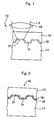
- the optical recording medium 10 is the write-once type medium. As shown in Fig. 1, this medium is composed of a substrate 12, a recording layer 18, and a light transmission layer 20 deposited in this order.
- the recording layer 18 is made of a mixture of a recording assist material and dielectric material.
- data recording/reproducing is performed by a laser beam LB irradiated from the side of the light transmission layer 20.
- the substrate 12 works as a base structure that provides a mechanical rigidity required of the optical recording medium 10.
- Grooves 22 and/or lands 24 are formed on the substrate surface. These grooves 22 and lands 24 work as guide tracks for the laser beam during data recording/reproducing.
- the substrate 12 is about 1.1mm thick and can be made of various materials such as glass, ceramics, and resin.
- Resin is a preferable material in terms of moldability.
- examples of such resin include polycarbonate resin, acryl resin, epoxy resin, polystyrene resin, polyethylene resin, polypropylene resin, silicone resin, fluoride-based resin, ABS resin, and urethane resin.
- polycarbonate resin is preferable in terms of processability.
- the dielectric material contains a state-change material as the base material. Optical characteristics including reflectivity of this material are varied due to energy by laser irradiation or the like.
- the dielectric material as the base material may be any material as long as it can cause a state change. Its principle component can be, for example, oxides, sulfides, nitrides, or their combination. More specifically, its principle component should be at least one dielectric material selected from the group consisting of Al 2 O 3 , AlN, ZnS, GeN, GeCrN, CeO 2 , SiO, SiO 2 , Ta 2 O 5 , SiC, MgO, MgF, LaSiON, Si 3 N 4 , TiO 2 and InSnO. A dielectric material comprising ZnS-SiO 2 as principle components is particularly preferable.
- the thickness of the recording layer 18 is not limited, the thickness is preferably 3-200nm. If it is thinner than 3nm, a sufficient change in the optical characteristics such as reflectivity of the entire layer does not occur even when the base material in the dielectric material has caused a sufficient change of state, and a sufficiently high C/N ratio is not provided. Meanwhile, if the layer is thicker than 200nm, the time for film deposition becomes long and the productivity may decrease, more heat becomes necessary to cause a change in the state of the base material in the dielectric material, and cracks are likely to be produced because of stress in the dielectric material.
- the recording assist material is a material that accelerates the reactions in the base material, and is mixed with the dielectric material as described above.
- the elements of the recording assist material receive the heat of the laser beam and then work on the dielectric material.
- the dielectric material causes a state change in whole or in part (for example, from amorphous to crystalline) to provide recording marks.
- This change of state may accompany a change of state (crystal growth) specific to a material contained in the recording assist material. This change of state will lead to improved C/N.
- the optical behavior against reproducing light significantly differ between the portion where recording marks have been formed and the other portion without recording marks.
- data recording/reproducing can be conducted based on such difference. This state can be confirmed by the X-ray diffraction or transmission electron microscopy.
- the recording assist material has at least one element selected from the group consisting of Sn, Ti, Si, Bi, Ge, C, V, W, Zr, Zn, Mg, Mn, Al, Nb, Au, Cu, Ta and Ag as a principle component.
- the principle component should account for 50% or more in the elements constituting the recording assist material, preferably 80 atomic percent (at%).
- the major element should account for 80 at% or more.
- the light transmission layer 20 is the layer working as the laser beam incident face and as a light path for the laser beam. Its thickness should be 10-300 ⁇ m, more preferably 50-150 ⁇ m.
- the material for the light transmission layer 20 is not limited, but acryl- or epoxy-based ultraviolet-curable resin is preferable. Instead of using an ultraviolet-curable resin film, a transparent sheet made of a transparent resin may be combined with glues and adhesives to form the light transmission layer 20.
- the recording layer 18 is formed on the substrate 12 where grooves 22 and lands 24 have been formed in advance.
- a vapor growth method using chemical species containing elements constituting the second dielectric layer 16B can be adopted.
- Such a vapor growth method may be the vacuum deposition method and sputtering method.
- chemical species where a dielectric material and a recording assist material are mixed may be employed in combination or separately.
- the light transmission layer 20 is formed on the recording layer 18.
- the light transmission layer 20 can be formed by, for example, the spin coating method that uses acryl- or epoxy-based ultraviolet-curable resin of which viscosity has been optimized in advance and cures this resin film by ultraviolet irradiation. Then the manufacturing of the optical recording medium is completed.
- the method of manufacturing the optical recording medium is not limited to the above example, but various techniques for manufacturing well-known optical recording media can be employed as well.
- Laser beam LB of a predetermined output power is irradiated onto the optical recording medium 10.
- the laser beam comes in the light transmission layer 20 and reaches the recording layer 18.
- NA numerical aperture
- the numerical aperture (NA) of the object lens that focuses laser beam LB should be 0.7 or higher, particularly 0.85 or so.
- the wavelength, ⁇ , of laser beam LB should be 450nm or shorter, particularly 405nm or so. Then, it is preferable to make ⁇ /NA ⁇ 640nm.
- the recording assist material constituting the recording layer 18 is heated by laser beam LB and recording assist material work on the adjacent dielectric material, accelerating the state change (for example, change from amorphous to crystalline), to form recording marks therein.
- crystal growth may occur in the recording assist material itself, and the extent of this crystallization may be larger than that of the dielectric material.
- the optical characteristics of the portion where recording marks have been formed are distinctively different from those of the other portion (non-recorded portion). Therefore, when a laser beam for mark reproducing is irradiated onto these recorded portion and the non-recorded portion, their reflectivities differ from each other and thereby the recorded data can be read. In other words, data can be recorded/read through modification of the optical characteristics.
- the recording layer 18 is made of a single layer.
- the present invention is not limited to this structure.
- the state-change assisting layer may be made of two or more layers if the same effect as above can be provided.
- the above optical recording medium 10 does not have a reflection layer on the substrate 12.
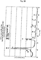
- a reflection layer 32 may be formed as in the case of the optical recording medium 30 shown in Fig. 2.
- the reflection layer 32 reflects the laser beam coming in from the side of the light transmission layer 20 and reflects it therethrough. Its thickness should be 5-300nm, preferably 10-200nm.
- the material for the reflection layer 52 is not particularly limited as long as it can reflect laser beams; for example, it can be Mg, Al, Ti, Cr, Fe, Co, Ni, Cu, Zn, Ge, Ag, Pt or Au. Because of high reflectivity, metallic materials such as Al, Au, Ag, or Cu, or their alloys (for example, Ag-Cu alloy) are particularly preferable. If the reflection layer 32 is formed, a high signal restoring ratio (C/N ratio) is easily attained after optical recording by virtue of the multi-interference effect.
- Optical recording media were fabricated via the following steps.
- a polycarbonate substrate of which thickness was 1.1mm and diameter was 120mm was set in a sputtering apparatus.
- a recording layer having a thickness of 10nm was formed by simultaneously sputtering the dielectric material made of a mixture of ZnS and SiO 2 and the recording assist material made of Sn. It was designed to have the recording assist material and ZnS-SiO 2 (80:20) at a molar ratio of 50:50.
- an acrylic ultraviolet-curable resin was coated by the spin coating method and the light transmission layer (thickness: 100 ⁇ m) was formed by ultraviolet irradiation thereon.
- Examples 2 and 3 were prepared in the same manner as in the example 1 except that Sn in the example 1 was replaced by Ag and Ti, respectively.
- an optical recording medium was fabricated to have a single-layered structure where the recording layer was made of only Sn.
- the optical recording medium with a recording layer of a single-layer structure was fabricated without forming any dielectric layer.
- Mg (examples 13-17), Ti (examples 18-25), Sn (examples 26,27), Nb (examples 28-30), or Al (examples 31-34) was mixed in the optical recording medium.
- the optical recording medium with a recording layer of a single-layer structure was fabricated without forming any dielectric layer.
- the recording layer was made of a mixture of Zn and other materials.
- the other materials are ZnS, ZnO and ZnS:SiO 2 (80:20) .
- optical recording media were each set in an optical disk tester (trade name: DDU1000 manufactured by Pulstec Industrial Co., Ltd.).
- a recording laser beam having a wavelength of 405nm (blue) and an object lens with an NA (numerical aperture) of 0.85 were employed in the individual optical recording media in common. This laser beam was focused with a focusing lens installed in the recording head and then irradiated from the light transmission layer side onto the optical recording medium for optical recording.
- the conditions for signal recording were that the modulation mode was (1, 7) RLL, the channel bit length was 0.12 ⁇ m, the linear recording rate was 5.3m/s, the channel clock was 66MHz, and the recorded signals were 8T.
- the information recorded with the aforementioned optical disk tester was reproduced and the C/N ratio of read signals was measured for each of the optical recording media fabricated in the individual examples and compared examples of different recording assist material and dielectric material constituting the recording layer and of different thicknesses of the entire recording layer.
- the wavelength of the laser beam used in reproduction was 405nm
- the NA (numerical aperture) of the object lens was 0.85
- the laser beam output power was 0.3mW.
- Example 1 Example 2 Film structure Recording layer Reflection layer Sn+80:20(10nm) Ag+80:20(10nm) 8T C/N(dB) 51.1 43.4
- Example 3 Compared example 1 Film structure Recording layer Reflection layer Ti+80:20(30nm) Sn(6nm) 8T C/N(dB) 51.2 29.1
- 80:20 means the molar ratio of ZnS:SiO 2 in ZnS+SiO 2 . Notation "ZnS:SiO 2 " is omitted in the table.
- Figure in () indicates the thickness of the entire recording layer.
- Example 4 Film structure Recording layer Reflection layer 80:20+Mg (30nm) 80:20+Nb (50nm) 80:20+Bi (10nm) 8T C/N (dB) 55.7 50.2 51.2
- Example 7 Example 8
- Example 10 Example 11
- Example 12 Film structure Recording layer Reflection layer 80:20+Cu (15nm) 80:20+Ta (20nm) 80:20+Si (40nm) 8T C/N (dB) 49.5 46.6 48.6
- 80:20 means the molar ratio of ZnS:SiO 2 in ZnS+SiO 2 .
- Example 18 Example 19 Example 20 Film structure Recording layer Reflection layer Si3N4+Ti(50nm) ZnS+Ti(30nm) TiO2+Ti(30nm) 8T C/N (dB) 42.3 50.1 48.3 Example 21
- Example 22 Example 23 Film structure Recording layer Reflection layer SiO2+Ti(50nm) SiC+Ti(30nm) 80:20+Ti(10nm) 8T C/N (dB) 44.7 51.6 51.2
- Example 24 Example 25 Film structure Recording layer Reflection layer 50:50+Ti(10nm Ta2O5+Ti(35nm 8T C/N (dB) 45.4 48.5 "80:20” and "50:50” mean the molar ratio of ZnS:SiO 2 in ZnS+SiO 2 .
- ZnS :SiO 2 is omitted in the table.
- Figure in () indicates the thickness of the entire recording layer.
- Table 6 Example 35
- Example 36 Example 37 Film structure Recording layer ZnS+Zn (30nm) ZnO+Zn (30nm) 80:20+Zn (30nm) 8T C/N (dB) 47 48.2 49.5 "80:20” means the molar ratio of ZnS:SiO 2 in ZnS+SiO 2.
- ZnS:SiO 2 is omitted in the table.
- Figure in () indicates the thickness of the entire recording layer.
- the recorded portion and non-recorded portion of the structure of mixture of ZnS-SiO 2 (80:20) and Sn(10nm) was analyzed by the X-ray diffraction. Before recording, crystals of Sn is recognized. After recording, crystals of both of ZnS and Sn observed. And crystallization of ZnS and Sn are recognized with a transmission electron scope.
- the X-ray was Cu-K ⁇ , and the tube voltage and tube current were 50kV and 300mA, respectively.
- the JCPDS cards were used to identify the diffraction peaks. For example, ⁇ -Sn is numbered 04-0673 and the positions of its diffraction peaks are known with reference to the card.
- the optical recording/reproducing method and optical recording medium of the present invention enable to record/read data with a simple structure in a novel manner not adopted in the past while reducing environmental loads.
Landscapes
- Chemical & Material Sciences (AREA)
- Inorganic Chemistry (AREA)
- Optical Record Carriers And Manufacture Thereof (AREA)
- Thermal Transfer Or Thermal Recording In General (AREA)
- Optical Recording Or Reproduction (AREA)
Applications Claiming Priority (4)
| Application Number | Priority Date | Filing Date | Title |
|---|---|---|---|
| JP2002162116 | 2002-06-03 | ||
| JP2002162116 | 2002-06-03 | ||
| JP2003035067 | 2003-02-13 | ||
| JP2003035067 | 2003-02-13 |
Publications (2)
| Publication Number | Publication Date |
|---|---|
| EP1403857A2 true EP1403857A2 (fr) | 2004-03-31 |
| EP1403857A3 EP1403857A3 (fr) | 2007-03-07 |
Family
ID=29738317
Family Applications (1)
| Application Number | Title | Priority Date | Filing Date |
|---|---|---|---|
| EP03012150A Withdrawn EP1403857A3 (fr) | 2002-06-03 | 2003-06-02 | Procédé d'enregistrement/lecture optique et support d'enregistrement optique |
Country Status (6)
| Country | Link |
|---|---|
| US (1) | US7136343B2 (fr) |
| EP (1) | EP1403857A3 (fr) |
| JP (1) | JP2004296056A (fr) |
| KR (1) | KR100678301B1 (fr) |
| CN (1) | CN1469362A (fr) |
| TW (1) | TWI256629B (fr) |
Families Citing this family (10)
| Publication number | Priority date | Publication date | Assignee | Title |
|---|---|---|---|---|
| US7235501B2 (en) | 2004-12-13 | 2007-06-26 | Micron Technology, Inc. | Lanthanum hafnium oxide dielectrics |
| US7560395B2 (en) | 2005-01-05 | 2009-07-14 | Micron Technology, Inc. | Atomic layer deposited hafnium tantalum oxide dielectrics |
| US7410910B2 (en) | 2005-08-31 | 2008-08-12 | Micron Technology, Inc. | Lanthanum aluminum oxynitride dielectric films |
| US7972974B2 (en) | 2006-01-10 | 2011-07-05 | Micron Technology, Inc. | Gallium lanthanide oxide films |
| US7759747B2 (en) | 2006-08-31 | 2010-07-20 | Micron Technology, Inc. | Tantalum aluminum oxynitride high-κ dielectric |
| US7776765B2 (en) | 2006-08-31 | 2010-08-17 | Micron Technology, Inc. | Tantalum silicon oxynitride high-k dielectrics and metal gates |
| US7432548B2 (en) | 2006-08-31 | 2008-10-07 | Micron Technology, Inc. | Silicon lanthanide oxynitride films |
| US7563730B2 (en) | 2006-08-31 | 2009-07-21 | Micron Technology, Inc. | Hafnium lanthanide oxynitride films |
| US7605030B2 (en) | 2006-08-31 | 2009-10-20 | Micron Technology, Inc. | Hafnium tantalum oxynitride high-k dielectric and metal gates |
| US7544604B2 (en) | 2006-08-31 | 2009-06-09 | Micron Technology, Inc. | Tantalum lanthanide oxynitride films |
Family Cites Families (5)
| Publication number | Priority date | Publication date | Assignee | Title |
|---|---|---|---|---|
| JPS57205193A (en) * | 1981-06-12 | 1982-12-16 | Fuji Photo Film Co Ltd | Optical information recording medium |
| KR890004230B1 (ko) * | 1984-08-24 | 1989-10-27 | 가부시끼가이샤 도오시바 | 광(光) 디스크 메모리 |
| JPS62204442A (ja) | 1986-03-03 | 1987-09-09 | Toshiba Corp | 光記録媒体および光記録媒体の記録方法 |
| US5635267A (en) * | 1992-09-17 | 1997-06-03 | Matsushita Electric Industrial Co., Ltd. | Optical information recording medium of phase change type having variably grooved tracks depending on their radial locations |
| TW484126B (en) * | 1999-03-26 | 2002-04-21 | Matsushita Electric Industrial Co Ltd | Manufacturing and recording regeneration method for information record medium |
-
2003
- 2003-05-20 TW TW092113636A patent/TWI256629B/zh not_active IP Right Cessation
- 2003-05-29 US US10/447,109 patent/US7136343B2/en not_active Expired - Lifetime
- 2003-05-30 KR KR1020030034739A patent/KR100678301B1/ko not_active Expired - Fee Related
- 2003-06-02 JP JP2003156562A patent/JP2004296056A/ja active Pending
- 2003-06-02 EP EP03012150A patent/EP1403857A3/fr not_active Withdrawn
- 2003-06-03 CN CNA031379958A patent/CN1469362A/zh active Pending
Also Published As
| Publication number | Publication date |
|---|---|
| CN1469362A (zh) | 2004-01-21 |
| TWI256629B (en) | 2006-06-11 |
| KR20030094051A (ko) | 2003-12-11 |
| TW200307925A (en) | 2003-12-16 |
| US20030235134A1 (en) | 2003-12-25 |
| KR100678301B1 (ko) | 2007-02-01 |
| JP2004296056A (ja) | 2004-10-21 |
| US7136343B2 (en) | 2006-11-14 |
| EP1403857A3 (fr) | 2007-03-07 |
Similar Documents
| Publication | Publication Date | Title |
|---|---|---|
| US20070190460A1 (en) | Optical recording/reproducing method | |
| US20040157158A1 (en) | Optical recording medium | |
| KR100734641B1 (ko) | 광기록매체, 광기록/재생장치, 광기록장치 및 광재생장치,광기록매체용 데이터 기록/재생 방법 및 데이터 기록방법및 데이터 재생 방법 | |
| US6929840B2 (en) | Optical recording medium, method for manufacturing the same and target used for sputtering process | |
| US7018695B2 (en) | Optical recording medium | |
| KR20040063839A (ko) | 광기록 매체 | |
| EP1398767B1 (fr) | Procédé d'enregistrement/lecture optique et support d'enregistrement optique | |
| US7601481B2 (en) | Multilayer phase-change information recording medium, and method for recording and reproducing using the same | |
| EP1403857A2 (fr) | Procédé d'enregistrement/lecture optique et support d'enregistrement optique | |
| JPWO2004032130A1 (ja) | 光学的情報記録媒体とその製造方法 | |
| WO2002043060A1 (fr) | Moyen d'enregistrement optique | |
| EP1400960A2 (fr) | Procédé d'enregistrement/lecture optique et support d'enregistrement optique | |
| JP5298623B2 (ja) | 追記型光記録媒体 | |
| JP4251142B2 (ja) | 追記型光記録媒体 | |
| JP4322719B2 (ja) | 光情報記録媒体及びその製造方法とスパッタリングターゲット | |
| JP2007141417A (ja) | 追記型光記録媒体およびその製造方法 | |
| JP4232159B2 (ja) | 光記録媒体 | |
| JP2005243218A (ja) | 光記録媒体 | |
| US20060165944A1 (en) | Optical recording medium | |
| JP2004342196A (ja) | 追記型光記録媒体とその記録方法 | |
| JP2005203072A (ja) | 光記録媒体 | |
| JP2004296057A (ja) | 光記録再生方法及び光記録媒体 |
Legal Events
| Date | Code | Title | Description |
|---|---|---|---|
| PUAI | Public reference made under article 153(3) epc to a published international application that has entered the european phase |
Free format text: ORIGINAL CODE: 0009012 |
|
| AK | Designated contracting states |
Kind code of ref document: A2 Designated state(s): AT BE BG CH CY CZ DE DK EE ES FI FR GB GR HU IE IT LI LU MC NL PT RO SE SI SK TR |
|
| AX | Request for extension of the european patent |
Extension state: AL LT LV MK |
|
| PUAL | Search report despatched |
Free format text: ORIGINAL CODE: 0009013 |
|
| STAA | Information on the status of an ep patent application or granted ep patent |
Free format text: STATUS: THE APPLICATION HAS BEEN WITHDRAWN |
|
| AK | Designated contracting states |
Kind code of ref document: A3 Designated state(s): AT BE BG CH CY CZ DE DK EE ES FI FR GB GR HU IE IT LI LU MC NL PT RO SE SI SK TR |
|
| AX | Request for extension of the european patent |
Extension state: AL LT LV MK |
|
| 18W | Application withdrawn |
Effective date: 20070209 |