EP1403973A2 - Connecteur pour un module - Google Patents
Connecteur pour un module Download PDFInfo
- Publication number
- EP1403973A2 EP1403973A2 EP03017369A EP03017369A EP1403973A2 EP 1403973 A2 EP1403973 A2 EP 1403973A2 EP 03017369 A EP03017369 A EP 03017369A EP 03017369 A EP03017369 A EP 03017369A EP 1403973 A2 EP1403973 A2 EP 1403973A2
- Authority
- EP
- European Patent Office
- Prior art keywords
- connector
- contact
- camera module
- chamber
- module body
- Prior art date
- Legal status (The legal status is an assumption and is not a legal conclusion. Google has not performed a legal analysis and makes no representation as to the accuracy of the status listed.)
- Withdrawn
Links
- 238000010276 construction Methods 0.000 description 3
- 230000001413 cellular effect Effects 0.000 description 2
- 238000003780 insertion Methods 0.000 description 2
- 230000037431 insertion Effects 0.000 description 2
- 238000012986 modification Methods 0.000 description 2
- 230000004048 modification Effects 0.000 description 2
Images



Classifications
-
- H—ELECTRICITY
- H01—ELECTRIC ELEMENTS
- H01R—ELECTRICALLY-CONDUCTIVE CONNECTIONS; STRUCTURAL ASSOCIATIONS OF A PLURALITY OF MUTUALLY-INSULATED ELECTRICAL CONNECTING ELEMENTS; COUPLING DEVICES; CURRENT COLLECTORS
- H01R13/00—Details of coupling devices of the kinds covered by groups H01R12/70 or H01R24/00 - H01R33/00
- H01R13/46—Bases; Cases
- H01R13/514—Bases; Cases composed as a modular blocks or assembly, i.e. composed of co-operating parts provided with contact members or holding contact members between them
-
- H—ELECTRICITY
- H01—ELECTRIC ELEMENTS
- H01R—ELECTRICALLY-CONDUCTIVE CONNECTIONS; STRUCTURAL ASSOCIATIONS OF A PLURALITY OF MUTUALLY-INSULATED ELECTRICAL CONNECTING ELEMENTS; COUPLING DEVICES; CURRENT COLLECTORS
- H01R12/00—Structural associations of a plurality of mutually-insulated electrical connecting elements, specially adapted for printed circuits, e.g. printed circuit boards [PCB], flat or ribbon cables, or like generally planar structures, e.g. terminal strips, terminal blocks; Coupling devices specially adapted for printed circuits, flat or ribbon cables, or like generally planar structures; Terminals specially adapted for contact with, or insertion into, printed circuits, flat or ribbon cables, or like generally planar structures
- H01R12/70—Coupling devices
- H01R12/71—Coupling devices for rigid printing circuits or like structures
- H01R12/712—Coupling devices for rigid printing circuits or like structures co-operating with the surface of the printed circuit or with a coupling device exclusively provided on the surface of the printed circuit
- H01R12/716—Coupling device provided on the PCB
-
- H—ELECTRICITY
- H05—ELECTRIC TECHNIQUES NOT OTHERWISE PROVIDED FOR
- H05K—PRINTED CIRCUITS; CASINGS OR CONSTRUCTIONAL DETAILS OF ELECTRIC APPARATUS; MANUFACTURE OF ASSEMBLAGES OF ELECTRICAL COMPONENTS
- H05K7/00—Constructional details common to different types of electric apparatus
- H05K7/02—Arrangements of circuit components or wiring on supporting structure
- H05K7/10—Plug-in assemblages of components, e.g. IC sockets
- H05K7/1015—Plug-in assemblages of components, e.g. IC sockets having exterior leads
- H05K7/103—Plug-in assemblages of components, e.g. IC sockets having exterior leads co-operating by sliding, e.g. DIP carriers
- H05K7/1046—J-shaped leads
-
- H—ELECTRICITY
- H05—ELECTRIC TECHNIQUES NOT OTHERWISE PROVIDED FOR
- H05K—PRINTED CIRCUITS; CASINGS OR CONSTRUCTIONAL DETAILS OF ELECTRIC APPARATUS; MANUFACTURE OF ASSEMBLAGES OF ELECTRICAL COMPONENTS
- H05K7/00—Constructional details common to different types of electric apparatus
- H05K7/02—Arrangements of circuit components or wiring on supporting structure
- H05K7/10—Plug-in assemblages of components, e.g. IC sockets
- H05K7/1053—Plug-in assemblages of components, e.g. IC sockets having interior leads
- H05K7/1061—Plug-in assemblages of components, e.g. IC sockets having interior leads co-operating by abutting
- H05K7/1069—Plug-in assemblages of components, e.g. IC sockets having interior leads co-operating by abutting with spring contact pieces
Definitions
- This invention relates to a connector to which a module such as a memory module and a camera module is fitted.
- Figs. 4A to 4C show a first related-art camera module 1 to be mounted on a cellular mobile phone or the like, and this camera module 1 comprises a module body 2, and a lens portion 3 formed on an upper side of the module body 2. Two (left and right) rows of contact pads 4 and 5 are formed on a bottom face of the module body 2.
- Figs. 5A to 5D show a related-art connector 6 to which the camera module 1 is fitted.
- the connector 6 is formed into a square box-like body having an upwardly-open chamber 6a.
- Two (left and right) rows of parallel grooves 7 and 8 are formed in an upper face of a bottom 6b of the chamber 6a, so that the left grooves 7 extend from a central portion of the bottom 6b to an inner left side wall of the chamber 6a, and the right grooves 8 extend from the central portion of the bottom 6b to an inner right side wall of the chamber 6a.
- a row of left contact pins 9 are provided in the left grooves 7, respectively, while a row of right contact pins 10 are provided in the right grooves 8, respectively.
- each of the left row of contact pins 9 is bent upwardly to project from an associated groove 7 to form a contact projection 9a for contact with an associated contact pad 4 of the camera module 1.
- Each contact pin 9 extends left, and passes through the connector 6 to project to the exterior, and an outer end portion of the contact pin 9 is bent to form a terminal 9b for contact with a wiring board (not shown) on which the connector 6 is mounted.
- each of the right row of contact pins 10 is bent upwardly to project from an associated groove 7 to form a contact projection 10a for contact with an associated contact pad 5 of the camera module 1.
- Each contact pin 10 extends right, and passes through the connector 6 to project to the exterior, and an outer end portion of the contact pin 10 is bent to form a terminal 10b for contact with the wiring board
- the contact pins 9 and 10 are bent as indicated in phantom lines in Fig. 5D, so that the distal ends (inner ends) of the contact pins 9 and 10 abut against the bottom of the grooves 7 and 8.
- the contact pins 9 and 10 are accordingly held in firm press-contact respectively with the contact pads 4 and 5 because of reaction forces of these contact pins.
- Signals of the camera module 1 are transmitted to the contact pins 9 and 10 via the contact pads 4 and 5 and the contact projections 9a and 10a, and further are transmitted to a circuit (not shown) of the wiring board via the terminals 9b and 10b.
- Figs. 7A to 7D show a second related-art camera module 11.
- This camera module 11 comprises a module body 12, and a lens portion 13 formed on an upper side of the module body 12.
- a projection 14 is extended horizontally from one side face of the module body 12.
- a plurality of parallel contacts 15 are provided on an upper face of the projection 14, while a plurality of parallel contacts 16 are provided on a lower face of the projection 14.
- Figs. 8A to 8D show a connector 17 to which the camera module 11 is attached.
- This connector 17 is formed into a box-like body having an open chamber 17a.
- a central portion of a left half portion of the upper side of this connector is open, and a row of upper contact pins 18 and a row of lower contact pins 19 for gripping the contact portions 15 and 16 (provided on the projection 14 of the module body 12) are provided at an inner bottom portion of the connector 17 disposed on the right side of the chamber 17a.
- each of the contact pins 18, disposed near to the central portion of the connector 17, is bent to form a contact projection 18a for contact with the associated contact portion 15 of the module body 12, and an inner end portion of each of the contact pins 19, disposed near to the central portion of the connector 17, is bent to form a contact projection 19a for contact with the associated contact portion 16 of the module body 12.
- the contact pins 18 and 19 extend so as to pass through the connector 17 to project to the exterior, so that an outer end portion of each contact pin 18 is bent to form a terminal portion 18b for contact with a wiring board (not shown) on which the connector 17 is mounted, and an outer end portion of each contact pin 19 is bent to form a terminal portion 19b for contact with the wiring board.
- the projection 14 of the camera module 11 is held between the contact pins 18 and the contact pins 19 in such a manner that the contact portions 15 and 16 are held in press-contact with the contact projections 18a and 19a of the contact pins 18 and 19, respectively.
- the camera module 11 is attached to the connector 17 as shown in Fig. 9.
- the connector 6 has an increased height H1, and also an overall height H2, obtained when attaching the camera module 1 to the connector 6, is increased, and these are causes of the failure to achieve a thinner design of the connector 6 and a thinner design of the structure obtained by attaching the camera module 1 to the connector 6.
- a height H3 of the connector 17 is hardly increased, and also an overall height H4, obtained when attaching the camera module 11 to the connector 17, is hardly increased, and therefore a thinner design can be achieved.
- the camera module 11 has the projection 14 formed on the side face thereof, and therefore a width L1 of the camera module 11 is increased, and also the connector 17 has an increased width L2 since the connector 17 includes the portion for receiving the body portion 12 of the camera module 11 and the portion for contact with the projection 14.
- a width of the overall structure, obtained by attaching the camera module 11 to the connector 17, has the dimension L2. Therefore, there is encountered a problem that a space saving design can not be achieved.
- connection structure comprising:
- the height of the connector can be made smaller, and also the height of the overall structure, obtained by attaching the module body to the connector, can be made smaller, thereby achieving the thinner design. Further, the width of the connector can be made smaller, and the space-saving design can be achieved.
- the second conductive member is extended in a direction parallel to an inserting direction of the module body.
- the module body is a memory module or a camera module.
- an end of the chamber opposite to the opening is made open.
- a bottom wall of the chamber as provided in the related-art construction is not provided at the end of the chamber, so that the thickness of the connector can be further reduced.
- At least a pair of the second conductive member is arranged on the inner side face of the connector so as to oppose to each other.
- the second conductive member has elasticity.
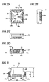
- Figs. 1A to 1D show a camera module 21 mounted on a cellular mobile phone or the like, and this camera module 21 comprises a module body 22, and a lens portion 23 formed on an upper side of the module body 22.
- a plurality of parallel contact pads 24 are formed at a lower half portion of each of four side faces of the module body 22, and extend vertically.
- FIGs. 2A to 2D show a connector 25 to which the camera module 21 is fitted.
- This connector 25 is formed into a square box-like body having an upwardly-open chamber 25a.
- Four side portions of a bottom 25b of the chamber 25a are suitably notched to form openings 25c, and a plurality of parallel contact pins 26 are provided on an inner side wall of the chamber 25a, and extend vertically.
- the connector 25 has the bottom 25b, this bottom 25b may be removed so as to provide the chamber 25a having an open top and an open bottom.
- the connector 25 is reduced in thickness by an amount corresponding to the thickness of this removed bottom wall 25b.
- Each of the contact pins 26 is bent into a generally inverted V-shape, and is fixedly secured to the inner side face of the chamber 25a.
- One end portion of the contact pin 26 is formed into a terminal 26a which is exposed to the lower side of the connector 25 through the associated opening 25c, and is bent outwardly horizontally so as to be electrically connected with a circuit (not shown) formed on a wiring board (not shown) on which the connector 25 is mounted.
- the other end portion of the contact pin 26 is bent to project inwardly to form a contact projection 26b for contact with the associated contact pad 24 of the module body 22.
- Signals of the camera module 21 are transmitted from the contact pads 24 to the contact pins 26 via the contact projections 26b, and further are transmitted to the circuit of the wiring board via the terminals 26a.
- a height H5 of the connector 25 can be made smaller, and also a height H6 of the overall structure, obtained by attaching the camera module 21 to the connector 25, can be made smaller, thereby achieving a thinner design.
- a width L3 of the connector can be made smaller as compared with the second related-art connector shown in Fig. 9, thereby achieving a space-saving design.
- the contact pins 26 of the connector 25 are pressed against the contact pads 24 of the camera module 21, respectively, in a gripping manner, the stable contact can be obtained. Furthermore, since a force, exerted in the direction of insertion of the camera module 21, is not applied directly to the contact pins 26, there is achieved an advantage that the contact pins 26 will not be damaged.
- the connector 25 is so designed as to attach the camera module 21 thereto
- the connector of the invention is not limited to the type for attaching the camera module thereto, but the invention can be applied to connectors for attaching various modules (such for example as a memory module) or electric parts thereto.
Landscapes
- Engineering & Computer Science (AREA)
- Microelectronics & Electronic Packaging (AREA)
- Coupling Device And Connection With Printed Circuit (AREA)
- Studio Devices (AREA)
- Connecting Device With Holders (AREA)
- Connector Housings Or Holding Contact Members (AREA)
Applications Claiming Priority (2)
| Application Number | Priority Date | Filing Date | Title |
|---|---|---|---|
| JP2002222942 | 2002-07-31 | ||
| JP2002222942A JP2004063391A (ja) | 2002-07-31 | 2002-07-31 | モジュール用コネクタ |
Publications (2)
| Publication Number | Publication Date |
|---|---|
| EP1403973A2 true EP1403973A2 (fr) | 2004-03-31 |
| EP1403973A3 EP1403973A3 (fr) | 2006-04-19 |
Family
ID=31184941
Family Applications (1)
| Application Number | Title | Priority Date | Filing Date |
|---|---|---|---|
| EP03017369A Withdrawn EP1403973A3 (fr) | 2002-07-31 | 2003-07-31 | Connecteur pour un module |
Country Status (4)
| Country | Link |
|---|---|
| US (2) | US7077663B2 (fr) |
| EP (1) | EP1403973A3 (fr) |
| JP (1) | JP2004063391A (fr) |
| KR (1) | KR20040012515A (fr) |
Families Citing this family (20)
| Publication number | Priority date | Publication date | Assignee | Title |
|---|---|---|---|---|
| EP1596427A4 (fr) | 2003-02-19 | 2009-06-10 | Panasonic Corp | Procede d'introduction d'impuretes |
| JP3956920B2 (ja) * | 2003-08-26 | 2007-08-08 | 松下電工株式会社 | コネクタ |
| JP2005222876A (ja) | 2004-02-09 | 2005-08-18 | Smk Corp | モジュール用コネクタ |
| US7495702B2 (en) * | 2004-02-09 | 2009-02-24 | Nokia Corporation | Portable electronic device with camera |
| JP2005339830A (ja) * | 2004-05-24 | 2005-12-08 | Alps Electric Co Ltd | 電気部品用ソケット装置 |
| JP4100694B2 (ja) * | 2004-05-31 | 2008-06-11 | 日本航空電子工業株式会社 | コネクタ |
| JP4515215B2 (ja) * | 2004-10-07 | 2010-07-28 | モレックス インコーポレイテド | ソケット |
| CN2757364Y (zh) * | 2004-11-18 | 2006-02-08 | 富士康(昆山)电脑接插件有限公司 | 电连接器 |
| JP4562538B2 (ja) * | 2005-01-31 | 2010-10-13 | モレックス インコーポレイテド | モジュール用ソケット |
| US20060189216A1 (en) * | 2005-02-18 | 2006-08-24 | Ming-Hsun Yang | Camera module connector keying structure |
| TWM271287U (en) * | 2005-02-18 | 2005-07-21 | Molex Taiwan Ltd | Camera module connector |
| CN2800590Y (zh) * | 2005-05-31 | 2006-07-26 | 富士康(昆山)电脑接插件有限公司 | 电连接器 |
| TWM304793U (en) * | 2006-04-03 | 2007-01-11 | Hon Hai Prec Ind Co Ltd | Electrical connector assembly |
| CN200941518Y (zh) * | 2006-08-01 | 2007-08-29 | 富士康(昆山)电脑接插件有限公司 | 电连接器 |
| JP3136253U (ja) * | 2006-08-18 | 2007-10-18 | 鴻海精密工業股▲ふん▼有限公司 | コネクタ |
| CN200941495Y (zh) * | 2006-08-18 | 2007-08-29 | 富士康(昆山)电脑接插件有限公司 | 电连接器 |
| TWM310502U (en) * | 2006-11-17 | 2007-04-21 | Molex Taiwan Ltd | Electrical connection device |
| US8079849B2 (en) * | 2010-05-11 | 2011-12-20 | Tyco Electronics Corporation | Socket connector assembly with compressive contacts |
| CN105684413A (zh) * | 2014-01-26 | 2016-06-15 | 华为终端有限公司 | 一种主板结构及终端 |
| CN108574159B (zh) * | 2017-03-10 | 2020-08-07 | 唐虞企业股份有限公司 | 连接器及其制造方法 |
Family Cites Families (15)
| Publication number | Priority date | Publication date | Assignee | Title |
|---|---|---|---|---|
| US3701077A (en) * | 1969-12-29 | 1972-10-24 | Tech Inc K | Electronic components |
| US4378139A (en) * | 1981-07-14 | 1983-03-29 | Wells Electronics, Inc. | Integrated circuit carrier connector |
| EP0404277B1 (fr) * | 1984-02-27 | 1994-09-28 | The Whitaker Corporation | Méthode d'insertion d'un contact de support de puce dans un boîtier |
| US4747017A (en) * | 1986-05-27 | 1988-05-24 | General Motors Corporation | Surface mountable integrated circuit package equipped with sockets |
| US4934944B1 (en) * | 1988-11-07 | 1994-07-19 | Methode Electronics Inc | Chip carrier socket with open aperture |
| US5055972A (en) * | 1990-01-23 | 1991-10-08 | Kel Corporation | Chip carrier socket |
| US5289034A (en) * | 1990-01-26 | 1994-02-22 | Sgs-Thomson Microelectronics, Inc. | IC package having replaceable backup battery |
| US5104327A (en) * | 1991-02-28 | 1992-04-14 | Amp Incorporated | Wire form socket connector |
| US5249971A (en) * | 1991-09-13 | 1993-10-05 | Foxconn International, Inc. | IC package connector |
| US5226824A (en) * | 1992-05-13 | 1993-07-13 | Foxconn International, Inc. | IC socket and contact therein |
| JPH0676894A (ja) * | 1992-08-28 | 1994-03-18 | Murata Mfg Co Ltd | コネクタ |
| US6268882B1 (en) * | 1998-12-31 | 2001-07-31 | Elbex Video Ltd. | Dome shaped camera with simplified construction and positioning |
| KR100355223B1 (ko) * | 1999-01-07 | 2002-10-09 | 삼성전자 주식회사 | 멀티 인라인 메모리 모듈 및 그와 결합되는 전자 부품 소켓 |
| US6435882B1 (en) * | 2001-07-27 | 2002-08-20 | Agilent Technologies, Inc. | Socketable flexible circuit based electronic device module and a socket for the same |
| US6328574B1 (en) * | 2001-07-27 | 2001-12-11 | Hon Hai Precision Ind. Co., Ltd. | High current capacity socket with side contacts |
-
2002
- 2002-07-31 JP JP2002222942A patent/JP2004063391A/ja active Pending
-
2003
- 2003-07-29 KR KR1020030052266A patent/KR20040012515A/ko not_active Ceased
- 2003-07-30 US US10/629,570 patent/US7077663B2/en not_active Expired - Fee Related
- 2003-07-31 EP EP03017369A patent/EP1403973A3/fr not_active Withdrawn
-
2006
- 2006-06-02 US US11/445,149 patent/US7163407B2/en not_active Expired - Fee Related
Also Published As
| Publication number | Publication date |
|---|---|
| KR20040012515A (ko) | 2004-02-11 |
| US7077663B2 (en) | 2006-07-18 |
| EP1403973A3 (fr) | 2006-04-19 |
| JP2004063391A (ja) | 2004-02-26 |
| US7163407B2 (en) | 2007-01-16 |
| US20060246751A1 (en) | 2006-11-02 |
| US20040023528A1 (en) | 2004-02-05 |
Similar Documents
| Publication | Publication Date | Title |
|---|---|---|
| US6905344B2 (en) | Module connector | |
| EP1403973A2 (fr) | Connecteur pour un module | |
| US6729890B2 (en) | Reduced-size board-to-board connector | |
| US4695115A (en) | Telephone connector with bypass capacitor | |
| CN101567494B (zh) | 用于将母线终端连接到印刷电路板的母线连接器 | |
| US6431893B1 (en) | Switch for an electrical card connector | |
| US7402078B2 (en) | Electrical connector with firm frame for mating with corresponding connector | |
| US6508665B1 (en) | Electrical connector having printed circuit board mounted therein | |
| JP3898643B2 (ja) | 小型基板対基板コネクタ | |
| JPH0748389B2 (ja) | 印刷回路板用高密度電気コネクタ | |
| US6168473B1 (en) | Clamping structure for communication connector | |
| US7540777B2 (en) | Plug-in connector for connecting electronic components | |
| US6210177B1 (en) | Electrical connector | |
| US6227907B1 (en) | Surface mounted electrical connector | |
| US7063571B2 (en) | Smart card connector | |
| US6736672B1 (en) | Stacked card connector having two rows of terminals extending out of a bottom surface of the connector at a side opposite to an insert port | |
| US7572151B2 (en) | Plug connector for mobile communication device | |
| US20040219805A1 (en) | Electric connector | |
| US6905345B2 (en) | Electrical connector assembly | |
| US6431883B2 (en) | Input/output connector for a mobile electric device | |
| US5722839A (en) | Electrical connector for horizontal insertion of a CPU module therein | |
| US7402079B2 (en) | Electrical connector | |
| JP3156557U (ja) | 導電端子、及びこれを用いた電気コネクタ | |
| US6290544B1 (en) | Electrical connector with adapter for increasing an overall height of the connector above a prited circuit borad | |
| KR100806358B1 (ko) | 이동통신단말기용 커넥터 플러그 |
Legal Events
| Date | Code | Title | Description |
|---|---|---|---|
| PUAI | Public reference made under article 153(3) epc to a published international application that has entered the european phase |
Free format text: ORIGINAL CODE: 0009012 |
|
| AK | Designated contracting states |
Kind code of ref document: A2 Designated state(s): AT BE BG CH CY CZ DE DK EE ES FI FR GB GR HU IE IT LI LU MC NL PT RO SE SI SK TR |
|
| AX | Request for extension of the european patent |
Extension state: AL LT LV MK |
|
| PUAL | Search report despatched |
Free format text: ORIGINAL CODE: 0009013 |
|
| AK | Designated contracting states |
Kind code of ref document: A3 Designated state(s): AT BE BG CH CY CZ DE DK EE ES FI FR GB GR HU IE IT LI LU MC NL PT RO SE SI SK TR |
|
| AX | Request for extension of the european patent |
Extension state: AL LT LV MK |
|
| RIC1 | Information provided on ipc code assigned before grant |
Ipc: H01R 12/18 20060101ALI20060228BHEP Ipc: H05K 7/10 20060101AFI20060228BHEP |
|
| 17P | Request for examination filed |
Effective date: 20060825 |
|
| AKX | Designation fees paid |
Designated state(s): DE FI FR |
|
| STAA | Information on the status of an ep patent application or granted ep patent |
Free format text: STATUS: THE APPLICATION HAS BEEN WITHDRAWN |
|
| 18W | Application withdrawn |
Effective date: 20100719 |