EP1404044A2 - Verbesserungen in und in Bezug auf die Detektion von analogen Wartungssignalen - Google Patents
Verbesserungen in und in Bezug auf die Detektion von analogen Wartungssignalen Download PDFInfo
- Publication number
- EP1404044A2 EP1404044A2 EP20030078002 EP03078002A EP1404044A2 EP 1404044 A2 EP1404044 A2 EP 1404044A2 EP 20030078002 EP20030078002 EP 20030078002 EP 03078002 A EP03078002 A EP 03078002A EP 1404044 A2 EP1404044 A2 EP 1404044A2
- Authority
- EP
- European Patent Office
- Prior art keywords
- signal
- optical
- frequency
- channel
- band
- Prior art date
- Legal status (The legal status is an assumption and is not a legal conclusion. Google has not performed a legal analysis and makes no representation as to the accuracy of the status listed.)
- Withdrawn
Links
Images








Classifications
-
- H—ELECTRICITY
- H04—ELECTRIC COMMUNICATION TECHNIQUE
- H04B—TRANSMISSION
- H04B10/00—Transmission systems employing electromagnetic waves other than radio-waves, e.g. infrared, visible or ultraviolet light, or employing corpuscular radiation, e.g. quantum communication
- H04B10/07—Arrangements for monitoring or testing transmission systems; Arrangements for fault measurement of transmission systems
- H04B10/075—Arrangements for monitoring or testing transmission systems; Arrangements for fault measurement of transmission systems using an in-service signal
- H04B10/077—Arrangements for monitoring or testing transmission systems; Arrangements for fault measurement of transmission systems using an in-service signal using a supervisory or additional signal
-
- H—ELECTRICITY
- H04—ELECTRIC COMMUNICATION TECHNIQUE
- H04B—TRANSMISSION
- H04B10/00—Transmission systems employing electromagnetic waves other than radio-waves, e.g. infrared, visible or ultraviolet light, or employing corpuscular radiation, e.g. quantum communication
- H04B10/25—Arrangements specific to fibre transmission
- H04B10/2507—Arrangements specific to fibre transmission for the reduction or elimination of distortion or dispersion
- H04B10/2537—Arrangements specific to fibre transmission for the reduction or elimination of distortion or dispersion due to scattering processes, e.g. Raman or Brillouin scattering
-
- H—ELECTRICITY
- H04—ELECTRIC COMMUNICATION TECHNIQUE
- H04J—MULTIPLEX COMMUNICATION
- H04J14/00—Optical multiplex systems
- H04J14/02—Wavelength-division multiplex systems
- H04J14/0298—Wavelength-division multiplex systems with sub-carrier multiplexing [SCM]
-
- H—ELECTRICITY
- H04—ELECTRIC COMMUNICATION TECHNIQUE
- H04B—TRANSMISSION
- H04B2210/00—Indexing scheme relating to optical transmission systems
- H04B2210/07—Monitoring an optical transmission system using a supervisory signal
- H04B2210/078—Monitoring an optical transmission system using a supervisory signal using a separate wavelength
-
- H—ELECTRICITY
- H04—ELECTRIC COMMUNICATION TECHNIQUE
- H04J—MULTIPLEX COMMUNICATION
- H04J14/00—Optical multiplex systems
- H04J14/02—Wavelength-division multiplex systems
- H04J14/0227—Operation, administration, maintenance or provisioning [OAMP] of WDM networks, e.g. media access, routing or wavelength allocation
Definitions
- the present invention relates to methods and apparatus suitable for the processing of optical signals modulated by low frequency signals such as analogue maintenance signals. Such methods and apparatus are suitable for, but not limited to, improving the detectability of analogue maintenance signals.
- Wavelength division multiplexing is the sending of signals of different wavelengths simultaneously along the same transmission medium (normally an optical fibre). Each of the separate wavelengths can carry a separate information signal, thus allowing the simultaneous transmission of a number of different signals.
- each wavelength utilised to carry an information signal is referred to as a channel.
- Information is carried within each channel by modulating the optical signal at a relatively high speed e.g. bit rates of 2.5Gb/s to 40Gb/s are common.
- Analogue maintenance is the application of a relatively low frequency tone (less than the information bit rate), at a relatively small amplitude to the optical signal.
- tones within the frequency range 300kHz to 400kHz may be used.
- Such a frequency is utilised to amplitude modulate the optical information signal at a relatively small modulation depth e.g. 1% of the peak power of the optical signal.
- Analogue maintenance signals can be utilised to carry signalling data, for instance indicative of the source of the relevant channel, or for control of the optical network.
- each channel within a WDM signal may be allocated a frequency band within the range 300kHz - 400kHz, each band covering eight separate frequencies separated by 32Hz.
- Signalling information can thus be transmitted by applying in turn different sequences of the eight frequencies to modulate the relevant optical signal.
- analogue maintenance signal As the analogue maintenance signal is applied at a predetermined proportion of the optical signal power, detection and determination of the amplitude of an analogue maintenance signal can be used to calculate the power in the relevant channel, thus easily allowing the monitoring of the performance of an optical link.
- Figure 1 shows an optical network 100, including a node 200.
- the node 200 includes apparatus for the detection of an analogue maintenance signal.
- the node 200 also includes a receiver 300 for detecting at least one of the information signals carried by a relevant channel.
- the receiver 300 will typically include a WDM demultiplexer, arranged to demultiplex the optical signal into individual channels. Each individual channel can then be detected by a photo detector.
- An optical signal comprising a number of channels, is received from the rest of the network 100 by the node 200. The majority of this signal is passed to the receiver 300. A predetermined proportion of the signal (typically 1% - 5%) is removed by optical tap 210, and passed to a photo detector 220, such as a photodiode. The photo detector converts the optical signal to an electrical signal. For convenience an amplifier 230 amplifies the electrical signal, the output voltage of the amplifier being passed to both a band pass filter 250 and a low pass filter 240.
- the low pass filter 240 is arranged to pass only very low frequency components of the electrical signal (e.g. signals less than 1kHz), with the resulting DC output voltage being indicative of the total power of the optical signal i.e. the sum of the powers within each channel.
- the band pass filter 250 is arranged to filter out both the DC component of the input signal, and the high frequency components (e.g. those frequencies corresponding to the bit-rate of the information signal), and hence to pass those frequencies corresponding to the analogue maintenance signals.
- the band pass filter may be arranged to pass frequencies within the range 1kHz to 1MHz.
- the signal passed by the band pass filter will thus contain frequency signals corresponding to each of the analogue maintenance signals for each channel.
- the relative powers of each channel within the optical signal can be determined (as the power of a maintenance signal is a predetermined proportion of the total signal power).
- the total power of the optical signal can be determined from the output of the low pass filter 240, consequently the optical power per channel can be determined. Further, by analysing the exact frequency present at any given instance, the signal information carried by the analogue maintenance signal can be determined.
- the output of the band pass filter 250 is passed to an analogue to digital converter 260, which digitizes the signal.
- the resulting digital signal is passed to a digital signal processor 270, which can determine both the frequency components and amplitudes of the frequency components present.
- Stimulated Raman Scattering results in the transfer of optical power between different wavelengths of optical signal being transmitted simultaneously along a transmission medium such as optical fibre.
- the power transferred between the different wavelengths is a function of the instantaneous channel powers.
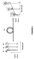
- Figure 2 illustrates the Raman gain coefficients for a typical optical fibre in relation to a pump signal at 1530nm.
- the solid line indicates the actual Raman gain coefficient, with the dotted line indicating an approximation of the Raman gain coefficient g that can be used to simplify the Raman power transfer calculation.
- the Raman gain coefficient within this range increases with increasing wavelength.
- an optical signal incorporating two or more channels at separate wavelength will see power being transferred from the lower wavelength channel to the higher wavelength channel as the signal is transmitted along the optical fibre.
- the present invention provides an apparatus for processing an optical signal, the optical signal comprising at least a first channel signal at a first wavelength modulated by a first frequency, a second channel signal at a second wavelength modulated by a second frequency, and a third channel signal at a third wavelength modulated by a third frequency
- the apparatus comprising: an input for receiving the optical signal; a splitter arranged to split the received optical signal into at least two optical bands, a first optical band comprising at least the first and second channel signals, and a second optical band comprising at least the third channel signal; and a first photo detector arranged to receive the first optical band, and to output a first electrical signal proportional to the total optical power of the first optical band.
- the apparatus further comprises a first electrical filter arranged to filter the first electrical signal so as to pass said first frequency and to block said third frequency; a second photo detector arranged to receive the second optical band, and to output a second electrical signal proportional to the total optical power of the second optical band; and a second electrical filter arranged to filter the second electrical signal so as to pass said third frequency and to block said first frequency.
- a first electrical filter arranged to filter the first electrical signal so as to pass said first frequency and to block said third frequency
- a second photo detector arranged to receive the second optical band, and to output a second electrical signal proportional to the total optical power of the second optical band
- a second electrical filter arranged to filter the second electrical signal so as to pass said third frequency and to block said first frequency.
- the apparatus further comprises an adder arranged to sum the filtered electrical signals.
- the apparatus further comprises a signal processing unit arranged to analyse the electrical signal to determine the amplitudes of frequency components within the signal.
- said splitter comprises a fused fibre coupler.
- the present invention provides a node for an optical network including the above apparatus.
- the present invention provides an optical network comprising such a node.
- the present invention provides a method of offering a data transmission service over an optical network comprising a node.
- the present invention provides software for use in implementing the above apparatus.
- the present invention provides a method of processing an optical signal, the optical signal comprising at least a first channel signal at a first wavelength modulated by a first frequency, and a second channel signal at a second wavelength modulated by a second frequency, and a third channel signal at a third wavelength modulated by a third frequency, the method comprising the steps of: receiving the optical signal; splitting the received optical signal into at least two optical bands, a first optical band comprising at least the first and second channel signals, and a second optical band comprising the third channel signal; and producing a first electrical signal proportional to the total optical power of the first optical band.
- At least said first frequency is an analogue maintenance signal.
- the first optical band comprises over 50% of said first channel signal and less than 50% of said third channel signal.
- the present inventors have realised the problems associated with utilising analogue maintenance signals in optical signals experiencing Stimulated Raman Scattering (SRS). They have realised how this will effect the accuracy of power measurements per channel gained from such signals, and propose a scheme for increasing the accuracy obtainable from such measurements.
- SRS Stimulated Raman Scattering
- Figure 3 illustrates the effect of SRS on signals being transmitted along a length of optical fibre 202.
- three separate channels are simultaneously input to the fibre at three different wavelengths (under ⁇ 1 , ⁇ 2 , and ⁇ 3 ), as shown on the left hand side of the figure.
- the signal powers of the respective channels are substantially equal, and indicated by separate upright arrows.
- Each of the three channels has a separate, low frequency analogue maintenance signal applied (f 1 , f 2 , f 3 ).
- the arrows at the right hand side of Figure 3 indicate how the relative signal powers will have changed.
- the signals above each arrow indicate the respective analogue maintenance signals that will be present in each channel.
- the signals circled are ghost tones, that have been transferred to the channel due to Stimulated Raman Scattering.
- f 1 is the frequency component originally appearing in the channel at ⁇ 1 .
- a proportion of the power from the analogue maintenance signal will be transferred to the channels at ⁇ 2 and ⁇ 3 , thus forming additional modulation tones ("ghost signals") on the channels at wavelength ⁇ 2 and ⁇ 3 .
- These ghost signals will be in-phase with the original analogue maintenance signal.
- a proportion of the power from the channel at ⁇ 2 (and hence a proportion of the analogue maintenance signal at frequency f 2 ) will be transferred to the channel at ⁇ 3 , resulting in an in-phase ghost signal of f 2 at wavelength ⁇ 3 .
- the power transferred from the channel at ⁇ 1 to the channel at ⁇ 2 is proportional to not only the instantaneous power of the channel at ⁇ 1 , but also the instantaneous power of the channel at ⁇ 2 , then the power being transferred from the channel at ⁇ 1 will be dependent upon the analogue maintenance signal f 2 within the channel at ⁇ 2 .
- the power transfer from wavelength ⁇ 1 to wavelength ⁇ 2 will result in a signal of frequency f 2 appearing within the channel at ⁇ 1 .
- This ghost signal at frequency f 2 at wavelength ⁇ 1 will be the inverse (i.e. in anti-phase) to the instantaneous analogue maintenance signal f 2 at wavelength ⁇ 2 .
- the ghost signals of the analogue maintenance signal at frequency f 3 will all be in anti-phase to the original signal at wavelength ⁇ 3 , as power is being transferred from the channels at ⁇ 1 and ⁇ 2 to the channel at ⁇ 3 .
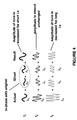
- a photo-detector 220 In the conventional analogue maintenance detector, as for instance shown in Figure 1, a photo-detector 220 generates an electrical signal proportional to the total incident optical power i.e. the sum of the different powers within each channel. Consequently, as indicated in Figure 4, each actual frequency component present on the respective channel will be summed with the ghost tones of the frequency component appearing on the other wavelengths.
- the actual analogue maintenance signal at frequency f 1 on the channel at ⁇ 1 (which has an amplitude proportional to the power of ⁇ 1 ) will be summed with the in-phase ghost signals appearing on the channels at ⁇ 2 and ⁇ 3 , thus resulting in a total frequency tone having a larger amplitude than the actual frequency tone f 1 on the channel at ⁇ 1 .
- the actual analogue maintenance signal f 3 on the channel at ⁇ 3 will be summed with the two out of phase ghost versions of the analogue maintenance signal at frequency f 3 from channels at ⁇ 1 and ⁇ 2 , thus resulting in a decreased amplitude f 3 component.
- analogue maintenance signal at frequency f 2 on channel ⁇ 2 will be summed both with an in-phase and an out of phase ghost tone from respectively the channel at ⁇ 3 and the channel at ⁇ 1 , the amplitude of the signal will be almost unchanged.
- the amplitudes of the frequency components are normally taken to be proportional to the power within the respective channel. It will thus be appreciated that, due to the ghost tones, the amplitude of the frequency components at relatively shorter wavelengths will be over estimated, and the amplitude of the frequency components at longer wavelengths under estimated, with a corresponding inaccuracy in the estimated power per channel.
- the present inventors have appreciated that this is likely to be a problem in optical communication systems utilising signals experiencing SRS, and propose apparatus and methods that allow improved accuracy in measuring such frequency components of analogue maintenance signals.
- Figure 5 shows an apparatus 500 for detecting an analogue maintenance signal in accordance with a preferred embodiment of the present invention.
- the apparatus comprises an input 502 for receiving an optical signal comprising a plurality of channels.
- the optical signal comprises three equally spaced channels at wavelengths ⁇ 1 , ⁇ 2 and ⁇ 3 ( as described in relation to Figures 3 and 4).
- the received optical signal is passed to a splitter 504.
- the splitter acts to split the received optical signal into two bands of wavelength.
- the two bands are roughly of equal blocks of wavelength, with the lower wavelength band being provided via output 506 to Arm 1 (510, 514, 518), and the higher wavelength band being provided via output 508 to Arm 2 (512, 516, 520) of the detector.
- the first band contains the short wavelength channel signals at ⁇ 1 and ⁇ 2
- the second higher band contains ⁇ 3 .
- Each arm of the detector comprises a respective photo-detector 510, 512 arranged to produce an output signal proportional to the total power of the input optical signal.
- each arm incorporates a filter 518, 520 arranged to pass substantially only the frequencies of the analogue maintenance signals within the optical band input to the relevant arm.
- the first arm has the two lower wavelength signals ⁇ 1 , ⁇ 2 , with respective analogue maintenance signals f 1 , f 2 .
- the low pass filter 518 is thus arranged to pass f 1 and f 2 , but not pass f 3 i.e. the analogue maintenance signal of the channel at ⁇ 3 (which is input to Arm 2).
- the high pass filter 520 is arranged to pass f 3 , but not pass the lower frequency analogue maintenance signals f 1 and f 2 .
- each arm further contains an electrical amplifier 514, 516, arranged to amplify the output signal of the respective photo detector 510, 512, prior to input to the filter.
- each filter could subsequently be separately analysed to determine the separate frequency components present, and the amplitudes of the frequency components.
- the preferred embodiment shown in Figure 5 re-combines the two output signals from the filters 518, 520 by an adder 522.
- the output of the adder 522 is provided to a band pass filter, arranged to pass all analogue maintenance frequency signals, and to filter out extremely low and extremely high components that might be present in signal (e.g. due to the information bit-rate).
- This band pass filter 524 is the equivalent filter to the band pass filter 250 shown in Figure 1.
- the output of the band pass filter 524 can subsequently be converted to a digital signal by the analogue to digital converter 526, and then processed by a digital signal processor 528 so as to determine the frequency components present (e.g. using Fast Fourier Transform processing). Subsequently, the frequency components present and the per channel power can be passed to a control unit 530.
- the control unit 530 can use this information to control the performance of at least one of: a node incorporating the detector; a link through which at least a portion of the optical signal has been transmitted, or will be transmitted subsequent to the analogue maintenance signal measurement being made; or overall control of the connectivity within the network.
- Computer software 550 may be used to implement control within the control unit 530, and/or may be used to control the detector 500, and/or perform part of the signal processing within the detector 500 (e.g. Fourier analysis of the electrical signal to determine the frequency components present, and the amplitudes of such frequency components).
- the above apparatus does not function so as to remove all of the ghost tones of the analogue maintenance signals. However, it does serve to remove those ghost tones originating from channels a relatively long wavelength away from the relevant channel. Consequently, the accuracy of the detected amplitude of the relevant analogue maintenance tone is significantly improved.
- the splitter 504 has been described as splitting the received optical signal into two separate bands of wavelengths.
- a splitter could be a coarse Wavelength Division Multiplexer (WDM).
- WDM Wavelength Division Multiplexer
- the splitter could be arranged to split the received optical signal into three or more separate bands of wavelength.
- the analogue maintenance signal on each channel has been referred to as a single frequency or tone.
- analogue maintenance signals might be provided by modulating each channel using a different modulation format, for instance one that would occupy a band of frequencies rather than a single frequency. It will also be appreciated that the present invention is applicable to such modulation formats.
- the splitter acts to split the optical signal into continuous bands of wavelength, for example a first band including all of the lower wavelength channels, and a second band including all of the higher wavelength channels.
- the analogue maintenance frequencies are allocated to the channels such that, once the optical signal has been split into bands, the analogue maintenance signals for any band will fall within a respective, non-overlapping range of frequencies. This facilitates filtering of the frequency signals.
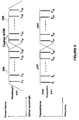
- Figure 6 shows an example where forty channels (at wavelengths ⁇ 1 , ⁇ 2 , ⁇ 3 , .... ⁇ 40 ) are utilised, each having a respective analogue maintenance frequency (f 1 , f 2 , f 3 ...f 40 ).
- Figure 6 illustrates the wavelength plan i.e. output 506 of the WDM filter can be arranged to pass the channels at wavelengths ⁇ 1 - ⁇ 20 , whilst output 508 of the filter can be used to pass the channels at wavelengths ⁇ 21 - ⁇ 40 .
- the low pass filter 518 is arranged to pass analogue maintenance frequencies f 1 -f 20
- the high pass filter 520 to pass frequencies f 21 -f 40 .
- splitter characteristics can be used other than those shown in Figure 6.
- the splitter need not split the received optical signal into two completely separate optical bands.
- the splitter merely needs to operate so as to ensure that each portion of the respective signal from the splitter contains the majority of the desired optical band, and a minority (i.e. less than 50%) of the undesired optical band(s) signal.
- An alternative embodiment of the present invention utilises a fused fibre coupler as the splitter 504. This offers slightly reduced accuracy compared to a detector incorporating a wavelength division multiplexer, but at a reduced cost.
- Fused fibre couplers typically have a sinusoidal transmittance behaviour with respect to wavelength.
- each output 506, 508 of the fused fibre coupler is arranged to have full excursion across the total range of wavelengths within the optical signal.
- a typical band of wavelength utilised to transmit optical signals is the C-band of Erbium, with channels being arranged between wavelengths 1530 and 1560nm.
- Figure 7 illustrates the transmittance response of a fuse fibre coupler acting as a splitter 504 for an optical signal containing only channels within the C-band.
- the first output 506 of the splitter is arranged to have a peak transmittance at the low wavelength end of the signal (1530nm), and a minimum transmittance at the high wavelength end of the band (1560nm), with the other output 508 having a converse transmittance response.
- Figure 8 illustrates the wavelength and frequency plan for a detector incorporating such a fused fibre coupler splitter.
- each of the optical wavelengths has a respective analogue maintenance frequency signal at a similarly increasing frequency. Consequently the low pass filter within Arm 1 connected to output 506 of the coupler is arranged to pass the lower frequency analogue maintenance signals, whilst the high pass filter on the other arm is arranged to pass the higher frequency analogue maintenance signals corresponding to the longer wavelength optical channels.
- the analogue maintenance tones received at the input to the digital signal processor will have different amplitudes even if all of the channels are of equal power and no SRS has taken place.
- the left hand chart in Figure 9 shows the resulting reduction in accuracy due to such coupler and filter characteristics.
- this error is a fixed receiver offset, and can therefore be corrected e.g. by using software, to give the accurate response illustrated in the right hand chart of Figure 9.
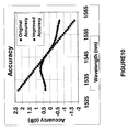
- Figure 10 shows a comparison between the predicted accuracy of a conventional analogue maintenance detector ("original accuracy"), corresponding to performance of a detector has shown in Figure 1, and a detector as shown in Figure 5 ("improved accuracy") at different wavelengths.
- Original accuracy a conventional analogue maintenance detector
- improved accuracy a detector as shown in Figure 5
- This chart assumes that the low pass and high pass filters were fourth order Chebyshev filters, and takes into account the SRS ghost tone generation, the coupler response, the filtering attenuation and the phase.
- the original accuracy varies from approximately 2.3 to -1.8dB across the C-band.
- the present invention increases the accuracy of the measurement of the power per wavelength such that the accuracy always remains within the range 0.6 to -0.6dB.
- Figure 11 provides performance predictions comparing the original and improved analogue maintenance detection techniques for different system configurations.
- the spacing between channels was chosen such that the channels covered the entire C-band.
- the graphs indicate for each number of channels, the maximum number of spans of optical fibre that maintain the analogue maintenance detection accuracy within a predetermined limit (0.5dB and 1dB). It will also been seen that by utilising an analogue maintenance technique in accordance with the present invention, a greater number of lengths of optical fibre can utilised compared with the conventional technique whilst still maintaining a given level of accuracy.
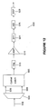
- the analogue maintenance detection apparatus 600 shown in Figure 12 is arranged to receive a tap of an optical signal at input 502.
- Splitter 504 splits the optical signal into two bands of equal blocks of wavelength, with one wavelength band being provided by output 506 to a first input of an optical switch 605, and the other wavelength band being provided via output 508 to a second input of the optical switch.
- the optical switch 605 has two inputs and a single output.
- the switch 605 is arranged to switch one of the inputs to the output, the output being subsequently detected by photo detector 510.
- the photo detector 510 is arranged to produce an output signal proportional to the total power of the total power of the input optical signal. Hence, by toggling the optical switch so as to direct in turn the two bands of wavelength to the photo detector, the photo detector can separately detect both the first band and the second band.
- the resulting optical signal relating to the detected optical band is amplified by electrical amplifier 514, filtered by band pass filter 524 and converted to a digital signal by analogue to digital converter 526.
- the low pass filtering and the high pass filtering are performed digitally by the digital signal processor 628.
- the two bands of optical signal are separately detected by respective photo detectors 510, 512.
- An electrical switch 710 is arranged to switch either the electrical signal from photo diode 510 or the electrical signal from photo diode 512 to the amplifier 514. Hence, by using the switch to take alternate samples from the two photo diodes, and individually processing each of the signals, an improved analogue maintenance detection can be performed. Again, in this instance, the low pass filtering and the high pass filtering (performed by the filters 518, 520 in Figure 5) are performed by the digital signal processor 628.
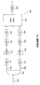
- FIGS 14 and 15 show similar apparatus, in which each of the optical bands from the splitter outputs 506, 508 are separately photo detected, electrically amplified, band pass filtered and analogue to digitally converted.
- a digital switch 827 acts to direct either the digital signal corresponding to the first band to the digital signal processor 628, or the digital signal corresponding to the second band to the digital signal processor 628. Again, by toggling the switch, alternative samples can be taken of each signal.
- the digital signal processor 928 has two inputs.
- the digital signal processor can be arranged to either process each of the inputs in parallel, or alternatively switch between the inputs (so as to effectively combine the operation of digital switch 827 and DSP 628 shown in Figure 14).
- the DSP acts to perform the low pass filtering and the high pass filtering.
- Another aspect provides a method of offering a data transmission service over a network utilising optical signal processing in accordance with the present invention.
Landscapes
- Engineering & Computer Science (AREA)
- Computer Networks & Wireless Communication (AREA)
- Signal Processing (AREA)
- Physics & Mathematics (AREA)
- Electromagnetism (AREA)
- Optical Communication System (AREA)
- Investigating, Analyzing Materials By Fluorescence Or Luminescence (AREA)
Applications Claiming Priority (2)
| Application Number | Priority Date | Filing Date | Title |
|---|---|---|---|
| US254109 | 2002-09-25 | ||
| US10/254,109 US7184672B2 (en) | 2002-09-25 | 2002-09-25 | Analogue maintenance detection |
Publications (1)
| Publication Number | Publication Date |
|---|---|
| EP1404044A2 true EP1404044A2 (de) | 2004-03-31 |
Family
ID=31977814
Family Applications (1)
| Application Number | Title | Priority Date | Filing Date |
|---|---|---|---|
| EP20030078002 Withdrawn EP1404044A2 (de) | 2002-09-25 | 2003-09-22 | Verbesserungen in und in Bezug auf die Detektion von analogen Wartungssignalen |
Country Status (3)
| Country | Link |
|---|---|
| US (1) | US7184672B2 (de) |
| EP (1) | EP1404044A2 (de) |
| CA (1) | CA2442375A1 (de) |
Cited By (2)
| Publication number | Priority date | Publication date | Assignee | Title |
|---|---|---|---|---|
| WO2010002425A1 (en) * | 2008-06-30 | 2010-01-07 | Alcatel-Lucent Usa Inc. | Apparatus and method for improving the tolerance of tone-based optical channel monitoring to stimulated raman scattering |
| EP3078140A4 (de) * | 2013-12-27 | 2016-12-21 | Huawei Tech Co Ltd | System und verfahren zur verringerung von stimuliertem ramanstreuungsübersprechen in der kanalüberwachung |
Families Citing this family (6)
| Publication number | Priority date | Publication date | Assignee | Title |
|---|---|---|---|---|
| CA2571836A1 (en) | 2004-07-15 | 2006-01-19 | Metconnex Canada Inc. | Shared optical performance monitoring |
| US7477852B2 (en) * | 2005-01-31 | 2009-01-13 | Alcatel-Lucent Usa Inc. | Optical receiver apparatus and method |
| US8175113B2 (en) * | 2008-06-30 | 2012-05-08 | Infinera Corporation | Communication network with node bypassed co-routed multi-channel traffic |
| JP6427992B2 (ja) * | 2014-06-30 | 2018-11-28 | 富士通株式会社 | 光伝送システム、送信機、受信機、及び、光伝送方法 |
| US10451446B2 (en) | 2018-01-19 | 2019-10-22 | Rosemount Aerospace Inc. | System for interfacing with an optically-powered sensor |
| CN111385021A (zh) * | 2018-12-29 | 2020-07-07 | 上海嘉慧光电子技术有限公司 | 一种基于载波调制的多波长光功率监测系统及方法 |
Family Cites Families (3)
| Publication number | Priority date | Publication date | Assignee | Title |
|---|---|---|---|---|
| US6212310B1 (en) * | 1996-10-22 | 2001-04-03 | Sdl, Inc. | High power fiber gain media system achieved through power scaling via multiplexing |
| JP3588984B2 (ja) * | 1997-08-20 | 2004-11-17 | Kddi株式会社 | 光パワー計測システム並びにそのための端局及び中継器 |
| US6281995B1 (en) * | 2000-04-11 | 2001-08-28 | Lockheed Martin Corporation | Use of cross tap equalization to reduce crosstalk arising from inadequate optical filtering in a wavelength division multiplexed optical link |
-
2002
- 2002-09-25 US US10/254,109 patent/US7184672B2/en not_active Expired - Lifetime
-
2003
- 2003-09-22 EP EP20030078002 patent/EP1404044A2/de not_active Withdrawn
- 2003-09-24 CA CA002442375A patent/CA2442375A1/en not_active Abandoned
Cited By (3)
| Publication number | Priority date | Publication date | Assignee | Title |
|---|---|---|---|---|
| WO2010002425A1 (en) * | 2008-06-30 | 2010-01-07 | Alcatel-Lucent Usa Inc. | Apparatus and method for improving the tolerance of tone-based optical channel monitoring to stimulated raman scattering |
| US8078054B2 (en) | 2008-06-30 | 2011-12-13 | Alcatel Lucent | Apparatus and method for improving the tolerance of tone-based optical channel monitoring to stimulated Raman scattering |
| EP3078140A4 (de) * | 2013-12-27 | 2016-12-21 | Huawei Tech Co Ltd | System und verfahren zur verringerung von stimuliertem ramanstreuungsübersprechen in der kanalüberwachung |
Also Published As
| Publication number | Publication date |
|---|---|
| US20040057729A1 (en) | 2004-03-25 |
| US7184672B2 (en) | 2007-02-27 |
| CA2442375A1 (en) | 2004-03-25 |
Similar Documents
| Publication | Publication Date | Title |
|---|---|---|
| US8078054B2 (en) | Apparatus and method for improving the tolerance of tone-based optical channel monitoring to stimulated Raman scattering | |
| JP3072047B2 (ja) | 波長多重光伝送装置および光中継器 | |
| JP4776437B2 (ja) | 光通信システムの振幅変調 | |
| US5923453A (en) | Apparatus for measuring optical transmission line property and optical wavelength multiplexing transmission apparatus | |
| US6040933A (en) | Method and apparatus for channel equalization in wavelength division multiplexed systems | |
| US7302178B2 (en) | System and method for measuring power of optical signals carried over a fiber optic link | |
| EP0911994B1 (de) | Überwachung der optischen Signalleistung mit einem Signaturbitmuster in WDM Systemen | |
| WO2013185343A1 (zh) | 抑制导频信号串扰的方法、装置及导频信号接收装置 | |
| US6215583B1 (en) | System with feedback controlled optical amplifiers | |
| US6341024B1 (en) | Channel monitoring apparatus in a wavelength division multiplexing system | |
| US7184672B2 (en) | Analogue maintenance detection | |
| JP2002022612A (ja) | 光特性測定装置、方法、記録媒体 | |
| JP2004515186A (ja) | 性能監視方法、光増幅器、光伝送リンク | |
| JP6497439B2 (ja) | 通信装置、通信方法、及び、通信システム | |
| US20050225844A1 (en) | Optical amplifier apparatus | |
| CN1188969C (zh) | 具有采用偏振调制的光信道监控装置的光网络及其方法 | |
| JP2008245162A (ja) | 波長多重光伝送システム並びに波長多重光伝送方法 | |
| CN117768027A (zh) | 一种光信号调制和监测方法及相关装置 | |
| US6847440B2 (en) | Method for measuring the optical signal-to-noise ratios OSNR in a wavelength division multiplex (WDM) transmission system | |
| JPH1194701A (ja) | 光伝送路監視装置 | |
| JP2002280962A (ja) | コヒーレント光通信システムの光sn検出装置及び方法 | |
| JP2001007766A (ja) | Wdm光インターフェース装置 |
Legal Events
| Date | Code | Title | Description |
|---|---|---|---|
| PUAI | Public reference made under article 153(3) epc to a published international application that has entered the european phase |
Free format text: ORIGINAL CODE: 0009012 |
|
| AK | Designated contracting states |
Kind code of ref document: A2 Designated state(s): AT BE BG CH CY CZ DE DK EE ES FI FR GB GR HU IE IT LI LU MC NL PT RO SE SI SK TR |
|
| AX | Request for extension of the european patent |
Extension state: AL LT LV MK |
|
| STAA | Information on the status of an ep patent application or granted ep patent |
Free format text: STATUS: THE APPLICATION HAS BEEN WITHDRAWN |
|
| 18W | Application withdrawn |
Effective date: 20051011 |