EP1404162B1 - Ballast avec protection adaptative en cas de détection de fin de durée de vie - Google Patents
Ballast avec protection adaptative en cas de détection de fin de durée de vie Download PDFInfo
- Publication number
- EP1404162B1 EP1404162B1 EP03020634A EP03020634A EP1404162B1 EP 1404162 B1 EP1404162 B1 EP 1404162B1 EP 03020634 A EP03020634 A EP 03020634A EP 03020634 A EP03020634 A EP 03020634A EP 1404162 B1 EP1404162 B1 EP 1404162B1
- Authority
- EP
- European Patent Office
- Prior art keywords
- ballast
- inverter
- voltage
- blocking capacitor
- control circuit
- Prior art date
- Legal status (The legal status is an assumption and is not a legal conclusion. Google has not performed a legal analysis and makes no representation as to the accuracy of the status listed.)
- Expired - Lifetime
Links
- 230000000903 blocking effect Effects 0.000 claims abstract description 29
- 239000003990 capacitor Substances 0.000 claims abstract description 29
- 230000001681 protective effect Effects 0.000 claims description 5
- 230000004044 response Effects 0.000 claims description 4
- 238000012544 monitoring process Methods 0.000 claims 3
- 238000001514 detection method Methods 0.000 description 9
- 230000003044 adaptive effect Effects 0.000 description 2
- 238000013459 approach Methods 0.000 description 2
- 206010011906 Death Diseases 0.000 description 1
- 230000008901 benefit Effects 0.000 description 1
- 230000001419 dependent effect Effects 0.000 description 1
- 238000004519 manufacturing process Methods 0.000 description 1
- 238000005259 measurement Methods 0.000 description 1
- 238000000034 method Methods 0.000 description 1
- 238000012986 modification Methods 0.000 description 1
- 230000004048 modification Effects 0.000 description 1
- 238000013021 overheating Methods 0.000 description 1
- 230000008569 process Effects 0.000 description 1
- 238000012360 testing method Methods 0.000 description 1
Images


Classifications
-
- H—ELECTRICITY
- H05—ELECTRIC TECHNIQUES NOT OTHERWISE PROVIDED FOR
- H05B—ELECTRIC HEATING; ELECTRIC LIGHT SOURCES NOT OTHERWISE PROVIDED FOR; CIRCUIT ARRANGEMENTS FOR ELECTRIC LIGHT SOURCES, IN GENERAL
- H05B41/00—Circuit arrangements or apparatus for igniting or operating discharge lamps
- H05B41/14—Circuit arrangements
- H05B41/26—Circuit arrangements in which the lamp is fed by power derived from DC by means of a converter, e.g. by high-voltage DC
- H05B41/28—Circuit arrangements in which the lamp is fed by power derived from DC by means of a converter, e.g. by high-voltage DC using static converters
- H05B41/282—Circuit arrangements in which the lamp is fed by power derived from DC by means of a converter, e.g. by high-voltage DC using static converters with semiconductor devices
- H05B41/285—Arrangements for protecting lamps or circuits against abnormal operating conditions
- H05B41/2851—Arrangements for protecting lamps or circuits against abnormal operating conditions for protecting the circuit against abnormal operating conditions
- H05B41/2855—Arrangements for protecting lamps or circuits against abnormal operating conditions for protecting the circuit against abnormal operating conditions against abnormal lamp operating conditions
Definitions
- the present invention relates to the general subject of circuits for powering discharge lamps. More particularly, the present invention relates to a ballast with adaptive end-of-lamp-life protection.
- V BLOCK direct current blocking capacitor
- V DC DC rail voltage
- a number of existing end-of-lamp-life protection circuits monitor V BLOCK as a reliable indicator of imminent lamp failure. A number of these circuits consider a lamp to be in a failure mode when V BLOCK departs from its normal value by more than a predetermined threshold amount. Such a protection circuit is known from US 5 808 422 .
- the predetermined threshold amount be suitably small in relation to the normal value of V BLOCK .
- a typical protection circuit will consider the lamp to be in the failure mode if V BLOCK departs from its normal value of 225 volts by as little as 10 volts (i.e., 4%) in either direction; that is, the lamp is considered to be in the failure mode if V BLOCK either exceeds 235 volts or falls below 215 volts.
- these minimum (i.e., 215 volts) and maximum (i.e., 235 volts) values are "designed in"; that is, they are specified on an a priori basis, regardless of the actual value of V BLOCK during normal operation.
- V BLOCK is generally monitored via a resistive voltage-divider network that is coupled in parallel with the DC blocking capacitor.
- the tolerances of the voltage-divider resistors are a first source of possible error.
- the protection circuit itself generally includes a digital control circuit or microcontroller in which the supply voltage (V CC ) can vary by as much as 5%. This introduces another possible source of detection error. Additionally, small differences in the dead-time and/or duty cycle at which the inverter switches are driven will cause V BLOCK to differ at least somewhat from its ideal normal value of V DC /2.
- V DC itself has an associated tolerance (e.g., typically on the order of about 2% or so).
- each of the aforementioned sources of possible error is temperature-dependent to some extent, and may thus be aggravated by the often considerable changes in temperature that occur during operation of the ballast.
- the band of detection In order to avoid the detection problems arising from component tolerances, one would have to set a band of detection that is considerably less tight than in the above example. For instance, the band of detection would have to be increased to ⁇ 20 volts (rather than ⁇ 10 volts). Unfortunately, such "opening up" of the band of detection degrades the quality of protection afforded by the protection circuit, and may not even be an option for ballasts that operate certain types of lamps.
- ballast with an end-of-lamp-life protection circuit that is capable of providing a tight band of detection and that is relatively insensitive to component tolerances and other sources of detection error.
- Such a ballast would represent a considerable advance over the prior art.
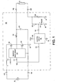
- Ballast 100 for powering at least one gas discharge lamp 10 is described in FIG. 1 .
- Ballast 100 comprises a pair of input connections 102,104, first and second output connection 106,108, an inverter 110,120,122 with a series-resonant output circuit 124,126, a direct current (DC) blocking capacitor 130, and a control circuit 140.
- DC direct current
- Input connections 102,104 are adapted to receive a source of alternating current, such as 277 volts (rms) at 60 hertz.
- Output connections 106,108 are adapted for connection to gas discharge lamp 10.
- Direct current (DC) blocking capacitor 130 is coupled between second output connection 108 and circuit ground 30.
- Inverter 110,120,122 is operably coupled between input connections 102,104 and first output connection 106, and includes an inverter drive circuit 110 for providing switching of inverter transistors 120,122 at a predetermined operating frequency.
- Inverter drive circuit 110 has a supply input 114 for receiving operating power (+V CC ), and a protection input 112.
- inverter drive circuit 110 takes protective action (e.g., terminating inverter switching or operating the inverter at a frequency that is substantially higher than the predetermined operating frequency) so as to prevent any damage to the inverter and the lamp sockets.
- Control circuit 140 has a supply input 146 for receiving operating power (+VCC), a control input 142 that is operably coupled to DC blocking capacitor 130, and a control output 144 that is coupled to the protection input 112 of inverter drive circuit 110.
- Control circuit 140 is preferably implemented via a suitable programmable microcontroller that is programmed to operate in the following manner. Following initial application of power to ballast 100, control circuit 140 measures the voltage across DC blocking capacitor 130 and stores that voltage as a reference value. Following each subsequent application of power to ballast 100, control circuit 140 monitors the voltage across DC blocking capacitor 130. If the measured voltage across DC blocking capacitor 130 departs from the stored reference value by more than a predetermined threshold amount (e.g., 10 volts), control circuit 140 provides the fault signal at control output 144 (and, therefore, at protection input 112).
- a predetermined threshold amount e.g. 10 volts
- ballast 100 further includes a resistive voltage-divider network comprising a first resistor 132 and a second resistor 134.
- First resistor 132 is coupled between second output connection 108 and control input 142 of control circuit 140.
- Second resistor 134 is coupled between control input 142 and circuit ground 30.
- the voltage across second resistor 134 (e.g., 2.25 volts or so under normal operation) is a scaled down version of the voltage across DC blocking capacitor 130.
- the voltage V SENSE across second resistor 134 is monitored and measured in lieu of the actual voltage across DC blocking capacitor 130.
- the predetermined threshold amount is scaled down by the same factor (i.e., 0.1 volts instead of 10 volts).
- resistors 132,134 can be selected such that the corresponding voltage V SENSE across resistor 134 is 2.25 volts.
- V THRESH should be set at 0.1 volts.
- the reference value is measured and stored with a resistive load (e.g., 800 ohms) coupled between output connections 106,108.
- a resistive load e.g. 800 ohms
- ballast 100 and control circuit 140 provide an adaptive scheme that allows for a tight band of fault detection that is devoid of any errors due to component tolerances.
- ballast 100 and control circuit 140 Flowcharts that describe the preferred operation of ballast 100 and control circuit 140 are given in FIGs. 2 and 3 .
- FIG. 2 describes a preferred routine 200 by which the reference value V REF of the voltage across DC blocking capacitor 130 is measured and stored.
- the ballast output is connected to a resistive load.
- AC power is applied to the ballast.
- the voltage V SENSE across the lower divider resistor i.e., resistor 134 in FIG. 1
- the reference voltage V REF is set equal to the measured value of V SENSE , and stored accordingly.
- FIG. 3 describes a preferred routine 300 by which the voltage across DC blocking capacitor 130 is monitored for an end-of-lamp-life condition.
- the ballast output is connected to a lamp load.
- AC power is applied to the ballast.
- the voltage V SENSE across the lower divider resistor i.e., resistor 134 in FIG. 1
- the measured value of V SENSE is compared with V REF and the predetermined threshold voltage V THRESH ⁇ As long as V SENSE is within the limits assigned for normal operation, no protective action will be taken and V SENSE will continue to be monitored.
- V SENSE either exceeds V REF + V THRESH or falls below V REF - V THRESH .
- appropriate protective action that consists of either shutting down the inverter or shifting the inverter to a low power mode (i.e., operating the inverter at a frequency that is substantially higher than the normal operating frequency) will be taken at step 312.
Landscapes
- Circuit Arrangements For Discharge Lamps (AREA)
- Inverter Devices (AREA)
- Power Conversion In General (AREA)
Claims (12)
- Ballast ( 100 ) pour alimenter au moins une lampe 10) à décharge dans un gaz comprenant :une paire de connexions ( 102, 104 ) d'entrée conçue pour recevoir une source de courant ( 20 ) alternatif ;des première et deuxième connexions ( 106, 108 ) de sortie conçues pour une connexion à la lampe ( 10 ) à décharge dans un gaz ;un onduleur ( 120, 122 ) couplé fonctionnellement entre les connexions ( 102, 104 ) d'entrée et la première connexion ( 106 ) de sortie, l'onduleur comprenant un circuit d'attaque d'onduleur pour procurer une commutation de l'onduleur à une fréquence de fonctionnement déterminée à l'avance, le circuit d'attaque de l'onduleur ayant une entrée ( 112 ) de protection et pouvant fonctionner en réaction à l'application d'un signal de défaut à l'entrée de protection pour effectuer une action de protection ( figure 3 ) ;un condensateur ( 130 ) de blocage de courant continu ( DC ) monté entre la deuxième connexion de sortie et la terre 30 ) du circuit ;un circuit ( 140 ) de commande ayant une entrée 142 ) de commande couplée fonctionnellement au condensateur de blocage du courant continu et une sortie ( 144 ) de commande couplée à entrée de protection du circuit d'attaque de l'onduleur, caractérisé en ce que le circuit ( 140 ) de commande peut fonctionner :(i) à la suite de l'application initiale de courant au ballast pour mesurer la tension aux bornes du condensateur de blocage du courant continu et pour stocker cette tension comme valeur de référence ( figure 2 ) ; et(ii) à la suite de chaque application subséquente de courant au ballast :a) pour contrôler la tension aux bornes du condensateur de blocage du courant continu ; etb) en réaction à la tension aux bornes du condensateur de blocage du courant continu, s'écartant de la valeur de référence de plus qu'une quantité de seuil déterminée à l'avance, fournir le signal de défaut à la sortie de commande ( figure 3 ).
- Ballast suivant la revendication 1 comprenant, en outre :une première résistance ( 132 ) montée entre la deuxième connexion ( 108 ) de sortie et l'entrée ( 142 ) de commande du circuit de commande ; etune deuxième résistance ( 134 ) montée entre l'entrée de commande du circuit de commande et la terre du circuit.
- Ballast suivant la revendication 2, dans lequel la tension aux bornes de la deuxième résistance ( 134 ) est contrôlée et mesurée au lieu de la tension aux bornes du condensateur ( 130 ) de blocage du courant continu.
- Ballast suivant la revendication 1, dans lequel la quantité de seuil déterminée à l'avance est de l'ordre d'environ 10 volts.
- Ballast suivant la revendication 1, dans lequel la valeur de référence est mesurée par une charge résistive montée entre la première et la deuxième connexion de sortie.
- Ballast suivant la revendication 1, dans lequel le circuit d'attaque de l'onduleur peut fonctionner pour effectuer une action de protection qui comprend l'un de :mettre fin à la commutation de l'onduleur ; etfaire fonctionner l'onduleur à une fréquence qui est sensiblement plus haute que la fréquence de fonctionnement déterminée à l'avance ( figure 3 ).
- Circuit ( 40 ) de commande pour fournir une protection de fin de vie de lampe dans un ballast ( 100 ) électronique, ayant un onduleur ( 120, 122 ) et un condensateur (130) de blocage du courant continu ( DC ) monté en série avec une sortie du ballast, caractérisé en ce que le circuit de protection peut fonctionner pour exécuter les stades suivantes :(i) mesure d'une valeur de référence pour la tension aux bornes du condensateur ( 130 ) de blocage du courant continu ;(ii) mémorisation de la valeur de référence ( figure 2 ) ;(iii) contrôle de la tension aux bornes du condensateur ( 130 ) de blocage du courant continu ; et(iv) protection de l'onduleur et des culots de la lampe en réaction au fait que la tension aux bornes du condensateur de blocage du courant continu s'écarte la valeur de référence de plus qu'une quantité de seuil déterminée à l'avance ( figure 3 ).
- Circuit de commande suivant la revendication 7, dans lequel on effectue le stade de mesure après un premier laps de temps suivant une application initiale de courant au ballast ( figure 2 ).
- Circuit de commande suivant la revendication 7, dans lequel on effectue les stades de mesure et de mémorisation avec une charge résistive couplée à la sortie du ballast.
- Circuit de commande suivant la revendication 7, dans lequel on effectue le stade de contrôle après un deuxième laps de temps suivant des applications subséquences de courant au ballast.
- Circuit de commande suivant la revendication 7, dans lequel on effectue les stades de contrôle et de protection avec une charge de lampe couplée à la sortie du ballast.
- Circuit de commande suivant la revendication 7, dans lequel le stade de protection comprend l'un de :neutralisation de l'onduleur ; etfonctionnement de l'onduleur à une fréquence qui est sensiblement plus haute que la fréquence de fonctionnement normale de l'onduleur ( figure 3 ).
Applications Claiming Priority (2)
| Application Number | Priority Date | Filing Date | Title |
|---|---|---|---|
| US10/261,011 US6741043B2 (en) | 2002-09-30 | 2002-09-30 | Ballast with adaptive end-of-lamp-life protection |
| US261011 | 2002-09-30 |
Publications (3)
| Publication Number | Publication Date |
|---|---|
| EP1404162A2 EP1404162A2 (fr) | 2004-03-31 |
| EP1404162A3 EP1404162A3 (fr) | 2008-03-12 |
| EP1404162B1 true EP1404162B1 (fr) | 2009-07-01 |
Family
ID=31977935
Family Applications (1)
| Application Number | Title | Priority Date | Filing Date |
|---|---|---|---|
| EP03020634A Expired - Lifetime EP1404162B1 (fr) | 2002-09-30 | 2003-09-10 | Ballast avec protection adaptative en cas de détection de fin de durée de vie |
Country Status (5)
| Country | Link |
|---|---|
| US (1) | US6741043B2 (fr) |
| EP (1) | EP1404162B1 (fr) |
| AT (1) | ATE435586T1 (fr) |
| CA (1) | CA2429785C (fr) |
| DE (1) | DE60328151D1 (fr) |
Families Citing this family (9)
| Publication number | Priority date | Publication date | Assignee | Title |
|---|---|---|---|---|
| DE102005017324A1 (de) | 2005-04-14 | 2006-10-19 | Patent-Treuhand-Gesellschaft für elektrische Glühlampen mbH | Elektronisches Vorschaltgerät für eine Lampe |
| WO2008070138A2 (fr) * | 2006-12-05 | 2008-06-12 | Rambus Inc. | Procédés et circuits pour une distribution asymétrique d'égalisation de canaux entre des dispositifs |
| US7327101B1 (en) | 2006-12-27 | 2008-02-05 | General Electric Company | Single point sensing for end of lamp life, anti-arcing, and no-load protection for electronic ballast |
| US7843141B1 (en) | 2007-11-19 | 2010-11-30 | Universal Lighting Technologies, Inc. | Low cost step dimming interface for an electronic ballast |
| US8482213B1 (en) | 2009-06-29 | 2013-07-09 | Panasonic Corporation | Electronic ballast with pulse detection circuit for lamp end of life and output short protection |
| CN101938880B (zh) * | 2009-06-30 | 2014-09-10 | 通用电气公司 | 用于一个或多个灯的具有寿命终止保护的镇流器 |
| US8384310B2 (en) | 2010-10-08 | 2013-02-26 | General Electric Company | End-of-life circuit for fluorescent lamp ballasts |
| US8564216B1 (en) * | 2011-02-02 | 2013-10-22 | Universal Lighting Technologies, Inc. | Asymmetric end-of-life protection circuit for fluorescent lamp ballasts |
| US8947020B1 (en) | 2011-11-17 | 2015-02-03 | Universal Lighting Technologies, Inc. | End of life control for parallel lamp ballast |
Family Cites Families (5)
| Publication number | Priority date | Publication date | Assignee | Title |
|---|---|---|---|---|
| US5475284A (en) * | 1994-05-03 | 1995-12-12 | Osram Sylvania Inc. | Ballast containing circuit for measuring increase in DC voltage component |
| US5808422A (en) * | 1996-05-10 | 1998-09-15 | Philips Electronics North America | Lamp ballast with lamp rectification detection circuitry |
| US5869935A (en) * | 1997-05-07 | 1999-02-09 | Motorola Inc. | Electronic ballast with inverter protection circuit |
| US6366032B1 (en) * | 2000-01-28 | 2002-04-02 | Robertson Worldwide, Inc. | Fluorescent lamp ballast with integrated circuit |
| US6362575B1 (en) * | 2000-11-16 | 2002-03-26 | Philips Electronics North America Corporation | Voltage regulated electronic ballast for multiple discharge lamps |
-
2002
- 2002-09-30 US US10/261,011 patent/US6741043B2/en not_active Expired - Fee Related
-
2003
- 2003-05-23 CA CA2429785A patent/CA2429785C/fr not_active Expired - Fee Related
- 2003-09-10 AT AT03020634T patent/ATE435586T1/de not_active IP Right Cessation
- 2003-09-10 DE DE60328151T patent/DE60328151D1/de not_active Expired - Lifetime
- 2003-09-10 EP EP03020634A patent/EP1404162B1/fr not_active Expired - Lifetime
Also Published As
| Publication number | Publication date |
|---|---|
| CA2429785C (fr) | 2011-09-27 |
| CA2429785A1 (fr) | 2004-03-30 |
| EP1404162A3 (fr) | 2008-03-12 |
| DE60328151D1 (de) | 2009-08-13 |
| EP1404162A2 (fr) | 2004-03-31 |
| ATE435586T1 (de) | 2009-07-15 |
| US6741043B2 (en) | 2004-05-25 |
| US20040061455A1 (en) | 2004-04-01 |
Similar Documents
| Publication | Publication Date | Title |
|---|---|---|
| CN100392546C (zh) | 具有功率因数校正的单片镇流器控制 | |
| US5883473A (en) | Electronic Ballast with inverter protection circuit | |
| CA2148399C (fr) | Circuit de protection pour lampe a decharge | |
| US5828177A (en) | Light circuit for discharge lamp | |
| FI94918C (fi) | Esikytkentälaite purkauslamppua varten | |
| KR101390424B1 (ko) | 주파수-진단 램프 결함 보호 회로를 가진 안정기 | |
| JP5777114B2 (ja) | ランプ用電子バラスト回路 | |
| US7528558B2 (en) | Ballast with ignition voltage control | |
| US6650514B2 (en) | Protection circuit for a fluorescent lamp | |
| US6545432B2 (en) | Ballast with fast-responding lamp-out detection circuit | |
| US6741043B2 (en) | Ballast with adaptive end-of-lamp-life protection | |
| US8193727B2 (en) | Lamp end of life protection circuit and method for an electronic dimming ballast | |
| US6281641B1 (en) | Electronic ballast for one or more lamps | |
| US8203282B2 (en) | Electronic ballast with lamp end of life detection and protection circuits | |
| CA2429430C (fr) | Ballast a circuit de protection contre les defauts de mise a la terre de la lampe | |
| CN1210997C (zh) | 给荧光灯供电的装置 | |
| US8729817B2 (en) | Latching circuit for ballast | |
| JP3832053B2 (ja) | 放電灯点灯装置 | |
| KR100946152B1 (ko) | Lcd 백라이트 인버터 | |
| CA2311891A1 (fr) | Methode d'exploitation d'au moins une lampe fluorescente et d'un ballast electronique connexe | |
| EP0776148B1 (fr) | Circuit de sécurité pour le régulateur de puissance de tubes fluorescents | |
| US8754582B2 (en) | Detector circuit and method for actuating a fluorescent lamp | |
| JP2617460B2 (ja) | 放電灯点灯装置 | |
| JPH08124683A (ja) | 放電灯の寿命検出制御装置 | |
| JPH0878169A (ja) | 放電灯点灯装置 |
Legal Events
| Date | Code | Title | Description |
|---|---|---|---|
| PUAI | Public reference made under article 153(3) epc to a published international application that has entered the european phase |
Free format text: ORIGINAL CODE: 0009012 |
|
| AK | Designated contracting states |
Kind code of ref document: A2 Designated state(s): AT BE BG CH CY CZ DE DK EE ES FI FR GB GR HU IE IT LI LU MC NL PT RO SE SI SK TR |
|
| AX | Request for extension of the european patent |
Extension state: AL LT LV MK |
|
| PUAL | Search report despatched |
Free format text: ORIGINAL CODE: 0009013 |
|
| AK | Designated contracting states |
Kind code of ref document: A3 Designated state(s): AT BE BG CH CY CZ DE DK EE ES FI FR GB GR HU IE IT LI LU MC NL PT RO SE SI SK TR |
|
| AX | Request for extension of the european patent |
Extension state: AL LT LV MK |
|
| 17P | Request for examination filed |
Effective date: 20080821 |
|
| AKX | Designation fees paid |
Designated state(s): AT BE BG CH CY CZ DE DK EE ES FI FR GB GR HU IE IT LI LU MC NL PT RO SE SI SK TR |
|
| GRAP | Despatch of communication of intention to grant a patent |
Free format text: ORIGINAL CODE: EPIDOSNIGR1 |
|
| GRAS | Grant fee paid |
Free format text: ORIGINAL CODE: EPIDOSNIGR3 |
|
| GRAA | (expected) grant |
Free format text: ORIGINAL CODE: 0009210 |
|
| AK | Designated contracting states |
Kind code of ref document: B1 Designated state(s): AT BE BG CH CY CZ DE DK EE ES FI FR GB GR HU IE IT LI LU MC NL PT RO SE SI SK TR |
|
| REG | Reference to a national code |
Ref country code: GB Ref legal event code: FG4D |
|
| REG | Reference to a national code |
Ref country code: CH Ref legal event code: EP |
|
| REG | Reference to a national code |
Ref country code: IE Ref legal event code: FG4D |
|
| REF | Corresponds to: |
Ref document number: 60328151 Country of ref document: DE Date of ref document: 20090813 Kind code of ref document: P |
|
| PG25 | Lapsed in a contracting state [announced via postgrant information from national office to epo] |
Ref country code: SI Free format text: LAPSE BECAUSE OF FAILURE TO SUBMIT A TRANSLATION OF THE DESCRIPTION OR TO PAY THE FEE WITHIN THE PRESCRIBED TIME-LIMIT Effective date: 20090701 |
|
| NLV1 | Nl: lapsed or annulled due to failure to fulfill the requirements of art. 29p and 29m of the patents act | ||
| PG25 | Lapsed in a contracting state [announced via postgrant information from national office to epo] |
Ref country code: FI Free format text: LAPSE BECAUSE OF FAILURE TO SUBMIT A TRANSLATION OF THE DESCRIPTION OR TO PAY THE FEE WITHIN THE PRESCRIBED TIME-LIMIT Effective date: 20090701 Ref country code: ES Free format text: LAPSE BECAUSE OF FAILURE TO SUBMIT A TRANSLATION OF THE DESCRIPTION OR TO PAY THE FEE WITHIN THE PRESCRIBED TIME-LIMIT Effective date: 20091012 Ref country code: AT Free format text: LAPSE BECAUSE OF FAILURE TO SUBMIT A TRANSLATION OF THE DESCRIPTION OR TO PAY THE FEE WITHIN THE PRESCRIBED TIME-LIMIT Effective date: 20090701 Ref country code: SE Free format text: LAPSE BECAUSE OF FAILURE TO SUBMIT A TRANSLATION OF THE DESCRIPTION OR TO PAY THE FEE WITHIN THE PRESCRIBED TIME-LIMIT Effective date: 20090701 Ref country code: EE Free format text: LAPSE BECAUSE OF FAILURE TO SUBMIT A TRANSLATION OF THE DESCRIPTION OR TO PAY THE FEE WITHIN THE PRESCRIBED TIME-LIMIT Effective date: 20090701 |
|
| PG25 | Lapsed in a contracting state [announced via postgrant information from national office to epo] |
Ref country code: NL Free format text: LAPSE BECAUSE OF FAILURE TO SUBMIT A TRANSLATION OF THE DESCRIPTION OR TO PAY THE FEE WITHIN THE PRESCRIBED TIME-LIMIT Effective date: 20090701 |
|
| PG25 | Lapsed in a contracting state [announced via postgrant information from national office to epo] |
Ref country code: PT Free format text: LAPSE BECAUSE OF FAILURE TO SUBMIT A TRANSLATION OF THE DESCRIPTION OR TO PAY THE FEE WITHIN THE PRESCRIBED TIME-LIMIT Effective date: 20091102 Ref country code: BG Free format text: LAPSE BECAUSE OF FAILURE TO SUBMIT A TRANSLATION OF THE DESCRIPTION OR TO PAY THE FEE WITHIN THE PRESCRIBED TIME-LIMIT Effective date: 20091001 |
|
| PG25 | Lapsed in a contracting state [announced via postgrant information from national office to epo] |
Ref country code: DK Free format text: LAPSE BECAUSE OF FAILURE TO SUBMIT A TRANSLATION OF THE DESCRIPTION OR TO PAY THE FEE WITHIN THE PRESCRIBED TIME-LIMIT Effective date: 20090701 Ref country code: CZ Free format text: LAPSE BECAUSE OF FAILURE TO SUBMIT A TRANSLATION OF THE DESCRIPTION OR TO PAY THE FEE WITHIN THE PRESCRIBED TIME-LIMIT Effective date: 20090701 Ref country code: RO Free format text: LAPSE BECAUSE OF FAILURE TO SUBMIT A TRANSLATION OF THE DESCRIPTION OR TO PAY THE FEE WITHIN THE PRESCRIBED TIME-LIMIT Effective date: 20090701 Ref country code: MC Free format text: LAPSE BECAUSE OF NON-PAYMENT OF DUE FEES Effective date: 20090930 |
|
| REG | Reference to a national code |
Ref country code: CH Ref legal event code: PL |
|
| PLBE | No opposition filed within time limit |
Free format text: ORIGINAL CODE: 0009261 |
|
| STAA | Information on the status of an ep patent application or granted ep patent |
Free format text: STATUS: NO OPPOSITION FILED WITHIN TIME LIMIT |
|
| PG25 | Lapsed in a contracting state [announced via postgrant information from national office to epo] |
Ref country code: BE Free format text: LAPSE BECAUSE OF FAILURE TO SUBMIT A TRANSLATION OF THE DESCRIPTION OR TO PAY THE FEE WITHIN THE PRESCRIBED TIME-LIMIT Effective date: 20090701 Ref country code: SK Free format text: LAPSE BECAUSE OF FAILURE TO SUBMIT A TRANSLATION OF THE DESCRIPTION OR TO PAY THE FEE WITHIN THE PRESCRIBED TIME-LIMIT Effective date: 20090701 |
|
| 26N | No opposition filed |
Effective date: 20100406 |
|
| PG25 | Lapsed in a contracting state [announced via postgrant information from national office to epo] |
Ref country code: IE Free format text: LAPSE BECAUSE OF NON-PAYMENT OF DUE FEES Effective date: 20090910 |
|
| PG25 | Lapsed in a contracting state [announced via postgrant information from national office to epo] |
Ref country code: CH Free format text: LAPSE BECAUSE OF NON-PAYMENT OF DUE FEES Effective date: 20090930 Ref country code: LI Free format text: LAPSE BECAUSE OF NON-PAYMENT OF DUE FEES Effective date: 20090930 Ref country code: GR Free format text: LAPSE BECAUSE OF FAILURE TO SUBMIT A TRANSLATION OF THE DESCRIPTION OR TO PAY THE FEE WITHIN THE PRESCRIBED TIME-LIMIT Effective date: 20091002 |
|
| PG25 | Lapsed in a contracting state [announced via postgrant information from national office to epo] |
Ref country code: IT Free format text: LAPSE BECAUSE OF FAILURE TO SUBMIT A TRANSLATION OF THE DESCRIPTION OR TO PAY THE FEE WITHIN THE PRESCRIBED TIME-LIMIT Effective date: 20090701 |
|
| PG25 | Lapsed in a contracting state [announced via postgrant information from national office to epo] |
Ref country code: LU Free format text: LAPSE BECAUSE OF NON-PAYMENT OF DUE FEES Effective date: 20090910 |
|
| PG25 | Lapsed in a contracting state [announced via postgrant information from national office to epo] |
Ref country code: HU Free format text: LAPSE BECAUSE OF FAILURE TO SUBMIT A TRANSLATION OF THE DESCRIPTION OR TO PAY THE FEE WITHIN THE PRESCRIBED TIME-LIMIT Effective date: 20100102 |
|
| PG25 | Lapsed in a contracting state [announced via postgrant information from national office to epo] |
Ref country code: TR Free format text: LAPSE BECAUSE OF FAILURE TO SUBMIT A TRANSLATION OF THE DESCRIPTION OR TO PAY THE FEE WITHIN THE PRESCRIBED TIME-LIMIT Effective date: 20090701 |
|
| PG25 | Lapsed in a contracting state [announced via postgrant information from national office to epo] |
Ref country code: CY Free format text: LAPSE BECAUSE OF FAILURE TO SUBMIT A TRANSLATION OF THE DESCRIPTION OR TO PAY THE FEE WITHIN THE PRESCRIBED TIME-LIMIT Effective date: 20090701 |
|
| PGFP | Annual fee paid to national office [announced via postgrant information from national office to epo] |
Ref country code: FR Payment date: 20111005 Year of fee payment: 9 Ref country code: GB Payment date: 20110915 Year of fee payment: 9 |
|
| GBPC | Gb: european patent ceased through non-payment of renewal fee |
Effective date: 20120910 |
|
| REG | Reference to a national code |
Ref country code: FR Ref legal event code: ST Effective date: 20130531 |
|
| PG25 | Lapsed in a contracting state [announced via postgrant information from national office to epo] |
Ref country code: GB Free format text: LAPSE BECAUSE OF NON-PAYMENT OF DUE FEES Effective date: 20120910 |
|
| PG25 | Lapsed in a contracting state [announced via postgrant information from national office to epo] |
Ref country code: FR Free format text: LAPSE BECAUSE OF NON-PAYMENT OF DUE FEES Effective date: 20121001 |
|
| PGFP | Annual fee paid to national office [announced via postgrant information from national office to epo] |
Ref country code: DE Payment date: 20140922 Year of fee payment: 12 |
|
| REG | Reference to a national code |
Ref country code: DE Ref legal event code: R119 Ref document number: 60328151 Country of ref document: DE |
|
| PG25 | Lapsed in a contracting state [announced via postgrant information from national office to epo] |
Ref country code: DE Free format text: LAPSE BECAUSE OF NON-PAYMENT OF DUE FEES Effective date: 20160401 |