EP1406288A2 - Plasma Anzeigetafel - Google Patents
Plasma Anzeigetafel Download PDFInfo
- Publication number
- EP1406288A2 EP1406288A2 EP03022274A EP03022274A EP1406288A2 EP 1406288 A2 EP1406288 A2 EP 1406288A2 EP 03022274 A EP03022274 A EP 03022274A EP 03022274 A EP03022274 A EP 03022274A EP 1406288 A2 EP1406288 A2 EP 1406288A2
- Authority
- EP
- European Patent Office
- Prior art keywords
- light
- column direction
- interstice
- display panel
- plasma display
- Prior art date
- Legal status (The legal status is an assumption and is not a legal conclusion. Google has not performed a legal analysis and makes no representation as to the accuracy of the status listed.)
- Withdrawn
Links
Images


Classifications
-
- H—ELECTRICITY
- H01—ELECTRIC ELEMENTS
- H01J—ELECTRIC DISCHARGE TUBES OR DISCHARGE LAMPS
- H01J11/00—Gas-filled discharge tubes with alternating current induction of the discharge, e.g. alternating current plasma display panels [AC-PDP]; Gas-filled discharge tubes without any main electrode inside the vessel; Gas-filled discharge tubes with at least one main electrode outside the vessel
- H01J11/20—Constructional details
- H01J11/34—Vessels, containers or parts thereof, e.g. substrates
- H01J11/36—Spacers, barriers, ribs, partitions or the like
-
- H—ELECTRICITY
- H01—ELECTRIC ELEMENTS
- H01J—ELECTRIC DISCHARGE TUBES OR DISCHARGE LAMPS
- H01J11/00—Gas-filled discharge tubes with alternating current induction of the discharge, e.g. alternating current plasma display panels [AC-PDP]; Gas-filled discharge tubes without any main electrode inside the vessel; Gas-filled discharge tubes with at least one main electrode outside the vessel
- H01J11/10—AC-PDPs with at least one main electrode being out of contact with the plasma
- H01J11/12—AC-PDPs with at least one main electrode being out of contact with the plasma with main electrodes provided on both sides of the discharge space
-
- H—ELECTRICITY
- H01—ELECTRIC ELEMENTS
- H01J—ELECTRIC DISCHARGE TUBES OR DISCHARGE LAMPS
- H01J11/00—Gas-filled discharge tubes with alternating current induction of the discharge, e.g. alternating current plasma display panels [AC-PDP]; Gas-filled discharge tubes without any main electrode inside the vessel; Gas-filled discharge tubes with at least one main electrode outside the vessel
- H01J11/20—Constructional details
- H01J11/34—Vessels, containers or parts thereof, e.g. substrates
- H01J11/44—Optical arrangements or shielding arrangements, e.g. filters, black matrices, light reflecting means or electromagnetic shielding means
-
- H—ELECTRICITY
- H01—ELECTRIC ELEMENTS
- H01J—ELECTRIC DISCHARGE TUBES OR DISCHARGE LAMPS
- H01J2211/00—Plasma display panels with alternate current induction of the discharge, e.g. AC-PDPs
- H01J2211/20—Constructional details
- H01J2211/34—Vessels, containers or parts thereof, e.g. substrates
- H01J2211/44—Optical arrangements or shielding arrangements, e.g. filters or lenses
- H01J2211/444—Means for improving contrast or colour purity, e.g. black matrix or light shielding means
Definitions
- This invention relates to a cell structure for plasma display panels.
- PDP plasma display panels
- Fig. 1 to Fig. 3 illustrate the cell structure of a conventional PDP.
- Fig. 1 is a schematic plan view illustrating the cell structure of the conventional PDP.
- Fig. 2 is a sectional view taken along the VA-VA line in Fig. 1.
- Fig. 3 is a sectional view taken along the VB-VB line.
- the conventional PDP has a front glass substrate 1 serving as the display screen and having a back surface on which a plurality of row electrode pairs (X, Y) each forming a display line L are arranged in parallel and extend in the row direction (the right-left direction in Fig. 1) of the front glass substrate 1.
- Each of the row electrodes X and Y is constituted of transparent electrodes Xa (Ya) each formed of a T-shaped transparent conductive film made of ITO or the like, and a metal-film-made bus electrode Xb (Yb) extending in the row direction of the front glass substrate 1 and connected to the narrow proximal ends (i.e. the foot of the T shape) of the transparent electrodes Xa (Ya).
- the row electrodes X and Y are regularly arranged in alternate positions in the column direction (the vertical direction in Fig. 1) of the front glass substrate 1. Then the transparent electrodes Xa and Ya, which are regularly lined up along the corresponding bus electrodes Xb and Yb to be opposite to each other, extend toward each other so that the widen top edges of the opposing transparent electrodes Xa and Ya face each other with a discharge gap g set at a required distance in between.
- Each of the bus electrodes Xb, Yb is formed in a double layer construction consisting of a black conductive layer Xb1 (Yb1) positioned close to the display screen and a main conductive layer Xb2 (Yb2) positioned behind this.
- a black- or dark-colored light absorption layer BS extends in parallel in the row direction betweenthe back-to-backpositioned buselectrodes Xb, Yb of the respective row electrode pairs (X, Y) adjacent to each other in the column direction.
- a dielectric layer 2 is formed so as to cover the row electrode pairs (X, Y).
- additional dielectric layers 2A protrude backward from the dielectric layer 2, and each extend in parallel to the bus electrodes Xb, Yb in a position opposite the adjacent bus electrodes Xb and Yb of the respective row electrode pairs (X, Y) positioned alongside each other, and opposite the area between the adjacent bus electrode Xb and bus electrode Yb.
- An MgO protective layer 3 is formed on the back surfaces of the dielectric layers 2 and the additional dielectric layers 2A.
- a back glass substrate 4 placed in parallel to the front glass substrate 1 has a surface, facing toward the display screen, on which column electrodes D are arranged in parallel to each other at predetermined intervals and each extends opposite the paired transparent electrodes Xa and Ya of each row electrode pair (X, Y) in a direction at right angles to the row electrode pairs (X, Y) (i.e. the column direction).
- a white-colored column-electrode protective layer (dielectric layer) 5 is further formed and covers the column electrodes D, and white-colored partition walls 6 are formed on the column-electrode protective layer 5.
- Each of the partition walls 6 is shaped in a ladder pattern formed of a pair of transverse walls 6A extending in the row direction in positions respectively opposite to the bus electrodes Xb and Yb in each row electrode pair (X, Y) , and a plurality of vertical walls 6B each extending in the column direction between the paired transverse walls 6A and at a midpoint between the adjacent column electrodes D.
- the ladder-patterned partition walls 6 are arranged in parallel to each other in such a manner as to form an interstice SL opposite the light absorption layer BS and between the adjacent transverse walls 6A of the respective partition walls 6 positioned alongside each other in the column direction.
- the ladder-patterned partition walls 6 partition a discharge space S defined between the front glass substrate 1 and the back glass substrate 2 into areas each opposite to the paired transparent electrodes Xa and Ya in each row electrode pair (X, Y) to form quadrangular discharge cells C.
- a phosphor layer 7 covers five faces, namely, the face of the column-electrode protective layer 5 and the four side faces of the transverse walls 6A and the vertical walls 6B of the partition wall 6.
- One of the three colors, red, green and blue, is applied in turn to the individual phosphor layer 7 so that the red, green and blue colors in the individual discharge cells C are arranged in order in the row direction.
- the discharge space S is filled with a discharge gas.
- addressing takes place initially in order to selectively cause a discharge between one row electrode in the row electrode pair (X, Y) and the column electrode D in each discharge cell C for distribution of the lighted cells (discharge cells C having wall charges generated on the dielectric layer 2) and the non-lighted cells (discharge cells C having no wall charges generated on the dielectric layer 2) in all the display lines L over the panel surface in accordance with the image to be displayed.
- a discharge-sustaining pulse isappliedalternately to the row electrodes X and Y of each row electrode pair (X, Y) to trigger a surface discharge in each lighted cell with every application of the discharge-sustaining pulse.
- This surface discharge generates ultraviolet light which then excites each of the red-, green-, and blue-colored phosphor layers 7 formed in the individual lighted cells C to emit visible light for the generation of the image to be displayed.
- the conventional PDP structured as described above has black-colored conductive layers Xb1, Yb1 formed on the respective bus electrodes Xb, Yb, and the black- or dark-colored light absorption layer BS formed between the bus electrodes Xb and Yb backing on each other in between the display lines L, in order to prevent reflection of ambient light incident to the panel's non-light emission area formed between the display lines L for achievement of improvement in image contrast on the panel surface.
- the above conventional PDP has a white color applied to the column-electrode protective layer 5 and the partition wall 6 which are formed on the back glass substrate 4 to cause the light emitted from the phosphor layer 7 and then travelling toward the back glass substrate 4 to reflect toward the front glass substrate 1, in order to enhance the use efficiency of the light for improvement in brightness of the image displayed on the panel screen.
- ambient light entering at an angle from the light emission area (the area in which the discharge cells C is formed) of the panel screen may not be blocked by the black conductive layers Xb1, Yb1 of the row electrodes X, Y and the light absorption layer BS, and then may reach inside the interstice SL in the non-light emission area, and may possibly be reflected by the white column-electrode protective layer 5 and partition wall 6 which face the interstice SL.
- the reflection of the ambient light coming from the non-light emission area makes it impossible to prevent a decrease in contrast of an image displayed on the panel screen.
- the present invention has been made to solve the problem associated with the conventional plasma display panel as described above.
- a plasma display panel includes: a front substrate and a back substrate which are opposite each other with a discharge space in between; a plurality of row electrode pairs regularly arranged in a column direction on the front substrate and each extending in a row direction to form a display line; a dielectric layer formed on the front substrate and covering the row electrode pairs; a plurality of column electrodes regularly arranged in the row direction on one of the back substrate and the front substrate and each extending in the column direction to form unit light-emission areas at intersections with the row electrode pairs in the discharge space; and partition walls provided between the front substrate and the back substrate and having transverse walls each extending in the row direction and defining and separating the unit light-emission areas adjacent to each other in the column direction from each other, and the plasma display panel has a feature of including a black- or dark-colored light absorption layer facing the front substrate and formed in each area including the transverse walls between the unit light-emission areas adjacent to each other in the column direction in the discharge space.
- each of the unit light-emission areas is formed in the discharge space at each intersection of the row electrode pair and the column electrode.
- Each of the unit light-emission areas is defined and separated from another unit light-emission area adjacent thereto in the column direction by the transverse wall, extending in the row direction, of the partition wall provided inside the discharge space.
- a black- or dark-colored light absorption layer is formed facing toward the front substrate.
- the light absorption layer is formed, in between the adjacent unit light-emission areas in the column direction, within the interstice between the adjacent transverse walls respectively partitioning off the unit light-emission areas or on the face of the transverse wall opposite the front substrate.
- the PDP according to the present invention has the structure as described above, whereby even when ambient light enters the non-light emission area between the display lines on the panel, the light is absorbed by the light absorption layer formed, facing toward the front substrate, in the non-light emission area in the discharge space, and therefore becomes impossible to reflect toward the front substrate.
- the PDP is capable of achieving improved contrast of images displayed on its screen without impairment caused by the reflection of the ambient light coming from the non-light emission area.
- Fig. 4 and Fig. 5 illustrate a first embodiment of a plasma display panel (PDP) according to the present invention.
- Fig. 4 is a plan view illustrating the structure of a back glass substrate of the PDP in the first embodiment.
- Fig. 5 is a sectional view taken along the V1-V1 line in Fig. 4.
- each of the partition walls 16 is shaped in a ladder pattern formed of a pair of transverse walls 16A arranged in parallel to each other at required regular intervals and each extending in the row direction, and a plurality of vertical walls 16B arranged in parallel to each other at required regular intervals and each extending in the column direction between the paired transverse walls 16A.
- the partition walls 16 are arranged in parallel to each other in such a manner as to form an interstice SL1 extending in the row direction between the adjacent transverse walls 16A of the respective partition walls 16 positioned alongside each other in the column direction.
- the PDP in the embodiment is identical in structure on a front glass substrate (not shown) side to the PDP described in Figs. 1 to 3. That is, a black-colored conductive layer is formed on a bus electrode of each row electrode, and also a light absorption layer is formed between the bus electrodes backing on each other in the column direction. Hence, when viewed from the front of the front glass substrate, the light absorption layers cover an area (a non-light emission area) including the back-to-back transverse walls 16A of the respective partition walls 16 positioned alongside each other, and the interstice SL1 formed between the back-to-back transverse walls 16A.
- the light absorption layer 10 covers all the interior faces of the interstice SL1 which is positioned in the non-light emission area between the display lines of the panel. For this reason, even if light incident from the light emission area of the panel reaches the inside of the interstice SL1, the PDP is capable of preventing the light from being reflected in the interstice SL1 to exit from the light emission area of the panel toward the outside.
- the PDP is able to virtually completely block the reflection of the ambient light which has entered the non-light emission area. This makes it possible to omit the formation of the light absorption layer (the black conductive layer on the bus electrode and the light absorption layer formed between the bus electrodes) on the front glass substrate.
- Fig. 6 and Fig. 7 illustrate a second embodiment of the plasma display panel (PDP) according to the present invention.
- Fig. 6 is a plan view illustrating the structure of a back glass substrate of the PDP according to the second embodiment.
- Fig. 7 is a sectional view taken along the V2-V2 line in Fig. 6.
- the PDP in the second embodiment has partition walls 26.
- the partition wall 26 is constituted of a pair of transverse walls 26A each extending in the row direction, and a plurality of vertical walls 26B arranged in parallel at required regular intervals and each extending in the column direction between the paired transverse walls 26A.
- Thepartitionwalls26 arearranged in parallel to each other in the column direction in such a manner as to form an interstice SL2 between the two partition walls 26 positioned alongside each other.
- the vertical walls 26B of the respective partition walls 26 are coupled to each other by a wall portion 26Ba extending through the interstice SL2 in the column direction such that the vertical walls 26B continuously extend in the column direction.
- the wall portions 26Ba partition off the interstice SL2 at regular intervals in the row direction.
- the structure relating to the other elements in the second embodiment is the same as that of the PDP in the first embodiment. Therefore the same elements as those in the first embodiment are designated with the same reference numerals.
- a black- or dark-colored light absorption layer 20 is formed and covers parts of the column-electrode protective layer 5, transverse walls 26A and wall portions 26Ba which face the partitioned part SL2a.
- the light absorption layer 20 covers the interior faces of each partitioned part SL2a of the interstice SL2 which is positioned in the non-light emission area between the display lines of the panel. For this reason, even if light incident from the light emission area of the panel reaches the inside of the partitioned part SL2a of the interstice SL2, the PDP is capable of preventing the light from being reflected in the partitioned part SL2a to exit from the light emission area of the panel toward the outside.
- the PDP is able to virtually completely block the reflection of the ambient light which has entered the non-light emission area. This makes it possible to omit the formation of the light absorption layer (the black conductive layer on the bus electrode and the light absorption layer formed between the bus electrodes) on the front glass substrate.
- Fig. 8 and Fig. 9 illustrate a third embodiment of the plasma display panel (PDP) according to the present invention.
- Fig. 8 is a plan view illustrating the structure of a back glass substrate of the PDP according to the third embodiment.
- Fig. 9 is a sectional view taken along the V3-V3 line in Fig. 8.
- the PDP in the third embodiment has a partition wall 36 which is shaped in a grid pattern formed of transverse walls 36A each extending between the adjacent display lines in the row direction, and vertical walls 36B arranged in parallel at required regular intervals and each extending in the column direction.
- the PDP in the third embodiment has no interstice formed between the adjacent display lines, unlike the cases of the PDPs in the first and second embodiments.
- the structure relating to the other elements in the third embodiment is similar to that of the PDP in the first embodiment. Therefore the same elements as those in the first embodiment are designated with the same reference numerals.
- the PDP in the third embodiment has a belt-shaped light absorption layer 30 extending on a top face 36Aa of the transverse wall 36A in the row direction.
- the light absorption layer 30 covers the top face 36Aa of the transverse wall 36A facing toward the front glass substrate in the non-light emission area of the panel. For this reason, even if light incident from the light emission area of the panel reaches any part of the non-light emission area in which the transverse wall 36A is positioned, the PDP is capable of preventing the light from being reflected by the transverse wall 36A to exit from the light emission area of the panel toward the outside.
- the formation of the light absorption layer 30 makes it possible to omit the formation of the light absorption layer (the black conductive layer on the bus electrode and the light absorption layer formed between the bus electrodes) on the front glass substrate.
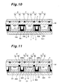
- Fig. 10 is a sectional view illustrating a fourth embodiment of the plasma displaypanel (PDP) according to the present invention, which is taken along the same line as that in Fig. 5 of the first embodiment.
- PDP plasma displaypanel
- the PDP in the fourth embodiment has an additional dielectric layer 42A constituted of a black- or dark-colored light absorption layer.
- Each of the additional dielectric layers 42A is formed on the back face of a dielectric layer 42 covering the row electrode pairs (X, Y) on the front glass substrate 1, in a position opposite the adjacent bus electrodes Xb and Yb of the respective row electrode pairs (X, Y) positioned alongside each other, and opposite the area between the adjacent bus electrodes Xb and Yb concerned, and extends in parallel to the bus electrodes Xb and Yb.
- the additional dielectric layer 42A is opposite to the back-to-back transverse walls 16A of the respective partition walls 16 and also to the interstice SL1 interposed between the transverse walls 16A concerned.
- the structure relating to the other elements in the fourth embodiment is similar to those of the PDPs in the first embodiment and the conventional example described in Description of the Related Art. Therefore the same elements as those in the first embodiment and the conventional example are designated with the same reference numerals, respectively.
- the PDP in the fourth embodiment is able to offer further close-to-perfect prevention of the reflection of the ambient light which has entered the non-light emission area of the panel, because the light absorption layer constitutes the additional dielectric layer 42A formed opposite the two back-to-back transverse walls 16A of the respective partition walls 16 and the interstice SL1 formed between the transverse walls 16A concerned to cover the non-light emission area between the adjacent display lines in which the transverse walls 16A and the corresponding interstice SL1 are placed.
- Fig. 11 illustrates a sectional view of a fifth embodiment of the plasma display panel (PDP) according to the present invention, which is taken along the same line as that of Fig. 7 of the second embodiment.
- PDP plasma display panel
- a partition wall 26 of the PDP in the fifth embodiment has similar structure to that in the second embodiment.
- the interstice formed between the transverse walls 26A in between the adjacent display lines is partitioned at regular intervals by the wall portions 26Ba of the vertical walls 26B each extending in the column direction.
- the PDP of the fifth embodiment includes spaces C2 each defined by the wall portions 26Ba partitioning the above interstice, and discharge cells C1 each formed opposite the paired transparent electrodes Xa and Ya in each row electrode pair (X, Y).
- the space C2 and the discharge cell C1 adjacent to the space C2 concerned in the column direction are paired with each other so that the discharge cell C1 constitutes a display discharge cell for producing a sustaining emission discharge, and the space C2 constitutesan addressing discharge cellfor producing anaddressing discharge.
- Each of additional dielectric layers 52A is formed opposite one of the two transverse walls 26A situated, in the column direction, on opposite sides of the space (addressing discharge cell) C2 defined in the interstice between the transverse walls 26A.
- the additional dielectric layer 52A extends in a belt shape in the row direction (a direction at right angles to Fig. 11), and protrudes from a dielectric layer 52, covering the row electrode pairs (X, Y), to come in contact with the transverse wall 26A.
- a pair of the display discharge cell C1 and addressing discharge cell C2 is shielded from another pair of the cells C1 and C2 adjacent thereto in the column direction by the additional dielectric layer 52A.
- the additional dielectric layer 52A is formed of a black- or dark-colored light absorption layer.
- the structure relating to the other elements in the fifth embodiment is similar to those of the PDP in the second embodiment. Therefore the same elements as those in the second embodiment are designated with the same reference numerals.
- the light absorption layer 20 is also formed in the addressing discharge cell C2. This makes it possible to prevent the reflection of the ambient light which has entered the inside of the addressing discharge cell C2.
- the additional dielectric layer 52A is formed of the black- or dark-colored light absorption layer to make it possible to offer further close-to-perfectprevention of the reflection of the ambient light which has entered the non-light emission area of the panel in which the addressing discharge cell C2 is placed.
- the light absorption layer 20 formed in the addressing discharge cell C2 may contain a material of a high coefficient of secondary electron emission, namely, a high r material of a low work function.
- the light absorption layer 20 blocks the reflection of the ambient light having entered the inside of the addressing discharge cell C2.
- the material having a high coefficient of secondary electron emission and contained in the light absorption layer 20 it is possible to reduce the discharge starting voltage for addressing discharge generated between the row electrode and the column electrode in the addressing discharge cell C2.
- Examples of such materials having a high coefficient of secondary electron emission include a material having a work function of 4.2 eV or less, such as: oxides of alkali metals (e.g. Cs 2 O: work function 2.3 eV); oxides of alkali-earth metals (e.g. CaO, SrO, BaO); fluorides (e. g. CaF 2 , MgF 2 ); a material increased in a coefficient of secondary electron emission by means of imperfection levels produced in crystal by crystal defects, impurities, or the like (e.g. MgOx having a composition ratio of Mg:O changed from 1:1 to cause crystal defects); TiO 2 ; Y 2 O 3 ; and so on.
- oxides of alkali metals e.g. Cs 2 O: work function 2.3 eV
- oxides of alkali-earth metals e.g. CaO, SrO, BaO
- fluorides e. g. CaF 2 , Mg
- a plasma display panel is structured such that a front substrate and a back substrate are opposite each other with a discharge space in between, a plurality of row electrode pairs are regularly arranged in a column direction and each extend in a row direction to form a display line, the plurality of row electrode pairs and a dielectric layer covering the row electrode pairs are formed on the front substrate, a plurality of column electrodes are regularly arranged on one of the back substrate and the front substrate in the row direction and each extend in the column direction to form unit light-emission areas at the intersections with the row electrode pairs in the discharge space, and the adjacent unit light-emission areas in the column direction are defined and separated from each other by transverse walls (extending in the row direction) of partition walls provided between the front substrate and the back substrate, and in the PDP, a black- or dark-colored light absorption layer facing the front substrate is formed in each area including the transverse walls between the unit light-emission areas
- each of the unit light-emission areas is formed in the discharge space at the intersection of the row electrode pair and the column electrode, the transverse wall of the partition wall provided inside the discharge space extends in the row direction and defines and separates the unit light-emission areas adjacent to each other in the column direction from each other.
- a black- or dark-colored light absorption layer is formed facing toward the front substrate.
- the light absorption layer is formed, in between the adjacent unit light-emission areas in the column direction, within the interstice between the adjacent transverse walls respectively partitioning off the unit light-emission areas or on the face of the transverse wall opposite the front substrate.
- the light is absorbed by the light absorption layer formed, facing toward the front substrate, in the non-light emission area in the discharge space, and thus the reflection of the light toward the front substrate is prevented.
- the PDP is capable of achieving improved contrast of images displayed on its screen without impairment caused by the reflection of the ambient light coming from the non-light emission area.
Landscapes
- Physics & Mathematics (AREA)
- Engineering & Computer Science (AREA)
- Plasma & Fusion (AREA)
- Electromagnetism (AREA)
- Gas-Filled Discharge Tubes (AREA)
Applications Claiming Priority (2)
| Application Number | Priority Date | Filing Date | Title |
|---|---|---|---|
| JP2002291816A JP2004127785A (ja) | 2002-10-04 | 2002-10-04 | プラズマディスプレイパネル |
| JP2002291816 | 2002-10-04 |
Publications (2)
| Publication Number | Publication Date |
|---|---|
| EP1406288A2 true EP1406288A2 (de) | 2004-04-07 |
| EP1406288A3 EP1406288A3 (de) | 2007-08-29 |
Family
ID=31987199
Family Applications (1)
| Application Number | Title | Priority Date | Filing Date |
|---|---|---|---|
| EP03022274A Withdrawn EP1406288A3 (de) | 2002-10-04 | 2003-10-01 | Plasma Anzeigetafel |
Country Status (3)
| Country | Link |
|---|---|
| US (1) | US6979950B2 (de) |
| EP (1) | EP1406288A3 (de) |
| JP (1) | JP2004127785A (de) |
Cited By (5)
| Publication number | Priority date | Publication date | Assignee | Title |
|---|---|---|---|---|
| EP1308982A3 (de) * | 2001-11-05 | 2005-12-07 | Lg Electronics Inc. | Plasma-Anzeigetafel und Herstellungsverfahren davon |
| EP1863061A2 (de) | 2006-05-30 | 2007-12-05 | LG Electronics Inc. | Plasmaanzeigevorrichtung |
| EP1876476A3 (de) * | 2006-07-07 | 2008-01-23 | Samsung Electronics Co., Ltd. | Anzeigetafel |
| EP1906431A3 (de) * | 2006-09-29 | 2008-08-27 | Fujitsu Hitachi Plasma Display Limited | Plasmaanzeigetafel |
| EP2184762A1 (de) * | 2008-11-10 | 2010-05-12 | Samsung SDI Co., Ltd. | Plasmaanzeigetafel |
Families Citing this family (7)
| Publication number | Priority date | Publication date | Assignee | Title |
|---|---|---|---|---|
| KR20050104215A (ko) * | 2004-04-28 | 2005-11-02 | 삼성에스디아이 주식회사 | 플라즈마 디스플레이 패널 |
| US7482754B2 (en) | 2004-08-13 | 2009-01-27 | Samsung Sdi Co., Ltd. | Plasma display panel |
| KR100626067B1 (ko) | 2005-03-22 | 2006-09-20 | 삼성에스디아이 주식회사 | 플라즈마 디스플레이 패널 |
| JP2006310280A (ja) * | 2005-03-31 | 2006-11-09 | Toray Ind Inc | プラズマディスプレイ用背面板およびプラズマディスプレイパネル |
| CN101449351A (zh) * | 2006-06-27 | 2009-06-03 | 日立等离子显示器股份有限公司 | 改善排气流导的等离子体显示面板 |
| KR100811604B1 (ko) | 2006-08-18 | 2008-03-11 | 엘지전자 주식회사 | 플라즈마 디스플레이 장치 |
| KR100814828B1 (ko) * | 2006-10-11 | 2008-03-20 | 삼성에스디아이 주식회사 | 플라즈마 디스플레이 패널 |
Family Cites Families (10)
| Publication number | Priority date | Publication date | Assignee | Title |
|---|---|---|---|---|
| JP3599316B2 (ja) | 1999-04-26 | 2004-12-08 | パイオニア株式会社 | プラズマディスプレイパネル |
| JP3594857B2 (ja) * | 1999-11-26 | 2004-12-02 | パイオニア株式会社 | プラズマディスプレイパネル |
| JP2002150949A (ja) * | 2000-11-09 | 2002-05-24 | Pioneer Electronic Corp | プラズマディスプレイパネル |
| US6614183B2 (en) * | 2000-02-29 | 2003-09-02 | Pioneer Corporation | Plasma display panel and method of manufacturing the same |
| JP4069583B2 (ja) * | 2000-03-28 | 2008-04-02 | 三菱電機株式会社 | プラズマディスプレイ装置 |
| KR100469175B1 (ko) * | 2000-11-28 | 2005-02-02 | 미쓰비시덴키 가부시키가이샤 | 플라즈마 디스플레이 패널 |
| KR100370738B1 (ko) * | 2000-12-29 | 2003-02-05 | 엘지전자 주식회사 | 플라즈마 디스플레이 패널 |
| US6674238B2 (en) * | 2001-07-13 | 2004-01-06 | Pioneer Corporation | Plasma display panel |
| JP3918992B2 (ja) * | 2002-01-30 | 2007-05-23 | 株式会社日立プラズマパテントライセンシング | プラズマディスプレイパネル用背面基板の製造方法 |
| JP2004200040A (ja) * | 2002-12-19 | 2004-07-15 | Pioneer Electronic Corp | プラズマディスプレイパネル |
-
2002
- 2002-10-04 JP JP2002291816A patent/JP2004127785A/ja not_active Abandoned
-
2003
- 2003-09-30 US US10/673,158 patent/US6979950B2/en not_active Expired - Fee Related
- 2003-10-01 EP EP03022274A patent/EP1406288A3/de not_active Withdrawn
Cited By (15)
| Publication number | Priority date | Publication date | Assignee | Title |
|---|---|---|---|---|
| US7821206B2 (en) | 2001-11-05 | 2010-10-26 | Lg Electronics Inc. | Plasma display panel and manufacturing method thereof |
| US7030561B2 (en) | 2001-11-05 | 2006-04-18 | Lg Electronics Inc. | Plasma display panel |
| US7040946B2 (en) | 2001-11-05 | 2006-05-09 | Lg Electronics Inc. | Plasma display panel and manufacturing method thereof |
| US7075236B2 (en) | 2001-11-05 | 2006-07-11 | Lg Electronics Inc. | Plasma display panel and manufacturing method thereof |
| EP1763054A3 (de) * | 2001-11-05 | 2007-07-18 | LG Electronics Inc. | Plasma-Anzeigetafel und deren Herstellungsverfahren |
| EP1308982A3 (de) * | 2001-11-05 | 2005-12-07 | Lg Electronics Inc. | Plasma-Anzeigetafel und Herstellungsverfahren davon |
| EP1863061A2 (de) | 2006-05-30 | 2007-12-05 | LG Electronics Inc. | Plasmaanzeigevorrichtung |
| EP1863061A3 (de) * | 2006-05-30 | 2008-03-19 | LG Electronics Inc. | Plasmaanzeigevorrichtung |
| US7852001B2 (en) | 2006-05-30 | 2010-12-14 | Lg Electronics Inc. | Plasma display apparatus |
| EP1876476A3 (de) * | 2006-07-07 | 2008-01-23 | Samsung Electronics Co., Ltd. | Anzeigetafel |
| US7745996B2 (en) | 2006-07-07 | 2010-06-29 | Samsung Electronics Co., Ltd. | Display panel film having a black layer and a reflective layer |
| US7755284B2 (en) | 2006-09-29 | 2010-07-13 | Fujitsu Hitachi Plasma Display Limited | Plasma display panel |
| EP1906431A3 (de) * | 2006-09-29 | 2008-08-27 | Fujitsu Hitachi Plasma Display Limited | Plasmaanzeigetafel |
| EP2184762A1 (de) * | 2008-11-10 | 2010-05-12 | Samsung SDI Co., Ltd. | Plasmaanzeigetafel |
| US8004191B2 (en) | 2008-11-10 | 2011-08-23 | Samsung Sdi Co., Ltd. | Plasma display panel |
Also Published As
| Publication number | Publication date |
|---|---|
| JP2004127785A (ja) | 2004-04-22 |
| EP1406288A3 (de) | 2007-08-29 |
| US6979950B2 (en) | 2005-12-27 |
| US20040189203A1 (en) | 2004-09-30 |
Similar Documents
| Publication | Publication Date | Title |
|---|---|---|
| US6700323B2 (en) | Plasma display panel | |
| US20010011871A1 (en) | Plasma display panel | |
| US6639363B2 (en) | Plasma display panel | |
| US7012370B2 (en) | Plasma display device with shielding parts on transparent electrodes | |
| US6979950B2 (en) | Plasma display panel configured to substantially block the reflection of light which enters a non-light emission area of the plasma display panel | |
| EP1326263A2 (de) | Plasma Anzeigetafel | |
| US7038382B2 (en) | Plasma display panel with offset discharge electrodes | |
| EP1376643A2 (de) | Plasmaanzeigetafel | |
| KR100842979B1 (ko) | 플라즈마 디스플레이 장치 | |
| US7663317B2 (en) | Plasma display panel | |
| US6995512B2 (en) | Plasma display panel | |
| JP2001155645A (ja) | プラズマディスプレイパネル | |
| US6628076B2 (en) | Plasma display panel | |
| KR100581922B1 (ko) | 투과형 플라즈마 디스플레이 패널 | |
| US20050285530A1 (en) | Plasma display panel | |
| JP3701823B2 (ja) | プラズマディスプレイパネル | |
| US20060012303A1 (en) | Plasma display panel | |
| US7719190B2 (en) | Plasma display panel | |
| KR100590079B1 (ko) | 플라즈마 디스플레이 패널 | |
| US20060001376A1 (en) | Plasma display panel | |
| US20070152912A1 (en) | Plasma display panel without transparent electrodes | |
| US20070228979A1 (en) | Plasma display panel | |
| KR20060063169A (ko) | 플라즈마 디스플레이 패널 | |
| JP2004355841A (ja) | プラズマディスプレイパネル | |
| KR20080044026A (ko) | 플라즈마 디스플레이 패널 |
Legal Events
| Date | Code | Title | Description |
|---|---|---|---|
| PUAI | Public reference made under article 153(3) epc to a published international application that has entered the european phase |
Free format text: ORIGINAL CODE: 0009012 |
|
| AK | Designated contracting states |
Kind code of ref document: A2 Designated state(s): AT BE BG CH CY CZ DE DK EE ES FI FR GB GR HU IE IT LI LU MC NL PT RO SE SI SK TR |
|
| AX | Request for extension of the european patent |
Extension state: AL LT LV MK |
|
| PUAL | Search report despatched |
Free format text: ORIGINAL CODE: 0009013 |
|
| AK | Designated contracting states |
Kind code of ref document: A3 Designated state(s): AT BE BG CH CY CZ DE DK EE ES FI FR GB GR HU IE IT LI LU MC NL PT RO SE SI SK TR |
|
| AX | Request for extension of the european patent |
Extension state: AL LT LV MK |
|
| STAA | Information on the status of an ep patent application or granted ep patent |
Free format text: STATUS: THE APPLICATION HAS BEEN WITHDRAWN |
|
| 18W | Application withdrawn |
Effective date: 20070904 |