EP1406308A2 - SiGeC Heteroübergang-Bipolartransistor - Google Patents
SiGeC Heteroübergang-Bipolartransistor Download PDFInfo
- Publication number
- EP1406308A2 EP1406308A2 EP03011764A EP03011764A EP1406308A2 EP 1406308 A2 EP1406308 A2 EP 1406308A2 EP 03011764 A EP03011764 A EP 03011764A EP 03011764 A EP03011764 A EP 03011764A EP 1406308 A2 EP1406308 A2 EP 1406308A2
- Authority
- EP
- European Patent Office
- Prior art keywords
- layer
- sigec
- emitter
- cap layer
- base
- Prior art date
- Legal status (The legal status is an assumption and is not a legal conclusion. Google has not performed a legal analysis and makes no representation as to the accuracy of the status listed.)
- Withdrawn
Links
Images


Classifications
-
- H—ELECTRICITY
- H10—SEMICONDUCTOR DEVICES; ELECTRIC SOLID-STATE DEVICES NOT OTHERWISE PROVIDED FOR
- H10D—INORGANIC ELECTRIC SEMICONDUCTOR DEVICES
- H10D10/00—Bipolar junction transistors [BJT]
- H10D10/01—Manufacture or treatment
- H10D10/021—Manufacture or treatment of heterojunction BJTs [HBT]
-
- H—ELECTRICITY
- H10—SEMICONDUCTOR DEVICES; ELECTRIC SOLID-STATE DEVICES NOT OTHERWISE PROVIDED FOR
- H10D—INORGANIC ELECTRIC SEMICONDUCTOR DEVICES
- H10D10/00—Bipolar junction transistors [BJT]
- H10D10/80—Heterojunction BJTs
- H10D10/821—Vertical heterojunction BJTs
- H10D10/891—Vertical heterojunction BJTs comprising lattice-mismatched active layers, e.g. SiGe strained-layer transistors
Definitions
- SiGe-HBT SiGe hetero-bipolar transistor
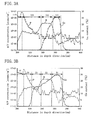
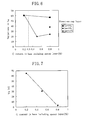
- the Ge mole fraction y2 in the direct-on cap layer is preferably 0.08 or less.
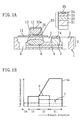
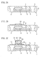
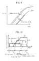
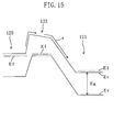
- an emitter/base stacked portion 20 obtained by stacking SiGeC and Si layers. This schematic structure of the SiGeC-HBT has been conventionally known.
- the direct-on cap layer is formed from not a SiGe cap layer but a SiGeC cap layer, barriers between the emitter and the base in the conduction band E c and between the base and the emitter in the valence band E v can be also reduced. Accordingly, the effects of the present invention can be achieved.
Landscapes
- Bipolar Transistors (AREA)
Applications Claiming Priority (2)
| Application Number | Priority Date | Filing Date | Title |
|---|---|---|---|
| JP2002292662 | 2002-10-04 | ||
| JP2002292662A JP3507830B1 (ja) | 2002-10-04 | 2002-10-04 | 半導体装置 |
Publications (2)
| Publication Number | Publication Date |
|---|---|
| EP1406308A2 true EP1406308A2 (de) | 2004-04-07 |
| EP1406308A3 EP1406308A3 (de) | 2004-10-13 |
Family
ID=31987222
Family Applications (1)
| Application Number | Title | Priority Date | Filing Date |
|---|---|---|---|
| EP03011764A Withdrawn EP1406308A3 (de) | 2002-10-04 | 2003-05-23 | SiGeC Heteroübergang-Bipolartransistor |
Country Status (4)
| Country | Link |
|---|---|
| US (1) | US6847062B2 (de) |
| EP (1) | EP1406308A3 (de) |
| JP (1) | JP3507830B1 (de) |
| TW (1) | TW200406046A (de) |
Cited By (2)
| Publication number | Priority date | Publication date | Assignee | Title |
|---|---|---|---|---|
| EP2346070A1 (de) | 2010-01-13 | 2011-07-20 | Nxp B.V. | Verfahren zur Herstellung eines bipolaren Heteroübertragungstransistors und bipolarer Heteroübertragungstransistor |
| US9105677B2 (en) | 2013-10-22 | 2015-08-11 | International Business Machines Corporation | Base profile of self-aligned bipolar transistors for power amplifier applications |
Families Citing this family (11)
| Publication number | Priority date | Publication date | Assignee | Title |
|---|---|---|---|---|
| US7517768B2 (en) * | 2003-03-31 | 2009-04-14 | Intel Corporation | Method for fabricating a heterojunction bipolar transistor |
| JP4775688B2 (ja) * | 2004-07-16 | 2011-09-21 | オンセミコンダクター・トレーディング・リミテッド | 半導体装置 |
| JP4850398B2 (ja) * | 2004-08-31 | 2012-01-11 | 株式会社日立製作所 | 半導体装置及びその製造方法 |
| US7002190B1 (en) * | 2004-09-21 | 2006-02-21 | International Business Machines Corporation | Method of collector formation in BiCMOS technology |
| US7170083B2 (en) * | 2005-01-07 | 2007-01-30 | International Business Machines Corporation | Bipolar transistor with collector having an epitaxial Si:C region |
| KR100781905B1 (ko) | 2006-10-25 | 2007-12-04 | 한국전자통신연구원 | 헤테로 정션 바이폴라 트랜지스터를 포함하는 이미지 센서및 그 제조 방법 |
| US20080128749A1 (en) * | 2006-12-01 | 2008-06-05 | Darwin Gene Enicks | Method and system for providing a drift coupled device |
| JP2008235560A (ja) | 2007-03-20 | 2008-10-02 | Matsushita Electric Ind Co Ltd | ヘテロ接合バイポーラトランジスタ |
| US20130307122A1 (en) * | 2012-05-16 | 2013-11-21 | Tsinghua University | Bipolar transistor with embedded epitaxial external base region and method of forming the same |
| US9502565B2 (en) * | 2014-06-27 | 2016-11-22 | Taiwan Semiconductor Manufacturing Company, Ltd. | Channel strain control for nonplanar compound semiconductor devices |
| US11955374B2 (en) * | 2021-08-29 | 2024-04-09 | Taiwan Semiconductor Manufacturing Company, Ltd. | Method for forming SOI substrate |
Family Cites Families (6)
| Publication number | Priority date | Publication date | Assignee | Title |
|---|---|---|---|---|
| DE60042045D1 (de) | 1999-06-22 | 2009-06-04 | Panasonic Corp | Heteroübergangsbipolartransistoren und entsprechende Herstellungsverfahren |
| JP2001332563A (ja) | 2000-05-23 | 2001-11-30 | Matsushita Electric Ind Co Ltd | バイポーラトランジスタ及びその製造方法 |
| JP2001338930A (ja) * | 2000-05-29 | 2001-12-07 | Nec Corp | 半導体装置および半導体製造方法 |
| JP3415608B2 (ja) | 2000-09-11 | 2003-06-09 | 松下電器産業株式会社 | ヘテロバイポーラトランジスタ |
| US20020163013A1 (en) * | 2000-09-11 | 2002-11-07 | Kenji Toyoda | Heterojunction bipolar transistor |
| US6441462B1 (en) * | 2001-07-10 | 2002-08-27 | International Business Machines Corporation | Self-aligned SiGe NPN with improved ESD robustness using wide emitter polysilicon extension |
-
2002
- 2002-10-04 JP JP2002292662A patent/JP3507830B1/ja not_active Expired - Lifetime
-
2003
- 2003-04-15 US US10/413,305 patent/US6847062B2/en not_active Expired - Lifetime
- 2003-05-09 TW TW092112699A patent/TW200406046A/zh unknown
- 2003-05-23 EP EP03011764A patent/EP1406308A3/de not_active Withdrawn
Cited By (5)
| Publication number | Priority date | Publication date | Assignee | Title |
|---|---|---|---|---|
| EP2346070A1 (de) | 2010-01-13 | 2011-07-20 | Nxp B.V. | Verfahren zur Herstellung eines bipolaren Heteroübertragungstransistors und bipolarer Heteroübertragungstransistor |
| US8242500B2 (en) | 2010-01-13 | 2012-08-14 | Nxp B.V. | Method of manufacturing heterojunction bipolar transistor and heterojunction bipolar transistor |
| US8524551B2 (en) | 2010-01-13 | 2013-09-03 | Nxp B.V. | Method of manufacturing heterojunction bipolar transistor and heterojunction bipolar transistor |
| US9105677B2 (en) | 2013-10-22 | 2015-08-11 | International Business Machines Corporation | Base profile of self-aligned bipolar transistors for power amplifier applications |
| US9269787B2 (en) | 2013-10-22 | 2016-02-23 | Globalfoundries U.S. 2 Llc | Base profile of self-aligned bipolar transistors for power amplifier applications |
Also Published As
| Publication number | Publication date |
|---|---|
| JP2004128343A (ja) | 2004-04-22 |
| US20040065875A1 (en) | 2004-04-08 |
| TW200406046A (en) | 2004-04-16 |
| US6847062B2 (en) | 2005-01-25 |
| JP3507830B1 (ja) | 2004-03-15 |
| EP1406308A3 (de) | 2004-10-13 |
Similar Documents
| Publication | Publication Date | Title |
|---|---|---|
| EP1065728B1 (de) | Heteroübergangsbipolartransistoren und entsprechende Herstellungsverfahren | |
| EP1187218B1 (de) | Heteroübergangsbipolartransistor | |
| KR100570910B1 (ko) | 인듐이 도핑된 베이스를 갖는 실리콘 게르마늄 헤테로구조 바이폴라 트랜지스터 | |
| US6847062B2 (en) | Semiconductor device | |
| US7420228B2 (en) | Bipolar transistor comprising carbon-doped semiconductor | |
| US20100283084A1 (en) | Bipolar transistor and method for fabricating the same | |
| KR100455829B1 (ko) | 초자기정렬 이종접합 바이폴라 소자 및 그 제조방법 | |
| JP3515944B2 (ja) | ヘテロバイポーラトランジスタ | |
| US6506659B2 (en) | High performance bipolar transistor | |
| US7170112B2 (en) | Graded-base-bandgap bipolar transistor having a constant—bandgap in the base | |
| US7579635B2 (en) | Heterojunction bipolar transistor | |
| US6847063B2 (en) | Semiconductor device | |
| US6972441B2 (en) | Silicon germanium heterojunction bipolar transistor with step-up carbon profile | |
| JP2002158232A (ja) | ヘテロバイポーラトランジスタ | |
| JP2007281096A (ja) | 半導体装置の製造方法およびエミッタポリシリコン電極構造をもつバイポーラトランジスタの電流増幅率の調整方法 |
Legal Events
| Date | Code | Title | Description |
|---|---|---|---|
| PUAI | Public reference made under article 153(3) epc to a published international application that has entered the european phase |
Free format text: ORIGINAL CODE: 0009012 |
|
| AK | Designated contracting states |
Kind code of ref document: A2 Designated state(s): AT BE BG CH CY CZ DE DK EE ES FI FR GB GR HU IE IT LI LU MC NL PT RO SE SI SK TR |
|
| AX | Request for extension of the european patent |
Extension state: AL LT LV MK |
|
| PUAL | Search report despatched |
Free format text: ORIGINAL CODE: 0009013 |
|
| AK | Designated contracting states |
Kind code of ref document: A3 Designated state(s): AT BE BG CH CY CZ DE DK EE ES FI FR GB GR HU IE IT LI LU MC NL PT RO SE SI SK TR |
|
| AX | Request for extension of the european patent |
Extension state: AL LT LV MK |
|
| RIC1 | Information provided on ipc code assigned before grant |
Ipc: 7H 01L 21/331 B Ipc: 7H 01L 29/161 B Ipc: 7H 01L 29/737 A |
|
| 17P | Request for examination filed |
Effective date: 20050303 |
|
| AKX | Designation fees paid |
Designated state(s): DE FR IT |
|
| 17Q | First examination report despatched |
Effective date: 20070606 |
|
| RAP1 | Party data changed (applicant data changed or rights of an application transferred) |
Owner name: PANASONIC CORPORATION |
|
| STAA | Information on the status of an ep patent application or granted ep patent |
Free format text: STATUS: THE APPLICATION IS DEEMED TO BE WITHDRAWN |
|
| 18D | Application deemed to be withdrawn |
Effective date: 20091201 |