EP1408511A1 - Nichtflüchtige Ein-Bit-Speicherzelle und Verfahren zu ihrem Programmieren und Löschen - Google Patents
Nichtflüchtige Ein-Bit-Speicherzelle und Verfahren zu ihrem Programmieren und Löschen Download PDFInfo
- Publication number
- EP1408511A1 EP1408511A1 EP20030447246 EP03447246A EP1408511A1 EP 1408511 A1 EP1408511 A1 EP 1408511A1 EP 20030447246 EP20030447246 EP 20030447246 EP 03447246 A EP03447246 A EP 03447246A EP 1408511 A1 EP1408511 A1 EP 1408511A1
- Authority
- EP
- European Patent Office
- Prior art keywords
- voltage
- region
- drain
- memory cell
- applying
- Prior art date
- Legal status (The legal status is an assumption and is not a legal conclusion. Google has not performed a legal analysis and makes no representation as to the accuracy of the status listed.)
- Withdrawn
Links
- 230000015654 memory Effects 0.000 title claims abstract description 109
- 238000000034 method Methods 0.000 title claims description 44
- 239000000758 substrate Substances 0.000 claims abstract description 29
- 239000000969 carrier Substances 0.000 claims abstract description 28
- 238000002347 injection Methods 0.000 claims abstract description 25
- 239000007924 injection Substances 0.000 claims abstract description 25
- 239000004065 semiconductor Substances 0.000 claims description 24
- 238000005516 engineering process Methods 0.000 claims description 16
- 230000007246 mechanism Effects 0.000 claims description 15
- 238000003860 storage Methods 0.000 claims description 11
- 150000004767 nitrides Chemical class 0.000 claims description 8
- 230000002441 reversible effect Effects 0.000 claims description 3
- 230000002093 peripheral effect Effects 0.000 claims 1
- 230000002829 reductive effect Effects 0.000 abstract description 2
- 239000002784 hot electron Substances 0.000 description 7
- 229910021420 polycrystalline silicon Inorganic materials 0.000 description 7
- VYPSYNLAJGMNEJ-UHFFFAOYSA-N Silicium dioxide Chemical compound O=[Si]=O VYPSYNLAJGMNEJ-UHFFFAOYSA-N 0.000 description 6
- XUIMIQQOPSSXEZ-UHFFFAOYSA-N Silicon Chemical compound [Si] XUIMIQQOPSSXEZ-UHFFFAOYSA-N 0.000 description 5
- 230000004888 barrier function Effects 0.000 description 5
- 230000008901 benefit Effects 0.000 description 5
- 239000002184 metal Substances 0.000 description 5
- 229910052710 silicon Inorganic materials 0.000 description 5
- 239000010703 silicon Substances 0.000 description 5
- 230000006870 function Effects 0.000 description 4
- 230000008569 process Effects 0.000 description 4
- 238000005229 chemical vapour deposition Methods 0.000 description 3
- 230000005684 electric field Effects 0.000 description 3
- 230000000873 masking effect Effects 0.000 description 3
- MCMNRKCIXSYSNV-UHFFFAOYSA-N Zirconium dioxide Chemical compound O=[Zr]=O MCMNRKCIXSYSNV-UHFFFAOYSA-N 0.000 description 2
- 230000001133 acceleration Effects 0.000 description 2
- 238000003491 array Methods 0.000 description 2
- 230000006399 behavior Effects 0.000 description 2
- 230000015572 biosynthetic process Effects 0.000 description 2
- 239000002800 charge carrier Substances 0.000 description 2
- 230000009977 dual effect Effects 0.000 description 2
- 230000014759 maintenance of location Effects 0.000 description 2
- 239000013081 microcrystal Substances 0.000 description 2
- 239000012811 non-conductive material Substances 0.000 description 2
- 239000000377 silicon dioxide Substances 0.000 description 2
- 229910052814 silicon oxide Inorganic materials 0.000 description 2
- 230000005689 Fowler Nordheim tunneling Effects 0.000 description 1
- 229910052581 Si3N4 Inorganic materials 0.000 description 1
- BOTDANWDWHJENH-UHFFFAOYSA-N Tetraethyl orthosilicate Chemical compound CCO[Si](OCC)(OCC)OCC BOTDANWDWHJENH-UHFFFAOYSA-N 0.000 description 1
- PNEYBMLMFCGWSK-UHFFFAOYSA-N aluminium oxide Inorganic materials [O-2].[O-2].[O-2].[Al+3].[Al+3] PNEYBMLMFCGWSK-UHFFFAOYSA-N 0.000 description 1
- 238000000277 atomic layer chemical vapour deposition Methods 0.000 description 1
- 230000015556 catabolic process Effects 0.000 description 1
- 230000008859 change Effects 0.000 description 1
- 229910052681 coesite Inorganic materials 0.000 description 1
- 239000004020 conductor Substances 0.000 description 1
- 229910052593 corundum Inorganic materials 0.000 description 1
- 229910052906 cristobalite Inorganic materials 0.000 description 1
- 238000013500 data storage Methods 0.000 description 1
- 230000007423 decrease Effects 0.000 description 1
- 230000003247 decreasing effect Effects 0.000 description 1
- 238000000151 deposition Methods 0.000 description 1
- 239000003989 dielectric material Substances 0.000 description 1
- 238000009792 diffusion process Methods 0.000 description 1
- 230000000694 effects Effects 0.000 description 1
- CJNBYAVZURUTKZ-UHFFFAOYSA-N hafnium(IV) oxide Inorganic materials O=[Hf]=O CJNBYAVZURUTKZ-UHFFFAOYSA-N 0.000 description 1
- 230000010354 integration Effects 0.000 description 1
- 238000004518 low pressure chemical vapour deposition Methods 0.000 description 1
- 238000004519 manufacturing process Methods 0.000 description 1
- 239000000463 material Substances 0.000 description 1
- 230000003647 oxidation Effects 0.000 description 1
- 238000007254 oxidation reaction Methods 0.000 description 1
- 229920005591 polysilicon Polymers 0.000 description 1
- 230000009467 reduction Effects 0.000 description 1
- 230000000717 retained effect Effects 0.000 description 1
- 238000012216 screening Methods 0.000 description 1
- 235000012239 silicon dioxide Nutrition 0.000 description 1
- HQVNEWCFYHHQES-UHFFFAOYSA-N silicon nitride Chemical compound N12[Si]34N5[Si]62N3[Si]51N64 HQVNEWCFYHHQES-UHFFFAOYSA-N 0.000 description 1
- 125000006850 spacer group Chemical group 0.000 description 1
- 229910052682 stishovite Inorganic materials 0.000 description 1
- 229910052905 tridymite Inorganic materials 0.000 description 1
- 230000005641 tunneling Effects 0.000 description 1
- 229910001845 yogo sapphire Inorganic materials 0.000 description 1
Images


Classifications
-
- G—PHYSICS
- G11—INFORMATION STORAGE
- G11C—STATIC STORES
- G11C16/00—Erasable programmable read-only memories
- G11C16/02—Erasable programmable read-only memories electrically programmable
- G11C16/04—Erasable programmable read-only memories electrically programmable using variable threshold transistors, e.g. FAMOS
- G11C16/0466—Erasable programmable read-only memories electrically programmable using variable threshold transistors, e.g. FAMOS comprising cells with charge storage in an insulating layer, e.g. metal-nitride-oxide-silicon [MNOS], silicon-oxide-nitride-oxide-silicon [SONOS]
-
- G—PHYSICS
- G11—INFORMATION STORAGE
- G11C—STATIC STORES
- G11C16/00—Erasable programmable read-only memories
- G11C16/02—Erasable programmable read-only memories electrically programmable
- G11C16/06—Auxiliary circuits, e.g. for writing into memory
- G11C16/10—Programming or data input circuits
- G11C16/12—Programming voltage switching circuits
-
- G—PHYSICS
- G11—INFORMATION STORAGE
- G11C—STATIC STORES
- G11C16/00—Erasable programmable read-only memories
- G11C16/02—Erasable programmable read-only memories electrically programmable
- G11C16/06—Auxiliary circuits, e.g. for writing into memory
- G11C16/10—Programming or data input circuits
- G11C16/14—Circuits for erasing electrically, e.g. erase voltage switching circuits
-
- G—PHYSICS
- G11—INFORMATION STORAGE
- G11C—STATIC STORES
- G11C16/00—Erasable programmable read-only memories
- G11C16/02—Erasable programmable read-only memories electrically programmable
- G11C16/06—Auxiliary circuits, e.g. for writing into memory
- G11C16/26—Sensing or reading circuits; Data output circuits
Definitions
- the present invention generally relates to electrically programmable and erasable memory (EEPROM) devices, more particularly to single gate memory devices using a dielectric layer for locally storing and retaining a single bit of injected charge.
- EEPROM electrically programmable and erasable memory
- the present invention further particularly relates to methods for programming and erasing such memory devices at reduced voltages using hot-carrier injection.
- Flash EEPROM memories comprise the largest class of electrically alterable, nonvolatile semiconductor memories. They represent the fastest growing segment of all semiconductor memories, offering high integration densities, fast read access, electrical write and erase and allow a permanent data storage. Flash EEPROM memories offer the ability of erasing all or selected groups of the memory cells. Charge is stored on a floating gate, which modulates the conductance of a MOS channel underneath it. This floating gate is electrically insulated from its surroundings by a high quality dielectric, such as SiO 2 . A control gate, capacitively coupled to the floating gate, is used to modulate the electrical potential of the floating gate. The floating gate is formed from a conductive material such as polycrystalline silicon in which case injected charge will be distributed over the whole of the conductive floating gate.
- a non-conductive material such as nitride
- nitride can be used to store charge on.
- Charge introduced into the non-conductive gate will, to a large extent, be confined to the place of introduction and as a result only a limited amount of charge is needed to program the memory cell.
- PCT application WO 99/07000 discloses a two-bit non-volatile EEPROM cell using a nitride layer sandwiched in between a top and a bottom oxide layer. This memory cell is programmed using conventional channel-hot-electron-injection to inject electrons into the nitride layer.
- Channel-hot-electron-injection requires the junction region to overlap the nitride layer as the injection of the hot carriers occurs at the position of the maximum electrical field, which corresponds to the metallurgical junction between the drain and the well. Hence a sharp and well-controlled doping profile must be realized too.
- the symmetrical layout of the device allows, by appropriately selecting the voltages, electrons to be injected on either side of the non-conductive floating gate.
- Two bits of data can hence be stored, each bit on an opposite side of the floating gate. Erasing of the cell is done by removing the trapped electrons, through the top or the bottom electrode, using Fowler-Nordheim tunneling.
- the stored bits are read in "reverse direction": the bit at the drain side is read, i.e. the shift in threshold voltage at this point, is measured, by grounding the drain and biasing the source and the gate voltage such that saturation is reached in the channel region near the source. This saturation region will mask the influence of the charge, which is stored near the source junction.
- the doping profile must thus not only be engineered to enable localized injection of carriers, but also to allow screening of the bit on the opposite side of the one being sensed.
- the voltages required to program, read or write the cell must be compatible with the supply voltage of the logic circuitry on chip. Otherwise complex and area consuming charge pump circuits and high voltage circuits, which are e.g. used in the decoder circuitry, must be provided on chip to provide the internal or on-chip voltages needed to operate the flash memory.
- the scaling of the transistor dimensions towards 0.35 micrometer and below will however also scale down the available supply voltage from 5V towards 3.3V and below. Providing sufficient power to operate the memory cell becomes even more difficult when the supply voltage is scaled and the memory array density is increased, leaving less area for the column drivers. Furthermore the charge pump circuits, which generate the high memory operating voltages for programming and erasing from the low supply voltage, become less efficient and more area consuming as the supply voltage is decreased.
- An aim of the present invention is to allow low-voltage operation on-chip of an embedded flash EEPROM single gate memory cell and arrays thereof.
- An aim of the present invention is to disclose a low-voltage programming method for a single gate, single bit memory cell comprising a charge-storing dielectric.
- An aim of the present invention is to disclose a low-voltage programming method for a single poly single bit memory cell comprising a charge-storing dielectric.
- An aim of the present invention is to disclose a low-voltage erasing method for a single gate, single bit memory cell comprising a charge-storing dielectric.
- An aim of the present invention is to allow efficient use of chip-area, particularly when further downscaling the CMOS technology in which both the logic circuitry as well as the integrated EEPROM is manufactured.
- An aim of the present invention is to allow further downscaling of flash single bit memory cells using a layer of a non-conductive material as floating gate.
- Another aim of the present invention is to reduce the costs of integrating flash memory cells in a CMOS process. This is particularly important for so-called embedded memory applications where the process steps related to the manufacturing of the memory cells have to be reconciled with the available CMOS process for fabricating chips.
- Another aim of the invention is to disclose a memory cell concept that can be used for embedded Flash technology for wireless System-On-a-Chip applications.
- a single bit nonvolatile memory cell capable of being integrated on a chip in a metal-dielectric-semiconductor technology.
- This memory cell (1) comprising a semiconductor substrate (2) including a source (3), a drain (4), a channel region (10) in-between said source (3) and said drain (4), a gate electrode (5) separated from said channel region by a dielectric stack (6), said dielectric stack comprising at least one charge storing dielectric layer (8).
- a method for programming the single bit, single gate nonvolatile memory cell of the first aspect comprising a semiconductor substrate (2) including a source (3), a drain (4), a channel region (10) in-between said source (3) and said drain (4), a gate electrode (5) separated from said channel region by a dielectric stack (6), said dielectric stack comprising at least one charge storing dielectric layer (8).
- Said programming method comprising the steps of biasing said source (3) to ground, applying a first voltage of a first sign to said drain (4), applying a second voltage of a first sign to said gate (5), and applying a third voltage of an opposite sign to said semiconductor substrate (2), said first, said second and said third voltage cooperatively establishing programming of said cell using secondary-impact-ionization-carriers.
- the difference in absolute value of the first, second and third voltage being applied respectively to the drain, gate and bulk during programming is 1.5V or less, preferably 1V or less.
- the absolute value of the first, second and third voltage being applied respectively to the drain, gate and bulk during programming is about the same value. Preferably this absolute value is 5 V or less, more preferably this absolute value is 4.5V or less.
- a method for erasing a single bit, single gate nonvolatile memory cell according to the first aspect comprising a semiconductor substrate (2) including a source (3), a drain (4), a channel region 10 in-between said source (3) and said drain (4), a gate electrode (5) separated from said channel region by a dielectric stack (6), said dielectric stack comprising at least one charge storing dielectric layer (8).
- Said erasing method comprising the steps of biasing said source (3) to ground, applying a first voltage of a first sign to said drain (4), applying a second voltage of an opposite sign to said gate (5) and applying a third voltage of an opposite sign to said semiconductor substrate (2), said first, said second and said third voltage cooperatively establishing programming of said cell using band-to-band-tunneling-induced-hot-carrier injection.
- the difference in absolute value of the first, second and third voltage being applied respectively to the drain, gate and bulk during programming is of 1.5V or less, preferably 1V or less (Same remark as above).
- the absolute value of the first, second and third voltage being applied respectively to the drain, gate and bulk during programming is about the same value. Preferably this absolute value is 5 V or less, more preferably this absolute value is 4.5V or less.
- an efficient array configuration for the memory device is disclosed.
- the memory cells of the first aspect are organized in columns. Two adjacent memory cells in each column have either the drain (4) or the source (3) node in common
- the drain (4) nodes of two adjacent memory cells in each column are connected to form a program line PL, running perpendicular to the cell column.
- this program PL is formed in a first interconnect layer of metal connected via contacts or vias to the drain junction.
- the source nodes (3) of the memory cells in each column are connected to form a bit line, running parallel to the corresponding cell column.
- this bit line is formed in a second, higher, interconnect layer of metal connected via contacts or vias to the source junction.
- the gate (5) of memory cells at identical horizontal positions in each column are connected by the word line WL, running perpendicular to the cell column.
- this word line is formed in the polycrystalline silicon used to form the gate electrode (4) of each memory cell. So word lines and program lines are arranged in parallel.
- Figure 1 represents a schematic cross-sectional layout of a memory device according to the present invention
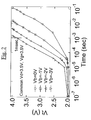
- Figure 2 represents programming characteristics of a device according to the present invention illustrating the threshold voltage window, and more particularly the influence of the substrate bias.
- Figure 3 represents a comparison of the bit-bit interference according the prior art (CHE) and the invention (SEHE).
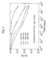
- Figure 4 represents erase characteristics of a device according to the present invention illustrating the threshold voltage window, and more particularly the influence of the substrate bias.
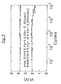
- Figure 5 represents endurance characteristic of a memory device programmed and erased according to embodiments of the invention.
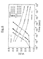
- Figure 6 represents cell performances when programming and erasing a memory device according to embodiments of the invention.
- Figure 7 represents a suitable memory array configuration for the memory device according to an embodiment of the invention.
- Figure 8 represents a program inhibit behavior of the memory architecture according to embodiments of the invention.
- supply voltage is meant the voltage used to supply power to any logic circuit on chip, fabricated in the CMOS technology in which the non-volatile memory cells are incorporated. Any externally applied voltage other than the supply voltage defined above will be referred to herein simply as an "external voltage”. With “internal voltage” is meant the voltage available on-chip, which is generated by charge pump circuits from the lower supply voltage.
- FIG. 1 shows a schematic cross-sectional layout of a single gate device (1) according to a first embodiment of this aspect.
- a semiconductor substrate (2) e.g. a silicon wafer
- source (3) and drain (4) highly doped junctions are formed self-aligned to a single gate, which comprises a conductive gate (5) formed on a stack (6) of dielectrics layers. Because the MOSFET structure available in the core CMOS technology is used, the junction regions (3) and (4) will essentially not overlap the gate region (5).
- a doped extension 4a (and potentially a lowly doped extension), underneath a spacer (12), can be present to form a conductive path between the highly doped junction (4b) and the channel region (10), as is common practice in submicron CMOS technology.
- the source (3) and drain (4) junctions are of a doping type opposite to the doping type of the substrate (1) or well.
- an n-channel device will be used wherein n-type junctions are thus formed in a p-type substrate or p-well.
- source and drain junction is meant the highly doped junction regions formed adjacent this single gate.
- the conductive gate (5) is used as gate electrode to bias the underlying FET structure.
- the underlying stack (6) of dielectric layers acts as the gate dielectric of this FET structure and can be a sandwich of a first (7), a second (8) and a third (9) dielectric layer.
- the first (7) and third (9) dielectric layers are electrically insulating the middle layer (8).
- This middle layer (8) is used as a charge trapping or charge-storing layer.
- the stack of dielectric layers must be capable of receiving charge carriers injected from the channel region (10) below. The injected charge carriers must be stored and retained within the non-conductive middle layer (8).
- the charge trapping layer (8) can be a nitride layer, an oxide layer with buried separated poly-silicon islands where the charge is stored within these conductive poly-silicon islands, a layer comprising separated silicon microcrystals, where the charge can be stored in these separated silicon microcrystals, a silicon-rich oxide, a high-k dielectric such as HfO 2 , Al 2 O 3 or ZrO 2 .
- the stack (6) of dielectric layers (7, 8, 9) can be formed by depositing a first dielectric (7) on top of a major surface of the semiconductor substrate (2).
- This first dielectric (7) is typically silicon dioxide formed by thermal oxidation of the silicon substrate (1) or can be deposited by a variety of CVD (chemical vapour deposition) techniques, e.g. TEOS formed by Low Pressure CVD, oxides formed by Atomic Layer CVD. Typically the thickness of this first dielectric is between 3 and 20 nm, preferably between 3 and 10nm.
- the second dielectric (8) is formed on top of the first dielectric (7), which electrically insulates this second dielectric (8) from the channel region ('10) underneath.
- the second dielectric (8) is a silicon nitride, having a thickness between 2 and 20 nm, preferably between 5 and 12nm.
- a third dielectric layer (9) is formed, e.g. by CVD, which electrically insulates the second dielectric (9) from the gate (5).
- this third dielectric (9) is a silicon oxide having a thickness between 3 and 20 nm, preferably between 3 and 10nm.
- the nitride layer (8) provides the charge retention mechanism for programming the memory cell.
- a conductive gate (5) is formed on top of the third dielectric layer (9) .
- polycrystalline silicon having a thickness ranging from 100 to 400 nanometer (nm) is used as gate material, in which case the device could be labeled as a single poly device.
- the conductive gate (5) will be of the same doping type as the source (3) and drain (4) junctions.
- the device shown in figure 1 comprises the MOSFET elements of a gate (5), source (3) and drain (4) terminals and a dielectric layer (6) separating the gate (5) from the channel region (10) in-between this source (3) and drain (4) region.
- This additional masking step is needed to remove the uniformly deposited non-conductive charge-storing layer outside the region on the chip allocated to the memory array.
- the formation of the dielectric stack (6) is first formed uniform over the wafer and, by using a masking step, then removed outside the memory region.
- the gate dielectric e.g.
- the gate electrode layer e.g. a polycrystalline layer, is deposited over the wafer. This gate electrode layer is patterned to form the gate of the logic devices as well as the gate of the memory cells. All other steps available in the core CMOS technology, and as such known by a person skilled in the art, can be further applied to complete the MOSFET structures of both the logic and of the memory part of the chip.
- Another advantage of the devices according to embodiments of the invention is that the proposed devices don't require elaborate junction engineering to ensure, inter alia, localised hot carrier injection.
- the thickness of the ONO stack (6) of this SONOS (semiconductor-ONO-semiconductor) device is 5.5nm for the bottom oxide (7), 8.5nm for the nitride layer (8), 5.5nm for the top oxide layer (9).
- the n-type source (3) and drain (4) junctions are 0.12um deep and formed in a retrograde well having a doping of 3e17 cm 2 .
- the cell size is 0.54 um 2 with a width over length ratio W/L of 0.25um/0.18um.
- the methods as disclosed in this patent application can be applied to any non-volatile memory technology embedded in a CMOS technology. A person skilled in the art will however appreciate the advantages of the embodiments presented when scaling down the CMOS technology, in which the non-volatile memory is integrated with logic circuitry, to submicron dimensions.
- a method for programming a single gate non-volatile memory cell comprising a charge-storing dielectric layer, as disclosed in the first aspect of the invention.
- the memory cell is programmed from the drain side, by applying a first voltage of a first sign to the drain junction (4), a second voltage of a first sign to the gate (5), a third voltage of an opposite sign to the substrate (2) and biasing the source junction (3) to ground.
- Primary carriers, electrons in this teaching, will then migrate from the source (3) through the channel 10 to the drain (4) (arrow i) and gain energy from the drain-source voltage thereby creating electron-hole pairs by a first impact ionisation mechanism in or near the drain.
- first-impact carriers which are holes in this teaching, will travel from the point of impact into the bulk (2) of the device (arrow j) and gain energy from the drain-bulk voltage thereby creating, in the bulk electron-hole pairs by a second impact ionisation event. Because the position where this second impact ionisation occurs depends on a number of parameters such as, inter-alia, the energy of the first-impact carriers, their diffusion life-time, the bulk doping, the doping profile and depth of the drain junction, one can not speak of an impact position but rather of an impact region as indicated by the cloud k.
- second-impact carriers which are electrons in this teaching, will be attracted towards the gate (5) by the gate voltage and will be injected near the drain side (4) into the dielectric stack (6) comprising the charge-storing dielectric (8) (arrows 1). Because of the statistical nature of this process, as indicated by the cloud k, the second-impact carriers will not be injected into the dielectric stack (6) at one single position along the channel as would be the case for classical hot-electron-injection, but at a statistically distributed set of points.
- the programming mechanism exploited in this embodiment charges the charge storing layer by a less-localized injection of hot carriers, generated by a secondary impact ionisation mechanism, taking place in the bulk of the device. Instead of having the majority of the injected charges stored at substantially the same location in the dielectric stack (6), the injected charge is distributed over a region within this dielectric stack, this region being determined by the statistics of the overall carrier generation process.
- the primary electrons will only need to gain enough energy to generate the first-impact carriers; a lower voltage difference between the source (3) and the drain (4) can be applied. Because the first-impact carriers must gain enough energy to generate second-impact carriers; a moderate voltage difference between the drain (4) and the substrate (2) can be applied. The gate (5) to substrate (2)-voltage must be large enough for the second-impact carriers to gain sufficient energy to cross the substrate-dielectric energy barrier. If oxide is used as a first dielectric (7) then this energy barrier is 3.2eV for electrons and 4.8eV for holes. For the device proposed by J.
- the injected charge is stored on a conductive floating gate and not on a non-conductive charge-storing dielectric (6) as disclosed in the embodiments of the invention.
- the gate electrode (5) In order to attract the generated carriers towards this floating gate Bude must apply a very high voltage to the gate electrode (5) as only a part of this gate voltage will be available at the floating gate due to the capacitive divider which is created between the substrate (2), the floating gate and the gate electrode (5).
- Such capacitive divider is not present in the device disclosed in the embodiments, allowing a lower gate (5) to substrate (2)-voltage.
- the difference in absolute value of the first and second being applied respectively to the drain, gate and bulk during programming is 1.5V or less, preferably 1V or less.
- the difference in absolute value of the first, second and third voltage being applied respectively to the drain, gate and bulk during programming is 1.5V or less, preferably 1V or less.
- the absolute value of the first, second and third voltage being applied respectively to the drain, gate and bulk during programming is about the same. Preferably this absolute value is 5 V or less, more preferably this absolute value is 4.5V or less.
- the drain is biased to 3.5V, the gate to 3.5V while the substrate is biased to -3V.
- the first and second voltage have a positive sign, while the third voltage has a negative sign.
- a more negative bulk bias will lead to an improved programming efficiency, as the threshold voltage shift after a given programming time, e.g. 1 msec, becomes larger with increasing bulk bias.
- the programming mechanism of the present invention is labelled as substrate-enhanced-hot-electron-injection (SEHE).
- SEHE substrate-enhanced-hot-electron-injection
- One feature of this programming mechanism is that, contrary to the conventional channel-hot-electron (CHE) mechanism, carriers are not injected into the floating gate (6) at a well-defined position.
- the injection of the carriers according to the present invention is a non-local injection phenomenon, showing a much more scattered injection behaviour.
- Figure 3 illustrates the difference between the present invention and channel-hot-electron with respect to the spread of the injection position when programming the device of figure 1.
- the change in threshold voltage ⁇ Vt (V) at the source side, being the "bit at the opposite side", of the transistor is monitored.
- the two bits are read, i.e. the shift in threshold voltage is measured at two values of the read voltage Vds between source and drain: 1V and 1.6V.
- CHE channel-hot-electron
- CHE channel-hot-electron
- the single bit device of this embodiment has an asymmetric charge storage mechanism: charge is stored from the drain side onwards, but is not located at the drain side only.
- a lower bit line read voltage e.g. 1V
- the read voltage e.g. 1.5V of the two-bit memory device of PCT application WO 99/07000
- the higher read-out voltage used in the prior art is required to extend the depletion region of the junction to mask the neighboring bit that is not being read out.
- this higher read-out voltage might result in a so-called soft write error: some carriers of the read-out current might gain enough energy to be injected into this masked bit and hence add unwanted charge to this bit..
- a method for erasing the single gate non-volatile memory cell (1) comprising a charge-storing dielectric layer as disclosed in the first aspect of the invention.
- the memory cell is erased from the drain side, by applying a first voltage of a first sign to the drain junction (4), a second voltage of an opposite sign to the program gate (4), a third voltage of an opposite sign to the substrate (1) and biasing the source junction (3) to ground.
- the erasing mechanism uses injection of hot carriers into the charge storing dielectric (8) near the drain side (4) of the memory cell (1). These carriers will be of an opposite type than the carriers used for programming, e.g. in this teaching electrons are injected during programming, while holes are injected during erasing.
- the drain (4) is put into deep depletion and "cold" holes can be generated by band-to-band tunnelling between the drain (4) and the channel region (10). These "cold" holes gain sufficient energy from the surface lateral electrical field to become hot and to cross the substrate-dielectric energy barrier. If oxide is used as a first dielectric (7) then this energy barrier is 3.2eV for electrons and 4.8eV for holes.
- the gate-drain voltage must be sufficient to form a deep depletion region at the drain side and allow band-to-band tunnelling of carriers used for erasing.
- the gate (5) to substrate (2)-voltage must be large enough for these carriers to gain sufficient energy to cross the substrate-dielectric energy barrier.
- the difference in absolute value of the first, second and third voltage being applied respectively to the drain, gate and bulk during programming is 1.5V or less, preferably 1V or less.
- the absolute value of the first, second and third voltage being applied respectively to the drain, gate and bulk during programming is about the same value. Preferably this absolute value is 5 V or less, more preferably this absolute value is 4.5V or less.
- the drain (4) is biased to 3.5V, the gate (5) to -3.5V while the substrate (2) is biased to -3V and the source (3) is put to 0V.
- the first voltage has a positive sign, while the second and third voltage have a negative sign. A more negative bulk bias will lead to an improved erase efficiency, as the threshold voltage shift after a given erase time becomes smaller with increasing bulk bias.
- the erasing mechanism of the present invention is labelled as substrate-enhanced-band-to-band-tunneling-induced-hot-hole-injection (SEBBHH).
- SEBBHH substrate-enhanced-band-to-band-tunneling-induced-hot-hole-injection
- SEBBHH substrate-enhanced-band-to-band-tunneling-induced-hot-hole-injection
- Figure 5 shows the endurance characteristics of the cell programmed and read according to embodiments of the invention. More than 100 000 cycles can be obtained.
- FIG. 7 shows a memory comprising several sectors. Black squares indicate the connection between a metal line, e.g. wordline(WL), bitline (BL), program line (PL), and a terminal, e.g. source (3), drain (4) or gate electrode (5).
- a metal line e.g. wordline(WL), bitline (BL), program line (PL), and a terminal, e.g. source (3), drain (4) or gate electrode (5).
- NOR-type memory array architecture according to one embodiment of the invention is shown.
- the memory cells are organized in columns. Two adjacent memory cells in each column have either the drain (4) or the source (3) node in common, e.g. it will have the source (3) in common with the memory cell (1) at one side and the drain node (4) in common with the memory cell at its opposite side.
- the drain (4) nodes of two adjacent memory cells in each column are connected, as indicated by the black squares in figure 7, to form a program line (PL), running perpendicular to the cell column.
- this program (PL) is formed in a first interconnect layer of metal connected via contacts or vias to the drain junction.
- the memory devices are mirrored with respect to the program metal.
- the source nodes (3) of the memory cells in each column are connected to form a bit line, running parallel to the corresponding cell column.
- this bit line is formed in a second, higher, interconnect layer of metal connected via contacts or vias to the source junction.
- From each column the gate (5) of memory cells at identical horizontal positions in each column are connected by the word line (WL), running perpendicular to the cell column.
- this word line is formed in the polycrystalline silicon used to form the gate electrode (4) of each memory cell. So word lines and program lines are arranged in parallel.
- the memory array shown in figure 7 is a contacted array as the source (3), drain (4) and gate (5) terminal of the individual memory cell is contacted. At each intersection of a wordline (WL) and a bitline (BL) a memory cell (1) is located.
- One advantage of the memory architecture according to this embodiment is that the highest voltage seen within one sector (11) at the drain (4) and the gate (5) of each cell can be limited, resulting in a high enough disturb margin.
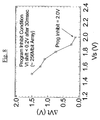
- Program inhibit is needed to prevent unwanted programming of memory cells. If for example the cell (1) at the intersection of column (C) and row (A) is to be programmed, the cells in row (A) belonging to the other columns (D, E, F) will be exposed to these drain and gate voltages. To prevent unwanted programming of these cells the respective other bitlines (BL: D, E, F) etc. will be biased, in this teaching, to a positive voltage.
- bitlines (BL) are common between sector (11) above and sector (12) below, the memory cells of sector (12) will be exposed to a higher voltage at their sources (3) , which might cause disturbance within these cells. Thanks to the low program voltage, e.g. less than 4.5V in the examples given above, the inhibit voltage applied at the source side (3) of the memory cells in column (D) can be low. Because, as shown in figure 7, the bit line (BL) connecting the source nodes (3) of a column is common to all sectors, the bias applied to the this bit line will be seen by all memory cells in each sector sharing this bit line. A too high source inhibit voltage would introduce disturb across other sectors.
- a source inhibit voltage Vs of 2V would be sufficient to prevent a significant shift (V) in threshold voltage Vt.
- V threshold voltage shift
- the threshold voltage shift decreases as function of the source voltage.
- a shift of less than 200mV can be obtained even the drain side is biased for 30 sec.
- the program time of memory array is about 20 milliseconds (msec): 1K word x 20usec/cell.
- the disturb time i.e. the time during which cells of the mirror row are exposed to the program voltage of the adjacent row, would equal the program time of the memory array.
- the 30 seconds shown in figure 8 hence prove a large enough drain disturb margin.
Landscapes
- Engineering & Computer Science (AREA)
- Microelectronics & Electronic Packaging (AREA)
- Semiconductor Memories (AREA)
- Non-Volatile Memory (AREA)
- Read Only Memory (AREA)
Applications Claiming Priority (2)
| Application Number | Priority Date | Filing Date | Title |
|---|---|---|---|
| US41661002P | 2002-10-07 | 2002-10-07 | |
| US416610P | 2002-10-07 |
Publications (1)
| Publication Number | Publication Date |
|---|---|
| EP1408511A1 true EP1408511A1 (de) | 2004-04-14 |
Family
ID=32030973
Family Applications (1)
| Application Number | Title | Priority Date | Filing Date |
|---|---|---|---|
| EP20030447246 Withdrawn EP1408511A1 (de) | 2002-10-07 | 2003-10-07 | Nichtflüchtige Ein-Bit-Speicherzelle und Verfahren zu ihrem Programmieren und Löschen |
Country Status (6)
| Country | Link |
|---|---|
| US (1) | US7136306B2 (de) |
| EP (1) | EP1408511A1 (de) |
| JP (1) | JP2004134799A (de) |
| KR (1) | KR100706071B1 (de) |
| SG (1) | SG105590A1 (de) |
| TW (1) | TWI244165B (de) |
Families Citing this family (15)
| Publication number | Priority date | Publication date | Assignee | Title |
|---|---|---|---|---|
| US7221021B2 (en) * | 2004-06-25 | 2007-05-22 | Taiwan Semiconductor Manufacturing Co., Ltd. | Method of forming high voltage devices with retrograde well |
| US7170785B2 (en) * | 2004-09-09 | 2007-01-30 | Macronix International Co., Ltd. | Method and apparatus for operating a string of charge trapping memory cells |
| US7251167B2 (en) * | 2004-12-29 | 2007-07-31 | Macronix International Co., Ltd. | Method for programming multi-level nitride read-only memory cells |
| DE602005019864D1 (de) * | 2005-06-03 | 2010-04-22 | Imec | Verfahren zur Steuerung einen nichtflüchtigen Ladungshaftstellen-Speicheranordnungen und Verfahren zur Bestimmung der Programmier-/Löschparameter |
| KR100653718B1 (ko) * | 2005-08-09 | 2006-12-05 | 삼성전자주식회사 | 반도체소자의 소거 방법들 |
| JP2007103885A (ja) * | 2005-10-07 | 2007-04-19 | Sharp Corp | 半導体不揮発性記憶素子およびその製造方法 |
| US7206227B1 (en) * | 2006-01-06 | 2007-04-17 | Macronix International Co., Ltd. | Architecture for assisted-charge memory array |
| KR100688586B1 (ko) * | 2006-01-27 | 2007-03-02 | 삼성전자주식회사 | 로칼 차지 트랩층을 갖는 비휘발성 메모리소자 및 그의구동방법 |
| KR100850516B1 (ko) * | 2007-01-25 | 2008-08-05 | 삼성전자주식회사 | 플래시 메모리 장치 및 그것의 프로그램 방법 |
| KR100826654B1 (ko) * | 2007-04-24 | 2008-05-06 | 주식회사 하이닉스반도체 | 플래시 메모리소자의 동작방법 및 이를 위한 제어회로 |
| US7916551B2 (en) * | 2007-11-06 | 2011-03-29 | Macronix International Co., Ltd. | Method of programming cell in memory and memory apparatus utilizing the method |
| US7817472B2 (en) * | 2008-02-14 | 2010-10-19 | Macronix International Co., Ltd. | Operating method of memory device |
| CN102779552B (zh) * | 2011-05-11 | 2015-09-09 | 旺宏电子股份有限公司 | 记忆体的程序化方法及记忆体阵列中记忆胞的程序化方法 |
| CN102411991A (zh) * | 2011-12-20 | 2012-04-11 | 南京大学 | 一种非挥发性存储器低压快速窄注入编程方法 |
| KR102087441B1 (ko) | 2012-10-17 | 2020-03-11 | 매그나칩 반도체 유한회사 | 웨이퍼 레벨 신뢰도 강화방법 |
Citations (6)
| Publication number | Priority date | Publication date | Assignee | Title |
|---|---|---|---|---|
| EP1096505A1 (de) * | 1999-10-26 | 2001-05-02 | Saifun Semiconductors Ltd. | NROM Zelle mit allgemeiner Trennung erster und zweiter Injektion |
| US6246612B1 (en) * | 1997-09-09 | 2001-06-12 | Interuniversitair Micro-Elektronica Centrum, Vzw (Imec Vzw) | Methods of erasing a memory device and a method of programming a memory device for low-voltage and low-power applications |
| US20010048614A1 (en) * | 2000-05-04 | 2001-12-06 | Ilan Bloom | Programming and erasing methods for a reference cell of an nrom array |
| US20020018364A1 (en) * | 2000-05-25 | 2002-02-14 | Hynix Semiconductor Inc. | Non-volatile semiconductor memory device and fabricating method thereof |
| US20020045319A1 (en) * | 1999-10-25 | 2002-04-18 | Halo Lsi Device & Design Technology Inc. | Process for making and programming and operating a dual-bit multi-level ballistic MONOS memory |
| US20020141237A1 (en) * | 2001-03-30 | 2002-10-03 | Akira Goda | Semiconductor memory |
Family Cites Families (17)
| Publication number | Priority date | Publication date | Assignee | Title |
|---|---|---|---|---|
| US4375087C1 (en) * | 1980-04-09 | 2002-01-01 | Hughes Aircraft Co | Electrically erasable programmable read-only memory |
| JPH05290588A (ja) * | 1992-04-09 | 1993-11-05 | Toshiba Corp | 不揮発性半導体記憶装置 |
| JP3520532B2 (ja) * | 1993-08-06 | 2004-04-19 | ソニー株式会社 | Nand型不揮発性メモリの駆動方法 |
| ATE208536T1 (de) * | 1994-03-03 | 2001-11-15 | Rohm Corp | Überlöschungsdetektion in einer niederspannungs- eintransistor-flash-eeprom-zelle unter verwendung von fowler-nordheim-programmierung und -löschung |
| JPH08263992A (ja) * | 1995-03-24 | 1996-10-11 | Sharp Corp | 不揮発性半導体記憶装置の書き込み方法 |
| US5659504A (en) * | 1995-05-25 | 1997-08-19 | Lucent Technologies Inc. | Method and apparatus for hot carrier injection |
| EP0904588B1 (de) * | 1996-06-14 | 2001-07-25 | Infineon Technologies AG | Anordnung und verfahren zum speichern und lesen von mehrpegelladung |
| US5768192A (en) * | 1996-07-23 | 1998-06-16 | Saifun Semiconductors, Ltd. | Non-volatile semiconductor memory cell utilizing asymmetrical charge trapping |
| DE69927967T2 (de) * | 1999-08-03 | 2006-07-27 | Stmicroelectronics S.R.L., Agrate Brianza | Programmierungverfahren eines nichtflüchtigen Multibit Speichers durch Regelung der Gatespannung |
| US6653682B1 (en) * | 1999-10-25 | 2003-11-25 | Interuniversitair Microelektronica Centrum (Imel,Vzw) | Non-volatile electrically alterable semiconductor memory device |
| WO2001047019A1 (de) * | 1999-12-20 | 2001-06-28 | Infineon Technologies Ag | Nichtflüchtige nor-halbleiterspeichereinrichtung und verfahren zu deren programmierung |
| US6850440B2 (en) * | 1999-12-27 | 2005-02-01 | Winbond Electronics Corporation | Method for improved programming efficiency in flash memory cells |
| US6528845B1 (en) * | 2000-07-14 | 2003-03-04 | Lucent Technologies Inc. | Non-volatile semiconductor memory cell utilizing trapped charge generated by channel-initiated secondary electron injection |
| EP1178540B1 (de) * | 2000-07-31 | 2014-10-22 | Micron Technology, Inc. | Nichtflüchtige Speicherzelle mit hoher Programmierungsleistung |
| JP3940570B2 (ja) * | 2001-07-06 | 2007-07-04 | 株式会社東芝 | 半導体記憶装置 |
| US6678190B2 (en) * | 2002-01-25 | 2004-01-13 | Ememory Technology Inc. | Single poly embedded eprom |
| KR100444284B1 (ko) * | 2002-02-20 | 2004-08-11 | 아주대학교산학협력단 | 합류식 하수도의 우수토실 |
-
2003
- 2003-09-29 TW TW092126914A patent/TWI244165B/zh not_active IP Right Cessation
- 2003-10-06 SG SG200305836A patent/SG105590A1/en unknown
- 2003-10-06 KR KR1020030069345A patent/KR100706071B1/ko not_active Expired - Fee Related
- 2003-10-07 EP EP20030447246 patent/EP1408511A1/de not_active Withdrawn
- 2003-10-07 JP JP2003348166A patent/JP2004134799A/ja active Pending
- 2003-10-07 US US10/680,878 patent/US7136306B2/en not_active Expired - Fee Related
Patent Citations (6)
| Publication number | Priority date | Publication date | Assignee | Title |
|---|---|---|---|---|
| US6246612B1 (en) * | 1997-09-09 | 2001-06-12 | Interuniversitair Micro-Elektronica Centrum, Vzw (Imec Vzw) | Methods of erasing a memory device and a method of programming a memory device for low-voltage and low-power applications |
| US20020045319A1 (en) * | 1999-10-25 | 2002-04-18 | Halo Lsi Device & Design Technology Inc. | Process for making and programming and operating a dual-bit multi-level ballistic MONOS memory |
| EP1096505A1 (de) * | 1999-10-26 | 2001-05-02 | Saifun Semiconductors Ltd. | NROM Zelle mit allgemeiner Trennung erster und zweiter Injektion |
| US20010048614A1 (en) * | 2000-05-04 | 2001-12-06 | Ilan Bloom | Programming and erasing methods for a reference cell of an nrom array |
| US20020018364A1 (en) * | 2000-05-25 | 2002-02-14 | Hynix Semiconductor Inc. | Non-volatile semiconductor memory device and fabricating method thereof |
| US20020141237A1 (en) * | 2001-03-30 | 2002-10-03 | Akira Goda | Semiconductor memory |
Non-Patent Citations (1)
| Title |
|---|
| BUDE J D ET AL: "Secondary Electron flash-a high performance, low power flash technology for 0.35 /spl mu/m and below", ELECTRON DEVICES MEETING, 1997. TECHNICAL DIGEST., INTERNATIONAL WASHINGTON, DC, USA 7-10 DEC. 1997, NEW YORK, NY, USA,IEEE, US, 7 December 1997 (1997-12-07), pages 279 - 282, XP010265506, ISBN: 0-7803-4100-7 * |
Also Published As
| Publication number | Publication date |
|---|---|
| JP2004134799A (ja) | 2004-04-30 |
| TW200419733A (en) | 2004-10-01 |
| US20040233694A1 (en) | 2004-11-25 |
| KR20040031655A (ko) | 2004-04-13 |
| TWI244165B (en) | 2005-11-21 |
| KR100706071B1 (ko) | 2007-04-11 |
| SG105590A1 (en) | 2004-08-27 |
| US7136306B2 (en) | 2006-11-14 |
Similar Documents
| Publication | Publication Date | Title |
|---|---|---|
| US6721205B2 (en) | Nonvolatile semiconductor memory device and methods for operating and producing the same | |
| US6897517B2 (en) | Multibit non-volatile memory and method | |
| US6949788B2 (en) | Nonvolatile semiconductor memory device and method for operating the same | |
| US6172397B1 (en) | Non-volatile semiconductor memory device | |
| US7130216B2 (en) | One-device non-volatile random access memory cell | |
| US6434053B1 (en) | Nonvolatile semiconductor memory device and method of operation thereof | |
| US6831863B2 (en) | Array of flash memory cells and data program and erase methods of the same | |
| US5099297A (en) | EEPROM cell structure and architecture with programming and erase terminals shared between several cells | |
| CN100539194C (zh) | 存储单元、存储器阵列及形成存储单元的方法 | |
| US20060202261A1 (en) | Non-volatile memory cells, memory arrays including the same and methods of operating cells and arrays | |
| US20040251488A1 (en) | Nonvolatile semiconductor memory device and method of reading out same | |
| US6801456B1 (en) | Method for programming, erasing and reading a flash memory cell | |
| US7136306B2 (en) | Single bit nonvolatile memory cell and methods for programming and erasing thereof | |
| JP2002368141A (ja) | 不揮発性半導体メモリ装置 | |
| US6774428B1 (en) | Flash memory structure and operating method thereof | |
| US6335549B1 (en) | EEPROM with high channel hot carrier injection efficiency | |
| US7184316B2 (en) | Non-volatile memory cell array having common drain lines and method of operating the same | |
| JP2004214506A (ja) | 不揮発性半導体メモリ装置の動作方法 | |
| JP3251699B2 (ja) | 不揮発性記憶装置 | |
| US6958271B1 (en) | Method of fabricating a dual-level stacked flash memory cell with a MOSFET storage transistor | |
| TWI506769B (zh) | 絕緣層覆矽及薄膜電晶體的能隙工程分離閘極記憶體 | |
| EP1870904B1 (de) | Verfahren zum Betrieb einer nicht-flüchtigen Speichervorrichtung | |
| JPH0555600A (ja) | 半導体不揮発性記憶装置 |
Legal Events
| Date | Code | Title | Description |
|---|---|---|---|
| PUAI | Public reference made under article 153(3) epc to a published international application that has entered the european phase |
Free format text: ORIGINAL CODE: 0009012 |
|
| AK | Designated contracting states |
Kind code of ref document: A1 Designated state(s): AT BE BG CH CY CZ DE DK EE ES FI FR GB GR HU IE IT LI LU MC NL PT RO SE SI SK TR |
|
| AX | Request for extension of the european patent |
Extension state: AL LT LV MK |
|
| 17P | Request for examination filed |
Effective date: 20041013 |
|
| AKX | Designation fees paid |
Designated state(s): AT BE BG CH CY CZ DE DK EE ES FI FR GB GR HU IE IT LI LU MC NL PT RO SE SI SK TR |
|
| 17Q | First examination report despatched |
Effective date: 20061208 |
|
| STAA | Information on the status of an ep patent application or granted ep patent |
Free format text: STATUS: THE APPLICATION IS DEEMED TO BE WITHDRAWN |
|
| 18D | Application deemed to be withdrawn |
Effective date: 20070619 |