EP1408520A2 - Zusammengesinterter Keramik-Kondensator und Verfahren zur Herstellung von Keramik-Kondensatoren für gedruckte Schaltungen - Google Patents
Zusammengesinterter Keramik-Kondensator und Verfahren zur Herstellung von Keramik-Kondensatoren für gedruckte Schaltungen Download PDFInfo
- Publication number
- EP1408520A2 EP1408520A2 EP03022085A EP03022085A EP1408520A2 EP 1408520 A2 EP1408520 A2 EP 1408520A2 EP 03022085 A EP03022085 A EP 03022085A EP 03022085 A EP03022085 A EP 03022085A EP 1408520 A2 EP1408520 A2 EP 1408520A2
- Authority
- EP
- European Patent Office
- Prior art keywords
- electrode
- dielectric
- foil
- forming
- electrodes
- Prior art date
- Legal status (The legal status is an assumption and is not a legal conclusion. Google has not performed a legal analysis and makes no representation as to the accuracy of the status listed.)
- Granted
Links
Images



Classifications
-
- H—ELECTRICITY
- H01—ELECTRIC ELEMENTS
- H01G—CAPACITORS; CAPACITORS, RECTIFIERS, DETECTORS, SWITCHING DEVICES, LIGHT-SENSITIVE OR TEMPERATURE-SENSITIVE DEVICES OF THE ELECTROLYTIC TYPE
- H01G4/00—Fixed capacitors; Processes of their manufacture
- H01G4/002—Details
- H01G4/018—Dielectrics
- H01G4/06—Solid dielectrics
- H01G4/08—Inorganic dielectrics
- H01G4/12—Ceramic dielectrics
-
- H—ELECTRICITY
- H01—ELECTRIC ELEMENTS
- H01G—CAPACITORS; CAPACITORS, RECTIFIERS, DETECTORS, SWITCHING DEVICES, LIGHT-SENSITIVE OR TEMPERATURE-SENSITIVE DEVICES OF THE ELECTROLYTIC TYPE
- H01G4/00—Fixed capacitors; Processes of their manufacture
- H01G4/002—Details
- H01G4/005—Electrodes
- H01G4/01—Form of self-supporting electrodes
-
- H—ELECTRICITY
- H05—ELECTRIC TECHNIQUES NOT OTHERWISE PROVIDED FOR
- H05K—PRINTED CIRCUITS; CASINGS OR CONSTRUCTIONAL DETAILS OF ELECTRIC APPARATUS; MANUFACTURE OF ASSEMBLAGES OF ELECTRICAL COMPONENTS
- H05K1/00—Printed circuits
- H05K1/16—Printed circuits incorporating printed electric components, e.g. printed resistors, capacitors or inductors
- H05K1/162—Printed circuits incorporating printed electric components, e.g. printed resistors, capacitors or inductors incorporating printed capacitors
-
- H—ELECTRICITY
- H05—ELECTRIC TECHNIQUES NOT OTHERWISE PROVIDED FOR
- H05K—PRINTED CIRCUITS; CASINGS OR CONSTRUCTIONAL DETAILS OF ELECTRIC APPARATUS; MANUFACTURE OF ASSEMBLAGES OF ELECTRICAL COMPONENTS
- H05K1/00—Printed circuits
- H05K1/02—Details
- H05K1/09—Use of materials for the conductive, e.g. metallic pattern
- H05K1/092—Dispersed materials, e.g. conductive pastes or inks
-
- H—ELECTRICITY
- H05—ELECTRIC TECHNIQUES NOT OTHERWISE PROVIDED FOR
- H05K—PRINTED CIRCUITS; CASINGS OR CONSTRUCTIONAL DETAILS OF ELECTRIC APPARATUS; MANUFACTURE OF ASSEMBLAGES OF ELECTRICAL COMPONENTS
- H05K2201/00—Indexing scheme relating to printed circuits covered by H05K1/00
- H05K2201/03—Conductive materials
- H05K2201/0332—Structure of the conductor
- H05K2201/0335—Layered conductors or foils
- H05K2201/0355—Metal foils
-
- H—ELECTRICITY
- H05—ELECTRIC TECHNIQUES NOT OTHERWISE PROVIDED FOR
- H05K—PRINTED CIRCUITS; CASINGS OR CONSTRUCTIONAL DETAILS OF ELECTRIC APPARATUS; MANUFACTURE OF ASSEMBLAGES OF ELECTRICAL COMPONENTS
- H05K2201/00—Indexing scheme relating to printed circuits covered by H05K1/00
- H05K2201/09—Shape and layout
- H05K2201/09209—Shape and layout details of conductors
- H05K2201/095—Conductive through-holes or vias
- H05K2201/09509—Blind vias, i.e. vias having one side closed
-
- H—ELECTRICITY
- H05—ELECTRIC TECHNIQUES NOT OTHERWISE PROVIDED FOR
- H05K—PRINTED CIRCUITS; CASINGS OR CONSTRUCTIONAL DETAILS OF ELECTRIC APPARATUS; MANUFACTURE OF ASSEMBLAGES OF ELECTRICAL COMPONENTS
- H05K2201/00—Indexing scheme relating to printed circuits covered by H05K1/00
- H05K2201/09—Shape and layout
- H05K2201/09209—Shape and layout details of conductors
- H05K2201/09654—Shape and layout details of conductors covering at least two types of conductors provided for in H05K2201/09218 - H05K2201/095
- H05K2201/09718—Clearance holes
-
- H—ELECTRICITY
- H05—ELECTRIC TECHNIQUES NOT OTHERWISE PROVIDED FOR
- H05K—PRINTED CIRCUITS; CASINGS OR CONSTRUCTIONAL DETAILS OF ELECTRIC APPARATUS; MANUFACTURE OF ASSEMBLAGES OF ELECTRICAL COMPONENTS
- H05K2201/00—Indexing scheme relating to printed circuits covered by H05K1/00
- H05K2201/09—Shape and layout
- H05K2201/09209—Shape and layout details of conductors
- H05K2201/09654—Shape and layout details of conductors covering at least two types of conductors provided for in H05K2201/09218 - H05K2201/095
- H05K2201/09763—Printed component having superposed conductors, but integrated in one circuit layer
-
- H—ELECTRICITY
- H05—ELECTRIC TECHNIQUES NOT OTHERWISE PROVIDED FOR
- H05K—PRINTED CIRCUITS; CASINGS OR CONSTRUCTIONAL DETAILS OF ELECTRIC APPARATUS; MANUFACTURE OF ASSEMBLAGES OF ELECTRICAL COMPONENTS
- H05K3/00—Apparatus or processes for manufacturing printed circuits
- H05K3/40—Forming printed elements for providing electric connections to or between printed circuits
- H05K3/42—Plated through-holes or plated via connections
- H05K3/429—Plated through-holes specially for multilayer circuits, e.g. having connections to inner circuit layers
-
- H—ELECTRICITY
- H05—ELECTRIC TECHNIQUES NOT OTHERWISE PROVIDED FOR
- H05K—PRINTED CIRCUITS; CASINGS OR CONSTRUCTIONAL DETAILS OF ELECTRIC APPARATUS; MANUFACTURE OF ASSEMBLAGES OF ELECTRICAL COMPONENTS
- H05K3/00—Apparatus or processes for manufacturing printed circuits
- H05K3/46—Manufacturing multilayer circuits
- H05K3/4611—Manufacturing multilayer circuits by laminating two or more circuit boards
-
- H—ELECTRICITY
- H05—ELECTRIC TECHNIQUES NOT OTHERWISE PROVIDED FOR
- H05K—PRINTED CIRCUITS; CASINGS OR CONSTRUCTIONAL DETAILS OF ELECTRIC APPARATUS; MANUFACTURE OF ASSEMBLAGES OF ELECTRICAL COMPONENTS
- H05K3/00—Apparatus or processes for manufacturing printed circuits
- H05K3/46—Manufacturing multilayer circuits
- H05K3/4611—Manufacturing multilayer circuits by laminating two or more circuit boards
- H05K3/4623—Manufacturing multilayer circuits by laminating two or more circuit boards the circuit boards having internal via connections between two or more circuit layers before lamination, e.g. double-sided circuit boards
-
- Y—GENERAL TAGGING OF NEW TECHNOLOGICAL DEVELOPMENTS; GENERAL TAGGING OF CROSS-SECTIONAL TECHNOLOGIES SPANNING OVER SEVERAL SECTIONS OF THE IPC; TECHNICAL SUBJECTS COVERED BY FORMER USPC CROSS-REFERENCE ART COLLECTIONS [XRACs] AND DIGESTS
- Y10—TECHNICAL SUBJECTS COVERED BY FORMER USPC
- Y10T—TECHNICAL SUBJECTS COVERED BY FORMER US CLASSIFICATION
- Y10T29/00—Metal working
- Y10T29/49—Method of mechanical manufacture
- Y10T29/49002—Electrical device making
- Y10T29/49117—Conductor or circuit manufacturing
- Y10T29/49124—On flat or curved insulated base, e.g., printed circuit, etc.
- Y10T29/4913—Assembling to base an electrical component, e.g., capacitor, etc.
Definitions
- the technical field is ceramic capacitors. More particularly, the technical field includes co-fired ceramic capacitors that may be embedded in printed wiring boards.
- the thick-film dielectric material should have a high dielectric constant (K) after firing.
- K dielectric constant
- a high K thick-film dielectric is formed by mixing a high dielectric constant K powder (the "functional phase") with a glass powder and dispersing the mixture into a thick-film screen-printing vehicle.
- High K glasses can be wholly or partially crystalline, depending on their composition and the amount of high K crystal they precipitate. These glasses are often termed "glass-ceramics.”
- the glass component of the dielectric material softens and flows before the peak firing temperature is reached, coalesces, encapsulates the functional phase, and subsequently crystallizes, forming the glass-ceramic.
- the glass-ceramic does not re-soften and flow on subsequent firings, and its surface is often difficult to adhere to.
- Silver and silver-palladium alloys are preferred metals for forming capacitor electrodes because of their relatively small differences in thermal coefficient of expansion (TCE) from the dielectrics used in fired-on-foil capacitors. Small TCE differences result in low stress in the electrode upon cooling from peak firing temperatures.
- TCE thermal coefficient of expansion
- silver and silver-containing alloys may be undesirable in some applications because of the possibility of silver migration.
- the relatively low melting points of silver and silver alloys preclude their use at higher firing temperatures.
- Copper is a preferred material for forming electrodes, but the large TCE differences between copper and thick-film capacitor dielectrics lead to post-firing stresses in the electrodes. The stresses result in electrode cracking. In addition, because pre-fired glass ceramics do not re-soften and flow on subsequent firings, a copper electrode fired on a pre-fired glass-ceramic surface may not adhere well to the glass-ceramic. The electrode may therefore separate from the dielectric. Both cracking and separation result in high dissipation factors.
- a method for making a fired-on-foil ceramic capacitor structure comprises forming first dielectrics over a metallic foil, forming first electrodes over the first dielectrics, and co-firing the first dielectrics and the first electrodes.
- first dielectrics over a metallic foil
- first electrodes over the first dielectrics
- co-firing the first dielectrics and the first electrodes.
- cracking and separation of the electrode from the dielectric caused by differences in thermal coefficient of expansion (TCE) between the electrodes and the dielectrics is avoided by co-firing the electrodes and the dielectrics.
- TCE thermal coefficient of expansion
- Alleviation of the TCE problem also allows the use of preferred materials, such as copper, to form the electrodes.
- a two-layer capacitor structure comprises a metallic foil, dielectrics disposed over the foil, first electrodes disposed over the first dielectrics, and second electrodes disposed over the dielectrics and over the first electrodes.
- the capacitance density of the capacitor structure is increased because of the additional dielectric/electrode layer. Additional layers may also be added, further increasing capacitance density.
- the capacitor structure may comprise a copper foil and copper electrodes.
- FIGS. 1A to 1 D schematically illustrate steps in manufacturing a first embodiment of a capacitor structure shown in front elevation
- FIG. 1 E is a top plan view of the first capacitor structure embodiment
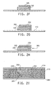
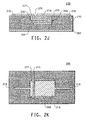
- FIGS. 2A to 2J schematically illustrate steps in manufacturing a second embodiment of a capacitor structure shown in front elevation
- FIG. 2K is a top plan view of the second capacitor structure embodiment.
- FIG. 3 illustrates a third embodiment of a capacitor structure.
- FIGS. 1A-1D illustrate a general method of manufacturing a capacitor structure 100 (FIG. 1 E) having a single-layer capacitor on metallic foil design.
- FIG. 1 E is a plan view of the finished capacitor structure 100. Specific examples of the capacitor structure 100 are also described below.
- FIG. 1A is a side elevational view of first stage of manufacturing the capacitor structure 100.
- a metallic foil 110 is provided.
- the foil 110 may be of a type generally available in the industry.
- the foil 110 may be copper, copper-invar-copper, invar, nickel, nickel-coated copper, or other metals that have melting points in excess of the firing temperature for thick film pastes.
- Preferred foils include foils comprised predominantly of copper, such as reverse treated copper foils, double-treated copper foils, and other copper foils commonly used in the multilayer printed circuit board industry.
- the thickness of the foil 110 may be in the range of, for example, about 1-100 microns, preferably 3-75 microns, and most preferably 12-36 microns, corresponding to between about 1/3 oz and 1 oz copper foil.
- the foil 110 may be pretreated by applying an underprint 112 to the foil 110.
- the underprint 112 is a relatively thin layer applied to a component-side surface of the foil 110.
- the underprint 112 is indicated as a surface coating on the foil 110.
- the underprint 112 adheres well to the metal foil 110 and to layers deposited over the underprint 112.
- the underprint 112 may be formed, for example, from a paste applied to the foil 110, and is then fired at a temperature below the softening point of the foil 110.
- the paste may be printed as an open coating over the entire surface of the foil 110, or printed on selected areas of the foil 110. It is generally more economical to print the underprint paste over selected areas of the foil.
- a dielectric material is screen-printed onto the pretreated foil 110, forming a first dielectric layer 120.
- the dielectric material may be, for example, a thick-film dielectric ink.
- the dielectric ink may be formed of, for example, a paste.
- the first dielectric layer 120 is then dried.
- a second dielectric layer 125 is then applied, and dried.
- a single layer of dielectric material may be deposited through a coarser mesh screen to provide an equivalent thickness in one printing.
- an electrode 130 is formed over the second dielectric layer 125 and dried.
- the electrode 130 can be formed by, for example, screen-printing a thick-film metallic ink.
- the surface area of the dielectric layer 125 should be larger than that of the electrode 130.
- the first dielectric layer 120, the second dielectric layer 125, and the electrode 130 are then co-fired.
- the thick-film dielectric layers 120, 125 may be formed of, for example, a high dielectric constant functional phase such as barium titanate and a dielectric property-modifying additive such as zirconium dioxide, mixed with a glass-ceramic frit phase.
- a high dielectric constant functional phase such as barium titanate
- a dielectric property-modifying additive such as zirconium dioxide
- the glass-ceramic frit phase softens, wets the functional and additive phases and coalesces to create a dispersion of the functional phase and the modifying additive in a glass-ceramic matrix.
- the copper electrode powders of the layer 130 are wetted by the softened glass-ceramic frit phase and sinter together to form a solid electrode.
- the layer 130 has a strong bond to the high K dielectric 128 that results from the co-firing.
- the post-fired structure is shown
- FIG. 1 E is a plan view of the finished capacitor structure 100.
- four dielectric/electrode stacks 140 on the foil 110 are illustrated. Any number of stacks 140, in various patterns, however, can be arranged on a foil 110 to form the capacitor structure 100.
- Examples 1-3 illustrate particular materials and processes used in practicing the general method illustrated by FIGS. 1A-1 E.
- FIGS. 2A-2J illustrate a method of manufacturing a capacitor structure 200 having a double-layer capacitor on metallic foil design.
- FIG. 2K is a plan view of the finished capacitor structure 200.
- FIG. 2A is a front elevational view of first stage of manufacturing the capacitor structure 200.
- a metallic foil 210 is provided.
- the foil 210 may be pretreated by applying and firing an underprint 212, as discussed above with reference to FIG. 1A.
- a dielectric material is screen-printed onto the pretreated foil 210, forming a first dielectric layer 220.
- the first dielectric layer 220 is then dried.
- a second dielectric layer 225 is then applied, and dried.
- a single layer of dielectric material may alternatively be used.
- a first electrode 230 is formed over the second dielectric layer 225 and dried.
- the first electrode may be formed by, for example, screen-printing a thick-film metallic ink.
- the first electrode 230 is formed to extend to contact the foil 210.
- the first dielectric layer 220, the second dielectric layer 225, and the first electrode 230 are then co-fired.
- the dielectric layers 220, 225 may have similar compositions to the materials discussed above with reference to FIGS. 1A-1 E, and the co-firing process imparts the advantages of adhesion and defect-free processing discussed above.
- a resulting dielectric 228 is formed from the co-firing step, as shown in FIG. 2D.
- a third layer of dielectric material is screen-printed onto the co-fired structure of FIG. 2D, forming a third dielectric layer 240.
- the third dielectric layer 240 is then dried.
- a fourth dielectric layer 245 is applied and dried.
- a single layer of dielectric material may alternatively be used.
- FIG. 2G a second electrode 250 is formed over the fourth dielectric layer 245 and dried.
- the second electrode 250 extends to contact the foil 210.
- the structure is then co-fired.
- FIG. 2H illustrates the structure after co-firing, with the resulting dielectric 260 and dielectric/electrode stack 265. After co-firing, the dielectric 260 securely adheres to both electrodes 230, 250, and the electrodes 230, 250 are crack-free.
- a single co-firing can be performed after forming the second electrode 250.
- a single co-firing is advantageous in that production costs are reduced.
- Two separate firings allow inspection of the first electrode 230 for defects such as cracks and for printing alignment issues after the first firing.
- the structure may be inverted and laminated.
- the component face of the foil 210 can be laminated with laminate material 270.
- the lamination can be performed, for example, using FR4 prepreg in standard printing wiring board processes.
- 106 epoxy prepreg may be used.
- Suitable lamination conditions are 185°C at 208 psi for 1 hour in a vacuum chamber evacuated to 28 inches of mercury.
- a silicone rubber press pad and a smooth PTFE filled glass release sheet may be in contact with the foil 210 to prevent the epoxy from gluing the lamination plates together.
- a foil 280 may be applied to the laminate material 270 to provide a surface for creating circuitry.
- the dielectric prepreg and laminate materials can be any type of dielectric material such as, for example, standard epoxy, high Tg epoxy, polyimide, polytetrafluoroethylene, cyanate ester resins, filled resin systems, BT epoxy, and other resins and laminates that provide insulation between circuit layers.
- FIG. 2J after lamination, a photo-resist is applied to the foil 210 and the foil 210 is imaged, etched and stripped using standard printing wiring board processing conditions. The etching produces a trench 215 in the foil 210, which breaks electrical contact between the first electrode 230 and the second electrode 250.
- FIG. 2K is a top plan view of the completed capacitor structure 200.
- a section 216 of the foil 210 is one electrode of the resulting capacitor structure 200, and may be connected to other circuitry by a conductive trace 218.
- a section 227 is coupled to the second electrode 230 and may be connected to other circuitry by a conductive trace 219.
- the capacitor structure 200 discussed above has high capacitance density due to its two-layer capacitor structure.
- the capacitor structure 200 can be produced crack-free by co-firing of the dielectric layers and the electrodes.
- FIG. 3 illustrates a third embodiment of a capacitor structure.
- the capacitor structure 300 is a three-layer embodiment having a high capacitance density.
- the capacitor structure 300 comprises a foil 310 and a plurality of dielectric/electrode stacks 365 (only one stack 365 is illustrated).
- the dielectric/electrode stack 365 include a first electrode 330 and a second electrode 350 separated by a dielectric 360, similar to the first and second electrodes 230, 250 of the capacitor structure 200 discussed above.
- Each dielectric/electrode stack 365 also has a third electrode 335 formed over the dielectric 360.
- a trench 315 breaks electrical contact of a portion 316 of the foil 310 and the electrode 350, from a portion 317 of the foil 310, the first electrode 330, and the third electrode 335.
- a laminate material 370 and a second foil 380 may be included in the capacitor structure 300.
- the capacitor structure 300 can be manufactured in a manner similar to the capacitor structure 200.
- the third layer portion of the dielectrics 360 in the stacks 365 may be formed from one or more dielectric ink layers, as discussed above, and the electrodes 335 can be formed over the dielectrics 360.
- the dielectric/electrode stacks 365 can be co-fired in three individual steps, or in a single step. Firing of each electrode/dielectric layer allows inspection of the product for defects. A single firing, however, reduces the cost of producing the capacitor structure 300.
- the additional layer in the dielectric/electrode stacks 365 provides a high capacitance density for the capacitor structure 300. Co-firing of the dielectric layers and the electrode provides a low dissipation factor and crack-free structure.
- four or more layer capacitor structures can be produced by alternatively forming dielectric and electrode layers, and co-firing the layers.
- the term "paste" may correspond to a conventional term used in the electronic materials industry, and generally refers to a thick-film composition.
- the metal component of the underprint paste is matched to the metal in the metal foil. For example, if a copper foil were used, then a copper paste could be used as the underprint. Examples of other applications would be pairing silver and nickel foils with a similar metal underprint paste. Thick film pastes may be used to form both the underprint and the passive components.
- thick-film pastes comprise finely divided particles of ceramic, glass, metal or other solids dispersed in polymers dissolved in a mixture of plasticizer, dispersing agent and organic solvent.
- Preferred capacitor pastes for use on copper foil have an organic vehicle with good burnout in a nitrogen atmosphere.
- Such vehicles generally contain very small amounts of resin, such as high molecular weight ethyl cellulose, where only small amounts are necessary to generate a viscosity suitable for screen-printing.
- an oxidizing component such as barium nitrate powder, blended into the dielectric powder mixture, helps the organic component burn out in the nitrogen atmosphere.
- Solids are mixed with an essentially inert liquid medium (the "vehicle"), then dispersed on a three-roll mill to form a paste-like composition suitable for screen-printing.
- essentially inert liquid may be used as the vehicle.
- various organic liquids, with or without thickening and/or stabilizing agents and/or other common additives, may be used as the vehicle.
- High K thick-film dielectric pastes generally contain at least one high K functional phase powder and at least one glass powder dispersed in a vehicle system composed of at least one resin and a solvent.
- the vehicle system is designed to be screen-printed to provide a dense and spatially well-defined film.
- the high K functional phase powders can comprise perovskite-type ferroelectric compositions with the general formula ABO 3 . Examples of such compositions include BaTiO 3 ; SrTiO 3 ; PbTiO 3 ; CaTiO 3 ; PbZrO 3 ; BaZrO 3 and SrZrO 3 .
- compositions are also possible by substitution of alternative elements into the A and/or B position, such as Pb(Mg 1/3 Nb 2/3 )O 3 and Pb(Zn 1/3 Nb 2/3 )O 3 .
- Pb(Mg 1/3 Nb 2/3 )O 3 and Pb(Zn 1/3 Nb 2/3 )O 3 are other possible high K materials.
- Doped and mixed metal versions of the above compositions are also suitable. Doping and mixing is done primarily to achieve the necessary end-use property specifications such as, for example, the necessary temperature coefficient of capacitance (TCC) in order for the material to meet industry definitions, such as "X7R” or "Z5U” standards.
- TCC temperature coefficient of capacitance
- the glasses in the pastes can be, for example, Ca-Al borosilicates, Pb-Ba borosilicates, Mg-AI silicates, rare earth borates, and other similar glass compositions.
- Pastes used to form the electrode layers may be based on metallic powders of either copper, nickel, silver, silver-containing precious metal compositions, or mixtures of these compounds. Copper powder compositions are preferred.
- capacitor structure embodiments described in this specification have many applications.
- the capacitor structure embodiments can be used within organic printed circuit boards, IC packages, applications of said structures in decoupling applications, and devices such as IC modules or handheld device motherboards.
- the electrode layers are described as formed by screen-printing. Other methods, however, such as deposition by sputtering or evaporation of electrode metals onto the dielectric layer surface may also be used.
- the foil 110 was a copper foil.
- the type of copper foil 110 can be any commercial grade of copper foil used in the printed wiring board industry, and may be in the range of 1/3 oz copper foil (approximately 12 microns thickness) to 1 oz copper foil (approximately 36 microns thickness).
- the copper foil 110 was pretreated by applying a copper underprint paste over selected areas of the foil 110. The resulting product was then fired in nitrogen at 900°C for 10 minutes at peak temperature, with a total cycle time of approximately 1 hour, forming the underprint 112.
- a thick-film dielectric ink was screen-printed onto the pretreated copper foil 110 through 400 mesh screen to create a pattern of 1 ⁇ 2 inch by 1 ⁇ 2 inch first dielectric layers 120.
- the wet printed thickness of the first dielectric layers 120 is approximately 12-15 microns.
- the first dielectric layers 120 were dried at 125°C for approximately 10 minutes, and second dielectric layers 125 were applied by screen-printing, followed by another drying step at 125°C.
- the thick-film dielectric ink included a barium titanate component, a zirconium oxide component, and a glass-ceramic phase.
- thick-film copper electrode ink layers 130 was printed through 400 mesh screens onto the dielectric squares 120, and dried at 125°C for approximately 10 minutes to form a 0.9 cm by 0.9 cm square electrode.
- the printed electrode 130 thickness was limited only by the need for a pinhole-free film, and was typically in the range of 3 to 15 microns.
- the resulting structure was co-fired to 900°C for 10 minutes at peak temperature using a thick film nitrogen profile.
- the nitrogen profile included less than 50 ppm oxygen in the burnout zone, and 2-10 ppm oxygen in the firing zone, with a total cycle time of 1 hour.
- Co-firing resulted in the dielectric/electrode stacks 140 illustrated in FIG. 1 E.
- the thick film dielectric material had the following composition: Barium titanate powder 64.18% Zirconium oxide powder 3.78 % Glass A 11.63 % Ethyl cellulose 0.86 % Texanol 18.21 % Barium nitrate powder 0.84 % Phosphate wetting agent 0.5 %. Glass A comprised: Germanium oxide 21.5 % Lead tetraoxide 78.5 %.
- the Glass A composition corresponded to Pb 5 Ge 3 O 11 , which precipitated out during the firing, and had a dielectric constant of approximately 70-150.
- the thick film copper electrode ink comprised: Copper powder 55.1 % Glass A 1.6 % Cuprous oxide powder 5.6 % Ethyl cellulose T-200 1.7 % Texanol 36.0 %.
- the capacitor structure was crack free and had the following electrical characteristics: capacitance density approximately 150 nF/in 2 dissipation factor approximately 1.5 % insulation resistance > 5 x 10 9 Ohms breakdown voltage approximately 800 volts/mil.
- the use of copper as the material to form the foil 110 and the electrodes 130 was advantageous because copper was not subject to a large degree of migration.
- the large TCE difference between copper and dielectric materials leads to cracking and separation of the electrode from the dielectric, and high dissipation factors.
- cracking did not occur and low dissipation factors were achieved.
- Example 2 A process as described in Example 1 was repeated, except that the thick-film dielectric 128 was printed through 325 mesh screen, with a wet thickness of each of the two layers of approximately 15-20 microns. Results were similar to the embodiment of Example 1, except that the capacitance density was approximately 120 nF/inch 2 .
- Example 2 A process as described in Example 2 was repeated using a variety of dielectric and electrode dimensions shown in the table below: Dielectric Size mils Electrode Size mils Dielectric Size mils Electrode Size mils 250 x 250 210 x 210 36 x 338 20 x 320 56 x 340 40 x 320 96 x 340 80 x 320 176 x 340 160 x 320 36 x 178 20 x 157 96 x 180 80 x 158 336 x 180 320 x 158 26 x 180 10 x 159 56 x 180 40 x 158 176 x 180 160 x 158 26 x 100 10 x 74 36 x 98 20 x 77 56 x 100 40 x 78 56 x 100 40 x 78 96 x 100 80 x 78 176x100 160x78 26x60 10x39 36x58 20x37 56x60 40x38 96x60 80x38 26x40 10x18 36x38 16x17 56 x 40 40
- Capacitance in these embodiments was proportional to the area of the printed copper electrode, but the calculated capacitance densities were essentially identical to that of Example 1.
Landscapes
- Engineering & Computer Science (AREA)
- Power Engineering (AREA)
- Microelectronics & Electronic Packaging (AREA)
- Manufacturing & Machinery (AREA)
- Chemical & Material Sciences (AREA)
- Ceramic Engineering (AREA)
- Inorganic Chemistry (AREA)
- Fixed Capacitors And Capacitor Manufacturing Machines (AREA)
- Ceramic Capacitors (AREA)
- Parts Printed On Printed Circuit Boards (AREA)
Applications Claiming Priority (2)
| Application Number | Priority Date | Filing Date | Title |
|---|---|---|---|
| US41804502P | 2002-10-11 | 2002-10-11 | |
| US418045P | 2002-10-11 |
Publications (3)
| Publication Number | Publication Date |
|---|---|
| EP1408520A2 true EP1408520A2 (de) | 2004-04-14 |
| EP1408520A3 EP1408520A3 (de) | 2005-02-09 |
| EP1408520B1 EP1408520B1 (de) | 2008-12-10 |
Family
ID=32030982
Family Applications (1)
| Application Number | Title | Priority Date | Filing Date |
|---|---|---|---|
| EP03022085A Expired - Lifetime EP1408520B1 (de) | 2002-10-11 | 2003-10-02 | Zusammengesinterter Keramik-Kondensator und Verfahren zur Herstellung von Keramik-Kondensatoren für gedruckte Schaltungen |
Country Status (7)
| Country | Link |
|---|---|
| US (2) | US20040099999A1 (de) |
| EP (1) | EP1408520B1 (de) |
| JP (2) | JP2004134806A (de) |
| KR (1) | KR100553635B1 (de) |
| CN (1) | CN100477030C (de) |
| DE (1) | DE60325156D1 (de) |
| TW (1) | TWI277375B (de) |
Cited By (3)
| Publication number | Priority date | Publication date | Assignee | Title |
|---|---|---|---|---|
| EP1677320A1 (de) * | 2004-12-28 | 2006-07-05 | E.I.Du pont de nemours and company | Brennen von Bariumtitanat auf Kupferfolie unter Sauerstoffdotierung |
| EP1737283A1 (de) * | 2005-06-20 | 2006-12-27 | E.I.Du pont de nemours and company | Eingebettete Kondensatoren, elektronische Vorrichtungen mit solchen Kondensatoren und Verfahren zur Herstellung derselben |
| US7750248B2 (en) | 2005-12-07 | 2010-07-06 | Ngk Spark Plug Co., Ltd. | Dielectric lamination structure, manufacturing method of a dielectric lamination structure, and wiring board including a dielectric lamination structure |
Families Citing this family (46)
| Publication number | Priority date | Publication date | Assignee | Title |
|---|---|---|---|---|
| US20040231885A1 (en) * | 2003-03-07 | 2004-11-25 | Borland William J. | Printed wiring boards having capacitors and methods of making thereof |
| US8569142B2 (en) * | 2003-11-28 | 2013-10-29 | Blackberry Limited | Multi-level thin film capacitor on a ceramic substrate and method of manufacturing the same |
| JP4700332B2 (ja) | 2003-12-05 | 2011-06-15 | イビデン株式会社 | 多層プリント配線板 |
| US6908809B1 (en) * | 2004-04-02 | 2005-06-21 | Harris Corporation | Embedded capacitors using conductor filled vias |
| US20060000542A1 (en) * | 2004-06-30 | 2006-01-05 | Yongki Min | Metal oxide ceramic thin film on base metal electrode |
| US7100277B2 (en) * | 2004-07-01 | 2006-09-05 | E. I. Du Pont De Nemours And Company | Methods of forming printed circuit boards having embedded thick film capacitors |
| US7290315B2 (en) * | 2004-10-21 | 2007-11-06 | Intel Corporation | Method for making a passive device structure |
| US20060099803A1 (en) * | 2004-10-26 | 2006-05-11 | Yongki Min | Thin film capacitor |
| US20060091495A1 (en) * | 2004-10-29 | 2006-05-04 | Palanduz Cengiz A | Ceramic thin film on base metal electrode |
| US20060120015A1 (en) | 2004-12-02 | 2006-06-08 | Borland William J | Thick-film capacitors, embedding thick-film capacitors inside printed circuit boards, and methods of forming such capacitors and printed circuit boards |
| JP4584700B2 (ja) * | 2004-12-17 | 2010-11-24 | 新光電気工業株式会社 | 配線基板の製造方法 |
| US20060158828A1 (en) * | 2004-12-21 | 2006-07-20 | Amey Daniel I Jr | Power core devices and methods of making thereof |
| US7613007B2 (en) * | 2004-12-21 | 2009-11-03 | E. I. Du Pont De Nemours And Company | Power core devices |
| JP4667070B2 (ja) * | 2005-02-23 | 2011-04-06 | 日本特殊陶業株式会社 | 配線基板及び配線基板の製造方法 |
| US20060220177A1 (en) * | 2005-03-31 | 2006-10-05 | Palanduz Cengiz A | Reduced porosity high-k thin film mixed grains for thin film capacitor applications |
| US7375412B1 (en) | 2005-03-31 | 2008-05-20 | Intel Corporation | iTFC with optimized C(T) |
| US7629269B2 (en) * | 2005-03-31 | 2009-12-08 | Intel Corporation | High-k thin film grain size control |
| US20060282999A1 (en) * | 2005-06-20 | 2006-12-21 | Diptarka Majumdar | Electrodes, inner layers, capacitors and printed wiring boards and methods of making thereof - part II |
| US7453144B2 (en) | 2005-06-29 | 2008-11-18 | Intel Corporation | Thin film capacitors and methods of making the same |
| US7621041B2 (en) * | 2005-07-11 | 2009-11-24 | E. I. Du Pont De Nemours And Company | Methods for forming multilayer structures |
| US7456459B2 (en) * | 2005-10-21 | 2008-11-25 | Georgia Tech Research Corporation | Design of low inductance embedded capacitor layer connections |
| US7705423B2 (en) * | 2005-10-21 | 2010-04-27 | Georgia Tech Research Corporation | Device having an array of embedded capacitors for power delivery and decoupling of high speed input/output circuitry of an integrated circuit |
| US7504706B2 (en) * | 2005-10-21 | 2009-03-17 | E. I. Du Pont De Nemours | Packaging having an array of embedded capacitors for power delivery and decoupling in the mid-frequency range and methods of forming thereof |
| EP1777745A3 (de) * | 2005-10-21 | 2010-05-05 | E.I. Du Pont De Nemours And Company | Versorgungvorrichtung mit Kondensator und deren Herstellungsverfahren |
| JP5006613B2 (ja) * | 2006-02-09 | 2012-08-22 | 日本特殊陶業株式会社 | 多層配線基板内蔵用コンデンサ及びそのコンデンサを内蔵した多層配線基板 |
| JP4758235B2 (ja) * | 2006-01-23 | 2011-08-24 | 日本特殊陶業株式会社 | 誘電体積層構造体の製造方法 |
| JP2007242838A (ja) * | 2006-03-08 | 2007-09-20 | Tdk Corp | コンデンサの製造方法 |
| US20080010798A1 (en) * | 2006-07-14 | 2008-01-17 | Borland William J | Thin film dielectrics with co-fired electrodes for capacitors and methods of making thereof |
| US7818855B2 (en) * | 2006-11-10 | 2010-10-26 | E. I. Du Pont De Nemours And Company | Method of making thin-film capacitors on metal foil using thick top electrodes |
| US7685687B2 (en) | 2007-01-22 | 2010-03-30 | E. I. Du Pont De Nemours And Company | Methods of making high capacitance density ceramic capacitors |
| US8059423B2 (en) * | 2007-02-06 | 2011-11-15 | Sanmina-Sci Corporation | Enhanced localized distributive capacitance for circuit boards |
| US20090168391A1 (en) * | 2007-12-27 | 2009-07-02 | Kouichi Saitou | Substrate for mounting device and method for producing the same, semiconductor module and method for producing the same, and portable apparatus provided with the same |
| KR101420147B1 (ko) * | 2009-03-31 | 2014-07-21 | 주식회사 잉크테크 | 박막 캐패시터의 제조 방법 |
| KR101172709B1 (ko) | 2009-06-24 | 2012-08-09 | 주식회사 이그잭스 | 엘이디 어레이 기판 및 이의 제조방법 |
| JP2013127992A (ja) * | 2010-03-26 | 2013-06-27 | Sanyo Electric Co Ltd | コンデンサ内蔵基板の製造方法、及び該製造方法に使用可能な素子シートの製造方法 |
| WO2012014648A1 (ja) * | 2010-07-30 | 2012-02-02 | 三洋電機株式会社 | 基板内蔵用キャパシタ、これを備えたキャパシタ内蔵基板、及び基板内蔵用キャパシタの製造方法 |
| JPWO2012014647A1 (ja) * | 2010-07-30 | 2013-09-12 | 三洋電機株式会社 | 基板内蔵用キャパシタ、これを備えたキャパシタ内蔵基板、及び基板内蔵用キャパシタの製造方法 |
| DE102012217168A1 (de) * | 2012-09-24 | 2014-04-17 | Siemens Aktiengesellschaft | Verfahren zum Herstellen eines Kondensators und Kondensator |
| US20170022112A1 (en) * | 2015-07-21 | 2017-01-26 | Quantumscape Corporation | Processes and materials for casting and sintering green garnet thin films |
| US9881747B2 (en) * | 2016-01-29 | 2018-01-30 | The United States Of America As Represented By The Administrator Of The National Aeronautics And Space Administration | Solid state ultracapacitor |
| JP2018063989A (ja) | 2016-10-11 | 2018-04-19 | Tdk株式会社 | 薄膜キャパシタ |
| JP6737118B2 (ja) | 2016-10-11 | 2020-08-05 | Tdk株式会社 | 薄膜コンデンサ |
| JP6805702B2 (ja) | 2016-10-11 | 2020-12-23 | Tdk株式会社 | 薄膜コンデンサ |
| DE102017200503B4 (de) | 2017-01-13 | 2023-02-16 | Fraunhofer-Gesellschaft zur Förderung der angewandten Forschung e.V. | Verfahren zur Herstellung eines dielektrischen Elements |
| US10330813B2 (en) * | 2017-07-11 | 2019-06-25 | Joyson Safety Systems Acquisition Llc | Occupant detection system |
| CN109888308A (zh) * | 2019-04-09 | 2019-06-14 | 深圳市致远动力科技有限公司 | 一种以电解质层为基体的燃料电池及其制备方法 |
Family Cites Families (31)
| Publication number | Priority date | Publication date | Assignee | Title |
|---|---|---|---|---|
| US179329A (en) * | 1876-06-27 | Improvement in combined portmanteaus and shawl-straps | ||
| US154592A (en) * | 1874-09-01 | Improvement in wooden shoes | ||
| US4063341A (en) * | 1975-07-09 | 1977-12-20 | E. I. Du Pont De Nemours And Company | Process for making multilayer capacitors |
| US4066426A (en) * | 1976-05-26 | 1978-01-03 | Sprague Electric Company | Method of forming a glass-reacted-ceramic with cadmium |
| US4190854A (en) * | 1978-02-15 | 1980-02-26 | National Semiconductor Corporation | Trim structure for integrated capacitors |
| US4528613A (en) * | 1984-02-24 | 1985-07-09 | Trw Inc. | Ceramic glass material, capacitor made therefrom and method of making the same |
| US4526613A (en) | 1984-03-12 | 1985-07-02 | Union Carbide Corporation | Production of alloy steels using chemically prepared V2 O3 as a vanadium additive |
| US4533974A (en) * | 1984-04-09 | 1985-08-06 | Sprague Electric Company | Low-firing high Q monolithic ceramic capacitor |
| US4906405A (en) * | 1987-05-19 | 1990-03-06 | Matsushita Electric Industrial Co., Ltd. | Conductor composition and method of manufacturing a multilayered ceramic body using the composition |
| US5208597A (en) * | 1988-10-13 | 1993-05-04 | Crystal Semiconductor | Compensated capacitors for switched capacitor input of an analog-to-digital converter |
| JPH0614580B2 (ja) | 1988-11-04 | 1994-02-23 | イビデン株式会社 | 厚膜素子を有するプリント配線板およびその製造方法 |
| JPH02153589A (ja) | 1988-12-05 | 1990-06-13 | Ibiden Co Ltd | 厚膜素子付プリント配線板 |
| US5256469A (en) * | 1991-12-18 | 1993-10-26 | General Electric Company | Multi-layered, co-fired, ceramic-on-metal circuit board for microelectronic packaging |
| US5362534A (en) * | 1993-08-23 | 1994-11-08 | Parlex Corporation | Multiple layer printed circuit boards and method of manufacture |
| US5509200A (en) * | 1994-11-21 | 1996-04-23 | International Business Machines Corporation | Method of making laminar stackable circuit board structure |
| JPH08279669A (ja) | 1995-04-07 | 1996-10-22 | Hokuriku Electric Ind Co Ltd | コンデンサ付き回路基板の製造方法 |
| US6631551B1 (en) * | 1998-06-26 | 2003-10-14 | Delphi Technologies, Inc. | Method of forming integral passive electrical components on organic circuit board substrates |
| US6215649B1 (en) * | 1998-11-05 | 2001-04-10 | International Business Machines Corporation | Printed circuit board capacitor structure and method |
| KR20000034924A (ko) | 1998-11-17 | 2000-06-26 | 제닌 엠. 데이비스 | 저온 동시소성 다층세라믹내 수동 전자소자들 |
| US6274224B1 (en) | 1999-02-01 | 2001-08-14 | 3M Innovative Properties Company | Passive electrical article, circuit articles thereof, and circuit articles comprising a passive electrical article |
| US6252761B1 (en) * | 1999-09-15 | 2001-06-26 | National Semiconductor Corporation | Embedded multi-layer ceramic capacitor in a low-temperature con-fired ceramic (LTCC) substrate |
| US6317023B1 (en) * | 1999-10-15 | 2001-11-13 | E. I. Du Pont De Nemours And Company | Method to embed passive components |
| US6525921B1 (en) * | 1999-11-12 | 2003-02-25 | Matsushita Electric Industrial Co., Ltd | Capacitor-mounted metal foil and a method for producing the same, and a circuit board and a method for producing the same |
| US6370013B1 (en) * | 1999-11-30 | 2002-04-09 | Kyocera Corporation | Electric element incorporating wiring board |
| JP3964085B2 (ja) | 1999-12-09 | 2007-08-22 | 大日本印刷株式会社 | プリント配線基板、及びプリント配線基板の製造方法 |
| DE10042653A1 (de) * | 2000-08-31 | 2002-03-28 | Bosch Gmbh Robert | Keramische Mehrlagenschaltung |
| JP4613416B2 (ja) * | 2000-11-28 | 2011-01-19 | 日本電気株式会社 | 半導体装置およびその実装方法 |
| US6426250B1 (en) * | 2001-05-24 | 2002-07-30 | Taiwan Semiconductor Manufacturing Company | High density stacked MIM capacitor structure |
| EP1265466A3 (de) * | 2001-06-05 | 2004-07-21 | Dai Nippon Printing Co., Ltd. | Verfahren zur Herstellung einer Leiterplatte mit passiven Elementen und Leiterplatte mit passiven Elementen |
| JP3946578B2 (ja) | 2001-06-05 | 2007-07-18 | 大日本印刷株式会社 | 受動素子を備えた配線板の製造方法、受動素子を備えた配線板 |
| US6860000B2 (en) * | 2002-02-15 | 2005-03-01 | E.I. Du Pont De Nemours And Company | Method to embed thick film components |
-
2003
- 2003-08-29 US US10/651,367 patent/US20040099999A1/en not_active Abandoned
- 2003-09-19 TW TW092125943A patent/TWI277375B/zh not_active IP Right Cessation
- 2003-10-02 DE DE60325156T patent/DE60325156D1/de not_active Expired - Lifetime
- 2003-10-02 EP EP03022085A patent/EP1408520B1/de not_active Expired - Lifetime
- 2003-10-10 KR KR1020030070509A patent/KR100553635B1/ko not_active Expired - Fee Related
- 2003-10-13 CN CNB2003101006793A patent/CN100477030C/zh not_active Expired - Fee Related
- 2003-10-14 JP JP2003354152A patent/JP2004134806A/ja active Pending
-
2004
- 2004-06-28 US US10/878,877 patent/US7072167B2/en not_active Expired - Lifetime
-
2005
- 2005-10-18 JP JP2005303285A patent/JP2006086538A/ja active Pending
Cited By (4)
| Publication number | Priority date | Publication date | Assignee | Title |
|---|---|---|---|---|
| EP1677320A1 (de) * | 2004-12-28 | 2006-07-05 | E.I.Du pont de nemours and company | Brennen von Bariumtitanat auf Kupferfolie unter Sauerstoffdotierung |
| EP1737283A1 (de) * | 2005-06-20 | 2006-12-27 | E.I.Du pont de nemours and company | Eingebettete Kondensatoren, elektronische Vorrichtungen mit solchen Kondensatoren und Verfahren zur Herstellung derselben |
| US7750248B2 (en) | 2005-12-07 | 2010-07-06 | Ngk Spark Plug Co., Ltd. | Dielectric lamination structure, manufacturing method of a dielectric lamination structure, and wiring board including a dielectric lamination structure |
| US8813353B2 (en) | 2005-12-07 | 2014-08-26 | Ngk Spark Plug Co., Ltd. | Method of manufacturing a dielectric structure |
Also Published As
| Publication number | Publication date |
|---|---|
| TW200410608A (en) | 2004-06-16 |
| US7072167B2 (en) | 2006-07-04 |
| CN100477030C (zh) | 2009-04-08 |
| DE60325156D1 (de) | 2009-01-22 |
| TWI277375B (en) | 2007-03-21 |
| US20040099999A1 (en) | 2004-05-27 |
| JP2004134806A (ja) | 2004-04-30 |
| KR20040033262A (ko) | 2004-04-21 |
| US20040233611A1 (en) | 2004-11-25 |
| JP2006086538A (ja) | 2006-03-30 |
| CN1497627A (zh) | 2004-05-19 |
| EP1408520A3 (de) | 2005-02-09 |
| EP1408520B1 (de) | 2008-12-10 |
| KR100553635B1 (ko) | 2006-02-20 |
Similar Documents
| Publication | Publication Date | Title |
|---|---|---|
| US7072167B2 (en) | Co-fired ceramic capacitor and method for forming ceramic capacitors for use in printed wiring boards | |
| KR100562812B1 (ko) | 커패시터를 갖는 인쇄 배선 기판 및 그 제조 방법 | |
| US7100277B2 (en) | Methods of forming printed circuit boards having embedded thick film capacitors | |
| KR101046890B1 (ko) | 다층 프린트 배선판 | |
| KR100584803B1 (ko) | 고내성 내장 커패시터 | |
| US20040108134A1 (en) | Printed wiring boards having low inductance embedded capacitors and methods of making same | |
| US20070220725A1 (en) | Thick-film capacitors, embedding thick-film capacitors inside printed circuit boards, and methods of forming such capacitors and printed circuit boards | |
| JP2006179923A (ja) | 電力コアデバイス、およびその作製の方法 | |
| KR100713731B1 (ko) | 낮은 인덕턴스의 내장 커패시터를 구비한 인쇄 배선 기판및 그 제조 방법 | |
| KR20090023696A (ko) | 개선된 전극, 내부층, 커패시터 및 인쇄 배선 기판, 및 이들의 제조 방법- 파트 ⅱ | |
| JP2007116177A (ja) | 電力コアデバイスおよびその製造方法 | |
| US7741189B2 (en) | Electrodes, inner layers, capacitors, electronic devices and methods of making thereof | |
| JP2005129887A (ja) | コンデンサを有する印刷配線板とその製造方法 | |
| HK1064798A (en) | Co-fired ceramic capacitor and method for forming ceramic capacitors for use in printed wiring boards |
Legal Events
| Date | Code | Title | Description |
|---|---|---|---|
| PUAI | Public reference made under article 153(3) epc to a published international application that has entered the european phase |
Free format text: ORIGINAL CODE: 0009012 |
|
| AK | Designated contracting states |
Kind code of ref document: A2 Designated state(s): AT BE BG CH CY CZ DE DK EE ES FI FR GB GR HU IE IT LI LU MC NL PT RO SE SI SK TR |
|
| AX | Request for extension of the european patent |
Extension state: AL LT LV MK |
|
| PUAL | Search report despatched |
Free format text: ORIGINAL CODE: 0009013 |
|
| AK | Designated contracting states |
Kind code of ref document: A3 Designated state(s): AT BE BG CH CY CZ DE DK EE ES FI FR GB GR HU IE IT LI LU MC NL PT RO SE SI SK TR |
|
| AX | Request for extension of the european patent |
Extension state: AL LT LV MK |
|
| RIC1 | Information provided on ipc code assigned before grant |
Ipc: 7H 01G 9/04 B Ipc: 7H 01G 4/33 B Ipc: 7H 01G 4/30 A |
|
| 17P | Request for examination filed |
Effective date: 20050415 |
|
| AKX | Designation fees paid |
Designated state(s): DE FR GB |
|
| 17Q | First examination report despatched |
Effective date: 20050905 |
|
| GRAP | Despatch of communication of intention to grant a patent |
Free format text: ORIGINAL CODE: EPIDOSNIGR1 |
|
| GRAS | Grant fee paid |
Free format text: ORIGINAL CODE: EPIDOSNIGR3 |
|
| GRAA | (expected) grant |
Free format text: ORIGINAL CODE: 0009210 |
|
| AK | Designated contracting states |
Kind code of ref document: B1 Designated state(s): DE FR GB |
|
| REG | Reference to a national code |
Ref country code: GB Ref legal event code: FG4D |
|
| REF | Corresponds to: |
Ref document number: 60325156 Country of ref document: DE Date of ref document: 20090122 Kind code of ref document: P |
|
| PLBE | No opposition filed within time limit |
Free format text: ORIGINAL CODE: 0009261 |
|
| STAA | Information on the status of an ep patent application or granted ep patent |
Free format text: STATUS: NO OPPOSITION FILED WITHIN TIME LIMIT |
|
| 26N | No opposition filed |
Effective date: 20090911 |
|
| PGFP | Annual fee paid to national office [announced via postgrant information from national office to epo] |
Ref country code: GB Payment date: 20090930 Year of fee payment: 7 |
|
| PGFP | Annual fee paid to national office [announced via postgrant information from national office to epo] |
Ref country code: DE Payment date: 20090923 Year of fee payment: 7 |
|
| PGFP | Annual fee paid to national office [announced via postgrant information from national office to epo] |
Ref country code: FR Payment date: 20091029 Year of fee payment: 7 |
|
| GBPC | Gb: european patent ceased through non-payment of renewal fee |
Effective date: 20101002 |
|
| PG25 | Lapsed in a contracting state [announced via postgrant information from national office to epo] |
Ref country code: FR Free format text: LAPSE BECAUSE OF NON-PAYMENT OF DUE FEES Effective date: 20101102 |
|
| REG | Reference to a national code |
Ref country code: FR Ref legal event code: ST Effective date: 20110630 |
|
| PG25 | Lapsed in a contracting state [announced via postgrant information from national office to epo] |
Ref country code: GB Free format text: LAPSE BECAUSE OF NON-PAYMENT OF DUE FEES Effective date: 20101002 |
|
| REG | Reference to a national code |
Ref country code: DE Ref legal event code: R119 Ref document number: 60325156 Country of ref document: DE Effective date: 20110502 |
|
| PG25 | Lapsed in a contracting state [announced via postgrant information from national office to epo] |
Ref country code: DE Free format text: LAPSE BECAUSE OF NON-PAYMENT OF DUE FEES Effective date: 20110502 |