EP1408727A2 - Steckkarte zur elektronischen Datenverarbeitung - Google Patents
Steckkarte zur elektronischen Datenverarbeitung Download PDFInfo
- Publication number
- EP1408727A2 EP1408727A2 EP03020037A EP03020037A EP1408727A2 EP 1408727 A2 EP1408727 A2 EP 1408727A2 EP 03020037 A EP03020037 A EP 03020037A EP 03020037 A EP03020037 A EP 03020037A EP 1408727 A2 EP1408727 A2 EP 1408727A2
- Authority
- EP
- European Patent Office
- Prior art keywords
- latching
- plug
- card according
- longitudinal
- longitudinal side
- Prior art date
- Legal status (The legal status is an assumption and is not a legal conclusion. Google has not performed a legal analysis and makes no representation as to the accuracy of the status listed.)
- Granted
Links
- 238000012216 screening Methods 0.000 description 8
- 238000000034 method Methods 0.000 description 4
- 230000001154 acute effect Effects 0.000 description 3
- 238000011161 development Methods 0.000 description 3
- 230000018109 developmental process Effects 0.000 description 3
- 238000006073 displacement reaction Methods 0.000 description 3
- 238000005452 bending Methods 0.000 description 2
- 210000005069 ears Anatomy 0.000 description 2
- 238000004519 manufacturing process Methods 0.000 description 2
- 230000005489 elastic deformation Effects 0.000 description 1
- 238000005304 joining Methods 0.000 description 1
- 239000002184 metal Substances 0.000 description 1
- 238000003825 pressing Methods 0.000 description 1
- 230000000284 resting effect Effects 0.000 description 1
Images




Classifications
-
- H—ELECTRICITY
- H05—ELECTRIC TECHNIQUES NOT OTHERWISE PROVIDED FOR
- H05K—PRINTED CIRCUITS; CASINGS OR CONSTRUCTIONAL DETAILS OF ELECTRIC APPARATUS; MANUFACTURE OF ASSEMBLAGES OF ELECTRICAL COMPONENTS
- H05K5/00—Casings, cabinets or drawers for electric apparatus
- H05K5/02—Details
- H05K5/0256—Details of interchangeable modules or receptacles therefor, e.g. cartridge mechanisms
- H05K5/026—Details of interchangeable modules or receptacles therefor, e.g. cartridge mechanisms having standardized interfaces
- H05K5/0265—Details of interchangeable modules or receptacles therefor, e.g. cartridge mechanisms having standardized interfaces of PCMCIA type
- H05K5/0269—Card housings therefor, e.g. covers, frames, PCB
Definitions
- the present invention relates to a plug-in card for electronic data-processing devices according to the preamble of Claim 1.
- the two metallic half-shells are symmetrically constructed in such a way that the longitudinal walls reach around one another to latch over their entire length. This has advantages in terms of manufacturing technique and results in a good screening of the components disposed inside. However, it has emerged that, because the housing half-shells must first be twisted in order to interlock or to reach around, assembly is not without its problems.
- the problem addressed by the present invention is therefore to provide a plug-in card for electronic data-processing devices of the kind mentioned above, the housing portions of which are simplified in terms of assembly technique without impairing the screening of the electronic components disposed inside.
- Claim 1 the features specified in Claim 1 are provided for a plug-in card for electronic data-processing devices of the kind mentioned.
- a simplified assembly of the two housing portions is achieved by the measures according to the invention in such a way that the said portions, in plane disposition and displaced in perpendicular one upon the other, may be joined to latch with one another by simple plugging. Optimum screening continues to be provided.
- the latching recesses are provided directly in the longitudinal sidewall, according to the features of Claim 2.
- the free edge may conveniently rest by its middle region on the edge of the latching recess or latching slot, while the side regions of the latching edge reach behind the latching slots over the inside surface of the one longitudinal side wall.
- the features according to Claim 14 contribute advantageously to the optimum screening of the electronic components arranged, for example, on a printed circuit board inside the housing, because unscreened gaps are avoided.
- the two half-shell-type housing portions are simplified in terms of manufacturing technique, but likewise offer advantages in terms of assembly technique.
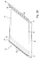
- the unframed plug-in card 10 (according to Figures 2 to 5) and 110 (according to Figures 9 and 10) for electronic data-processing devices, represented in assembled state in Figure 1 but without showing a male connector, has an oblong rectangular and very flat housing 11 which is comprised of a bottom housing portion 12 and a top housing portion 13 joined to the latter by latching.
- a unit disposed and held fixed between the two housing portions 12 and 13, in a manner not shown, has a printed circuit board populated with electronic components and a plug-in connector respectively disposed at one transverse end of and connected to the printed circuit board.
- Both housing portions 12 and 13 are stamped from thin sheet metal and formed to be like half shells.
- the housing portion 12 and 13 are constructed identically.
- the housing portion 12 and 13 respectively has a base 21 which is formed to project outwards at a large-surfaced central region 22. Both longitudinal edges 23 and 24 pass into an L-shaped longitudinal wall 27 and 28 respectively.
- the two legs 31 of the longitudinal wall 27 and respectively 28 perpendicular to the base 21 are the same in length, while the transverse legs 33 and respectively 34 extending parallel to the base 21 are of different length.
- Studs 17 bent at right angles are arranged at one plane end region 16 of the two housing portions 12 and 13, disposed within the longitudinal edges 22, 24 and overlapping one another in plugged-together state and accommodating and holding between them the male connector which is not shown.
- the L-shaped longitudinal wall 28 of both housing portions 12 and 13 having the wide transverse leg 34 is provided with rectangular slots 36 disposed one after the other at equal spacing in the longitudinal direction.
- the narrow transverse leg 33 of the L-shaped longitudinal wall 27 of the two housing portions 12 and 13 is adjoined by latching lugs 37 which are likewise disposed one after the other at certain uniform spacings in the longitudinal direction.
- the slots 36 on one longitudinal edge 24 and the latching lugs 37 on the other longitudinal edge 27 are disposed and provided at the same spacings and in the same numbers and in substantially the same widths.
- the latching lugs 37 fit into and through the slots 36, so that a latching connection of the housing portions 12 and 13 as represented in Figure 5 may be effected at both longitudinal edges 23 and 24 of the plug-in card 10.
- the latching lugs 37 adjoin the narrow transverse leg 33 and are bent down in a direction facing away from the base 21 to extend inward at a slight acute angle to the longitudinal leg 31 ( Figures 3 and 4).
- the latching lugs 37 have a main portion 38 which adjoins the transverse leg 33 and is provided in one piece at its other end with a latching portion 39 which is bent back.
- Approximately V-shaped latching lugs 37 comprising a latching portion 39 and a main portion 38 are produced in this manner.
- the V-shape of the latching lug 37 is such that the latching lug 37 when pushed through the latching slot 36 can compress elastically together in the direction of the Arrow B when being pushed through, and can expand once again after the free edge 42 of the latching portion 29 has left the latching slot 36.
- the spacing between the free edge 42 and the fold 43 joining the main portion 38 and the latching portion 39 is at least equal to and preferably smaller than the inside width 44 of the U-shaped longitudinal edge 24.
- the free end of the latching portion 39 is shaped in the region of its free edge 42 in such a way that a slightly groove-like edge 42 is produced and that ears 47 are slightly bent down from both ends of a central region 46 towards the main portion 38. This means that, in the latched state, the ears 47 rest substantially on the inner side of the transverse leg 34.
- the latching lugs 37 are shaped slightly conically along their end face 48, in a manner not shown in detail, in order to form a chamfer for introduction into the slots 36.
- the latching lugs 37 held inside the U-shaped longitudinal edge 24 in the latched state are encompassed in an approximately L-shaped manner by a preferably one-piece plastic retaining strip 51 extending over the entire length of the housing portions 12, 13.
- the longitudinal leg of the L-shaped retaining strip 51 resting on the latching portion 38 has a slightly conical inner wall to correspond to the extension of the latching portion 39.
- the transverse leg of the L-shaped retaining strip 51 is relatively thin and rests on the fold 43 of the locating lug 37 and substantially fills out the spacing between the fold 43 and the inner surface of the base 21.
- the retaining strip 51 which is inserted at the respective longitudinal edge 24 before the two housing portions 12 and 13 are latched to form the housing, is held fixed in place and prevents the latching lug 37 and/or its latching portion 39 from bending up in the course of latching.
- the latching of the two housing portions 12 and 13 is such that, without a tool, it can only be unlatched destructively. Furthermore, through being latched onto and into one another, the respective longitudinal walls 27 and 28 are such as to provide an optimum screening of the housing 11 in relation to the internal components.
- Figures 6 to 8 show further developments of the latching lugs 37 on the corresponding longitudinal wall 27 of the relevant housing portion 12 or 13, and their resultant latching disposition in the latching recesses 36 of the other longitudinal wall 28 of the opposite housing portion 13 or 12. It must first be mentioned that both the variants of the latching lugs 37 and the substantially identical latching recesses 36 are disposed in the same manner on the relevant housing portions 12,13.
- the latching lug 37' according to Figures 6A and 6B, whose latching portion 39' is provided with a plane, free edge 42', has a free edge 41' in a longitudinal region which is set back in relation to the free edge 42'.
- the said back-set edge 41' is provided on a notch 49' which is separated from the latching portion 39' by a slot 45' near the fold 43' and is bent turning away from the main portion 38' by a small acute angle in relation to the latching portion 39'.
- the length of the back-set edge 41' may correspond approximately to the length of the plane free edge 42'. It is understood that the bent notch 49' having the back-set free edge 41' may also be provided on both sides of the latching portion 39'.
- the back-set free edge 41' reaches behind the underside of the transverse leg 34 on the longitudinal wall 28 of the relevant housing portion 12 or 13.
- the variant of the latching lugs 37'' according to Figures 7A and 7B is constructed in similar manner.
- the notch 49" is provided in a central region of the latching portion 39" of the latching lug 37''.
- the bending out of the notch 49''' at an acute angle produces a back-set free edge 41'' in this case also, which in the latched state reaches behind the inner side of the transverse leg 34 ( Figure 7B).
- the latching lugs 37''' are not provided with a plane, free edge on their latching portion 39''', but with a latching fold 50 which is bent to an approximately S-shape.
- the latching fold 50 is bent in one piece with the latching portion 39''' and at first towards the main portion 38''' and then backward, so that a latching groove 50' is produced on the inner side.
- Figure 8B shows the latched state, in which the latching groove 50' reaches around the relevant longitudinal edge of the latching slot 36.
- the free, plane edge 42''' of the latching fold 50 reaches over the top side of the transverse leg 34 in the region of the latching slot 36 and the beginning of the S-shaped latching fold 50 rests on the inner edge of the latching slot 36.
- limitation of the displacement of the latching movement when inserting the latching lugs 37''' into the latching slots 36 is also provided in this variant of the latching lug 37'''.
- Figures 9 and 10 show a plug-in card 110 according to a second embodiment given by way of example of the present invention, its housing likewise having two identical housing portions 112 and 113.
- the housing portion 112 and 113 has a similar base 121 with singly-formed longitudinal edges 123 and 124.
- the longitudinal edge 124 of the base 121 passes into an L-shaped longitudinal wall 127, which is adjoined by a turned-down edge 129 protruding from the base, which edge is provided with notches 156 at regular intervals.
- the notches 156 are limited on either side by pairs of lugs 157 and 158 of the edge 129, a retaining lug 159 which is turned inwards being arranged between each of the said pairs.
- the pairs of lugs 157 and 158 and the retaining lugs 159 are thus parts in one piece of the relevant longitudinal edge 124.
- a plastic strip 161 is disposed or inserted from the inner side of the housing portion 112, 113, to rest on the longitudinal wall 124, and is held fixed to the base 121 by the retaining lugs 159 reaching over it.
- the plastic strip 161 has slots 136 in the region of the notches 156, respectively parallel to the longitudinal edge 124 and perpendicular to the base 121 of the housing portion 12, 13, which slots are constructed as oblong rectangles in the longitudinal direction and are provided in the same spacing as the notches 156.
- the opposite longitudinal edge 123 of the base 121 passes likewise into an L-shaped longitudinal wall 128, which is adjoined by turned-up latching lugs 137 protruding in perpendicular from the base 121, opposite to the notches 156 of the edge 129.
- the latching lugs 137 are likewise disposed in uniform spacing in the longitudinal direction of the longitudinal edge 123.
- the latching lugs 137 are arranged opposite the latching slots 136 in the plastic strip 161, while the intermediate spaces 166 between the latching lugs 137 are provided opposite the pairs of latching lugs 157, 158.
- the width and thickness of the latching lugs 137 correspond to the corresponding dimensions of the latching slots 136 in the plastic strip 161.
- the latching lugs 137 are inserted into the latching slots 136, whereby they penetrate substantially the whole depth of the slots 136, and the dimensions are such that the two longitudinal edges 123 and 124 and respectively the longitudinal walls 127 and 128 lie one on top of the other in part regions.
- the latched connection of the two housing portions 112 and 113 to form the housing 111 is achieved, for example, by pressing the latching lugs 137 into the latching slots 136. Non-destructive detachment is prevented in this connection if the latching lugs 137 have integrally moulded or bent barbs in the longitudinal and/or transverse direction at their free ends, which barbs dig into the plastic of the strip 161.
Landscapes
- Engineering & Computer Science (AREA)
- Microelectronics & Electronic Packaging (AREA)
- Details Of Connecting Devices For Male And Female Coupling (AREA)
- Casings For Electric Apparatus (AREA)
- Coupling Device And Connection With Printed Circuit (AREA)
Applications Claiming Priority (2)
| Application Number | Priority Date | Filing Date | Title |
|---|---|---|---|
| DE10248119 | 2002-10-09 | ||
| DE10248119A DE10248119B3 (de) | 2002-10-09 | 2002-10-09 | Steckkarte für elektronische Datenverarbeitungsgeräte |
Publications (3)
| Publication Number | Publication Date |
|---|---|
| EP1408727A2 true EP1408727A2 (de) | 2004-04-14 |
| EP1408727A3 EP1408727A3 (de) | 2005-10-19 |
| EP1408727B1 EP1408727B1 (de) | 2009-08-12 |
Family
ID=32010477
Family Applications (1)
| Application Number | Title | Priority Date | Filing Date |
|---|---|---|---|
| EP03020037A Expired - Lifetime EP1408727B1 (de) | 2002-10-09 | 2003-09-04 | Steckkarte zur elektronischen Datenverarbeitung |
Country Status (4)
| Country | Link |
|---|---|
| US (1) | US7082037B2 (de) |
| EP (1) | EP1408727B1 (de) |
| CN (1) | CN100429675C (de) |
| DE (1) | DE10248119B3 (de) |
Families Citing this family (6)
| Publication number | Priority date | Publication date | Assignee | Title |
|---|---|---|---|---|
| TWM328040U (en) * | 2007-07-13 | 2008-03-01 | Sunlit Prec Technology Co Ltd | Improved casing structure of a card-shaped electronic product |
| CN101883481A (zh) * | 2009-05-04 | 2010-11-10 | 鸿富锦精密工业(深圳)有限公司 | 卡勾及使用该卡勾的卡合结构 |
| CN102163466B (zh) * | 2011-03-28 | 2016-06-29 | 海尔集团公司 | 外壳连接结构 |
| CN102740664A (zh) * | 2011-04-01 | 2012-10-17 | 鸿富锦精密工业(深圳)有限公司 | 电子装置 |
| USD717800S1 (en) | 2012-10-17 | 2014-11-18 | Apple Inc. | Housing for an electronic device |
| US10986609B2 (en) * | 2016-08-03 | 2021-04-20 | Lenovo Innovations Limited (Hong Kong) | Device-to-device transmission |
Family Cites Families (6)
| Publication number | Priority date | Publication date | Assignee | Title |
|---|---|---|---|---|
| JPH07121635B2 (ja) * | 1989-09-09 | 1995-12-25 | 三菱電機株式会社 | Icカード |
| DE4406644C2 (de) * | 1994-03-01 | 1997-12-18 | Itt Cannon Gmbh | Steckkarte für elektronische Datenverarbeitungsgeräte und Verfahren zu dessen Herstellung und Montage |
| US6324076B1 (en) * | 1997-05-22 | 2001-11-27 | Fci Americas Technology, Inc. | Electronic card with shield cover having tabs where each tab engages with recess of corresponding shield cover |
| TW359394U (en) * | 1997-07-11 | 1999-05-21 | Hon Hai Prec Ind Co Ltd | Electrinic card device |
| CN2440218Y (zh) * | 2000-08-07 | 2001-07-25 | 继创电子股份有限公司 | 手提电脑的插卡壳体 |
| JP2002093495A (ja) * | 2000-09-12 | 2002-03-29 | Tyco Electronics Amp Kk | カードエッジコネクタ組立体 |
-
2002
- 2002-10-09 DE DE10248119A patent/DE10248119B3/de not_active Expired - Lifetime
-
2003
- 2003-09-04 EP EP03020037A patent/EP1408727B1/de not_active Expired - Lifetime
- 2003-09-30 CN CNB031326897A patent/CN100429675C/zh not_active Expired - Lifetime
- 2003-10-06 US US10/680,480 patent/US7082037B2/en not_active Expired - Fee Related
Also Published As
| Publication number | Publication date |
|---|---|
| DE10248119B3 (de) | 2004-06-24 |
| EP1408727B1 (de) | 2009-08-12 |
| US7082037B2 (en) | 2006-07-25 |
| US20040070962A1 (en) | 2004-04-15 |
| EP1408727A3 (de) | 2005-10-19 |
| HK1063413A1 (en) | 2004-12-24 |
| CN100429675C (zh) | 2008-10-29 |
| CN1497498A (zh) | 2004-05-19 |
Similar Documents
| Publication | Publication Date | Title |
|---|---|---|
| US20030176111A1 (en) | Connector | |
| JP2704490B2 (ja) | プリント回路板に電気コネクタを取り付ける保持機構 | |
| EP0798816B1 (de) | Anordnung zum Fixieren von einem elektrischen Verbinder an einer Leiterplatte | |
| CN1328827C (zh) | 固定夹 | |
| KR101036167B1 (ko) | 전기 커넥터 | |
| US6017248A (en) | Card edge connector | |
| US20070077813A1 (en) | Onboard connector | |
| KR870005563A (ko) | 전기부품의 지지부재 | |
| US4003617A (en) | Solderless electrical connector for printed circuit | |
| EP1408727A2 (de) | Steckkarte zur elektronischen Datenverarbeitung | |
| CA2036227A1 (en) | Connector | |
| US5006080A (en) | Electrical connector | |
| EP1126753B1 (de) | Steckbare Karte für elektronische Geräte | |
| US6442046B1 (en) | Electronic equipment with cavity isolator | |
| US6824425B2 (en) | Electrical connector having improved retention structure | |
| JP2001508922A (ja) | 継電器のための差込ソケット | |
| EP0060016B1 (de) | Lampenaufbau | |
| EP1286423A2 (de) | Ein elektrischer Verbinder zur Montage auf einer Leiterplatte | |
| HK1063413B (en) | A plug-in card for electronic data-processing devices | |
| JP3534476B2 (ja) | シールド型電気コネクタ及びそのシールドケース | |
| JP2005166774A (ja) | カバー付きハウジングへの板状部品収容構造 | |
| JP3323195B2 (ja) | 電気的な構成素子の基部にフラットコネクタを固定する方法及び、基部並びに該基部内に固定された少なくとも1つのフラットコネクタを備える電気的な構成素子 | |
| JP3129138B2 (ja) | 板材保持構造 | |
| US20010051473A1 (en) | Connector | |
| JPH0125486Y2 (de) |
Legal Events
| Date | Code | Title | Description |
|---|---|---|---|
| PUAI | Public reference made under article 153(3) epc to a published international application that has entered the european phase |
Free format text: ORIGINAL CODE: 0009012 |
|
| AK | Designated contracting states |
Kind code of ref document: A2 Designated state(s): AT BE BG CH CY CZ DE DK EE ES FI FR GB GR HU IE IT LI LU MC NL PT RO SE SI SK TR |
|
| AX | Request for extension of the european patent |
Extension state: AL LT LV MK |
|
| REG | Reference to a national code |
Ref country code: HK Ref legal event code: DE Ref document number: 1063413 Country of ref document: HK |
|
| PUAL | Search report despatched |
Free format text: ORIGINAL CODE: 0009013 |
|
| AK | Designated contracting states |
Kind code of ref document: A3 Designated state(s): AT BE BG CH CY CZ DE DK EE ES FI FR GB GR HU IE IT LI LU MC NL PT RO SE SI SK TR |
|
| AX | Request for extension of the european patent |
Extension state: AL LT LV MK |
|
| 17P | Request for examination filed |
Effective date: 20051111 |
|
| AKX | Designation fees paid |
Designated state(s): BE FR GB |
|
| REG | Reference to a national code |
Ref country code: DE Ref legal event code: 8566 |
|
| 17Q | First examination report despatched |
Effective date: 20071217 |
|
| GRAP | Despatch of communication of intention to grant a patent |
Free format text: ORIGINAL CODE: EPIDOSNIGR1 |
|
| GRAS | Grant fee paid |
Free format text: ORIGINAL CODE: EPIDOSNIGR3 |
|
| GRAA | (expected) grant |
Free format text: ORIGINAL CODE: 0009210 |
|
| AK | Designated contracting states |
Kind code of ref document: B1 Designated state(s): BE FR GB |
|
| REG | Reference to a national code |
Ref country code: GB Ref legal event code: FG4D |
|
| REG | Reference to a national code |
Ref country code: HK Ref legal event code: GR Ref document number: 1063413 Country of ref document: HK |
|
| PLBE | No opposition filed within time limit |
Free format text: ORIGINAL CODE: 0009261 |
|
| STAA | Information on the status of an ep patent application or granted ep patent |
Free format text: STATUS: NO OPPOSITION FILED WITHIN TIME LIMIT |
|
| 26N | No opposition filed |
Effective date: 20100517 |
|
| REG | Reference to a national code |
Ref country code: FR Ref legal event code: PLFP Year of fee payment: 13 |
|
| PGFP | Annual fee paid to national office [announced via postgrant information from national office to epo] |
Ref country code: BE Payment date: 20150928 Year of fee payment: 13 |
|
| REG | Reference to a national code |
Ref country code: FR Ref legal event code: PLFP Year of fee payment: 14 |
|
| PG25 | Lapsed in a contracting state [announced via postgrant information from national office to epo] |
Ref country code: BE Free format text: LAPSE BECAUSE OF NON-PAYMENT OF DUE FEES Effective date: 20160930 |
|
| REG | Reference to a national code |
Ref country code: FR Ref legal event code: PLFP Year of fee payment: 15 |
|
| REG | Reference to a national code |
Ref country code: BE Ref legal event code: MM Effective date: 20160930 |
|
| REG | Reference to a national code |
Ref country code: FR Ref legal event code: PLFP Year of fee payment: 16 |
|
| PGFP | Annual fee paid to national office [announced via postgrant information from national office to epo] |
Ref country code: GB Payment date: 20220819 Year of fee payment: 20 |
|
| PGFP | Annual fee paid to national office [announced via postgrant information from national office to epo] |
Ref country code: FR Payment date: 20220819 Year of fee payment: 20 |
|
| P01 | Opt-out of the competence of the unified patent court (upc) registered |
Effective date: 20230528 |
|
| REG | Reference to a national code |
Ref country code: GB Ref legal event code: PE20 Expiry date: 20230903 |
|
| PG25 | Lapsed in a contracting state [announced via postgrant information from national office to epo] |
Ref country code: GB Free format text: LAPSE BECAUSE OF EXPIRATION OF PROTECTION Effective date: 20230903 |