EP1410496B1 - Procede et dispositif pour compenser une erreur de phase de systeme de reception et/ou d'emission a interface i & q - Google Patents
Procede et dispositif pour compenser une erreur de phase de systeme de reception et/ou d'emission a interface i & q Download PDFInfo
- Publication number
- EP1410496B1 EP1410496B1 EP02750811A EP02750811A EP1410496B1 EP 1410496 B1 EP1410496 B1 EP 1410496B1 EP 02750811 A EP02750811 A EP 02750811A EP 02750811 A EP02750811 A EP 02750811A EP 1410496 B1 EP1410496 B1 EP 1410496B1
- Authority
- EP
- European Patent Office
- Prior art keywords
- phase error
- phase
- signal processing
- signal
- radio frequency
- Prior art date
- Legal status (The legal status is an assumption and is not a legal conclusion. Google has not performed a legal analysis and makes no representation as to the accuracy of the status listed.)
- Expired - Lifetime
Links
- 238000000034 method Methods 0.000 title claims description 17
- 238000012545 processing Methods 0.000 claims description 30
- 230000005540 biological transmission Effects 0.000 claims description 29
- 238000012937 correction Methods 0.000 claims description 26
- 238000005259 measurement Methods 0.000 claims description 7
- 238000007619 statistical method Methods 0.000 claims 1
- 238000006243 chemical reaction Methods 0.000 description 6
- 238000010586 diagram Methods 0.000 description 4
- 239000011159 matrix material Substances 0.000 description 4
- 238000001914 filtration Methods 0.000 description 3
- 238000012423 maintenance Methods 0.000 description 3
- 230000010363 phase shift Effects 0.000 description 3
- 101150115013 DSP1 gene Proteins 0.000 description 2
- 101150052726 DSP2 gene Proteins 0.000 description 2
- 101100067427 Saccharomyces cerevisiae (strain ATCC 204508 / S288c) FUS3 gene Proteins 0.000 description 2
- 101100015484 Saccharomyces cerevisiae (strain ATCC 204508 / S288c) GPA1 gene Proteins 0.000 description 2
- 238000004364 calculation method Methods 0.000 description 2
- 230000000694 effects Effects 0.000 description 2
- 230000007613 environmental effect Effects 0.000 description 2
- 238000004519 manufacturing process Methods 0.000 description 2
- 101100434411 Saccharomyces cerevisiae (strain ATCC 204508 / S288c) ADH1 gene Proteins 0.000 description 1
- 101100381996 Saccharomyces cerevisiae (strain ATCC 204508 / S288c) BRO1 gene Proteins 0.000 description 1
- 230000009471 action Effects 0.000 description 1
- 101150102866 adc1 gene Proteins 0.000 description 1
- 101150042711 adc2 gene Proteins 0.000 description 1
- 230000002411 adverse Effects 0.000 description 1
- 238000013459 approach Methods 0.000 description 1
- 230000008901 benefit Effects 0.000 description 1
- 239000000969 carrier Substances 0.000 description 1
- 238000010276 construction Methods 0.000 description 1
- 238000001514 detection method Methods 0.000 description 1
- 230000006866 deterioration Effects 0.000 description 1
- 238000011161 development Methods 0.000 description 1
- 230000002349 favourable effect Effects 0.000 description 1
- 230000006870 function Effects 0.000 description 1
- 230000007274 generation of a signal involved in cell-cell signaling Effects 0.000 description 1
- 230000007257 malfunction Effects 0.000 description 1
- 238000007781 pre-processing Methods 0.000 description 1
- 230000008569 process Effects 0.000 description 1
- 230000003595 spectral effect Effects 0.000 description 1
- 238000012109 statistical procedure Methods 0.000 description 1
- 230000009897 systematic effect Effects 0.000 description 1
- 230000007704 transition Effects 0.000 description 1
Images


Classifications
-
- H—ELECTRICITY
- H04—ELECTRIC COMMUNICATION TECHNIQUE
- H04L—TRANSMISSION OF DIGITAL INFORMATION, e.g. TELEGRAPHIC COMMUNICATION
- H04L27/00—Modulated-carrier systems
- H04L27/0014—Carrier regulation
-
- H—ELECTRICITY
- H03—ELECTRONIC CIRCUITRY
- H03C—MODULATION
- H03C3/00—Angle modulation
- H03C3/38—Angle modulation by converting amplitude modulation to angle modulation
- H03C3/40—Angle modulation by converting amplitude modulation to angle modulation using two signal paths the outputs of which have a predetermined phase difference and at least one output being amplitude-modulated
-
- H—ELECTRICITY
- H03—ELECTRONIC CIRCUITRY
- H03D—DEMODULATION OR TRANSFERENCE OF MODULATION FROM ONE CARRIER TO ANOTHER
- H03D3/00—Demodulation of angle-, frequency- or phase- modulated oscillations
- H03D3/007—Demodulation of angle-, frequency- or phase- modulated oscillations by converting the oscillations into two quadrature related signals
- H03D3/009—Compensating quadrature phase or amplitude imbalances
-
- H—ELECTRICITY
- H04—ELECTRIC COMMUNICATION TECHNIQUE
- H04L—TRANSMISSION OF DIGITAL INFORMATION, e.g. TELEGRAPHIC COMMUNICATION
- H04L27/00—Modulated-carrier systems
- H04L27/0014—Carrier regulation
- H04L2027/0016—Stabilisation of local oscillators
-
- H—ELECTRICITY
- H04—ELECTRIC COMMUNICATION TECHNIQUE
- H04L—TRANSMISSION OF DIGITAL INFORMATION, e.g. TELEGRAPHIC COMMUNICATION
- H04L27/00—Modulated-carrier systems
- H04L27/0014—Carrier regulation
- H04L2027/0018—Arrangements at the transmitter end
-
- H—ELECTRICITY
- H04—ELECTRIC COMMUNICATION TECHNIQUE
- H04L—TRANSMISSION OF DIGITAL INFORMATION, e.g. TELEGRAPHIC COMMUNICATION
- H04L27/00—Modulated-carrier systems
- H04L27/0014—Carrier regulation
- H04L2027/0024—Carrier regulation at the receiver end
Definitions
- the invention relates to a method for compensating a Phase error in a receiving and / or transmitting system with I and Q signal processing branches.
- GSM Global System for Mobile Communications-
- EDGE Enhanced Data Services for GSM Evolution-
- GMSK Gaussian Minimum Shift Keying
- 8PSK phase Shift Keying
- I and Q signal branches ideally have a phase shift of exactly 90 ° to each other.
- Bin chipset for a transmission and / or reception system of the GSM / UMTS standards usually consist of a baseband chip, for baseband signal processing and analog-to-digital and digital-to-analog conversion and a high frequency chip that receives signals from the carrier frequency in the baseband or signals to be transmitted converts from baseband to carrier frequency.
- the frequency conversion is used for generation (in the case of a receiving system) or to combine (in the case of a transmission system) the I and Q signal components used.
- the difficulty may be occur in this implementation due to manufacturing or environmental component tolerances the prescribed No angle difference of 90 ° between the I and Q branches is adhered to exactly.
- a phase error in the receiving system causes a malfunction of the received signal, which shows a deterioration in the bit error rate based on a given signal-to-noise ratio of the received signal.
- the broadcast system causes a phase error to distort the waveform, which reduces the spectral purity of the transmitted signal has the consequence.
- a control method is described in US Pat. No. 5,705,949, in which a continuous correction of a phase error is carried out in a radio receiver. To this The current phase error in the radio is used for this purpose measured and corrected by a detector.
- a transmitter is described in EP 0 378 719, in which a phase correction by nonlinearities in Amplifier arising phase error is made.
- the Phase error correction depends on the amplitude of the transmission signal.
- the invention is therefore based on the object of a method specify which makes it possible to receive and / or Transmission system with I and Q signal processing branches with good Accuracy to ensure a phase difference of 90 °.
- Phase error ⁇ Phase error ⁇ of a radio frequency transmission stage used in the transmission system during the initial assembly or maintenance of the transmission system into the digital signal processing section of the Transmission system programmed.
- phase correction in the digital signal processing section can be accurate and from environmental influences or drifts independent adjustment of the phase position of the I and Q signal components reached the desired phase difference of 90 ° become.
- Phase error ⁇ one used in the receiving system Radio frequency reception stage during initial assembly or Maintenance of the receiving system in the digital signal processing section of the receiving air breath programmed.
- phase-corrected I and Q signal components are preferably calculated in accordance with or an approximation of this equation, where I and Q are the phase error I and Q signal components, I ( ⁇ ) and Q ( ⁇ ) are the phase error compensated I and Q signal components and ⁇ is used for the correction Are phase errors.
- the determination of the phase error used for the correction ⁇ can be done in different ways.
- the determination of the phase error ⁇ a statistical Procedure based on measurements of a phase error
- the phase error ⁇ as the average of all measured phase errors a certain quantity (e.g. delivery quantity or batch) of Radio frequency reception stages or radio frequency transmission stages for the construction of receiving or transmitting systems with the invention Correction possibility determined.
- This approach is advantageous if in the manufacture or assembly of the Radio frequency reception stages or radio frequency transmission stages a systematic mean deviation from the desired 90 ° phase difference between the I and Q signal processing branches occurs and the standard deviation of the corresponding Distribution is relatively small.
- the procedure is characterized by the determination a value for the phase error used for the correction ⁇ by measuring the phase error at a certain radio frequency transmission stage or radio frequency reception stage. In this way, in every transmission or reception system a targeted and individual correction of the phase error performed.
- the compensation method according to the invention is preferred used for mobile radio receivers.
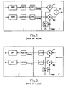
- Fig. 1 shows the signal processing path of a conventional one Transmitting device, which is used, for example, in mobile telephones place. From an implementation point of view the transmission signal path from a first section 1, which is realized in the form of a baseband chip, and one second section 2, which is in the form of a high-frequency chip is present together.
- Modulated data signal is generated using two digital Signal processors DSP1 and DSP2 separately for the I and Q branch of signal preprocessing (rate conversion and interpolation steps).
- the on thus generated I and Q signal components of the modulated Signals are converted into digital-to-analog converters DAC1 and DAC2 are each converted into analog baseband signals.
- DAC1 and DAC2 are each converted into analog baseband signals.
- LPF1 or LPF2 Low-pass filtering the low pass filter LPF1 or LPF2.
- the modulated, analog and low-pass filtered I and Q signal components are used for carrier signal conversion via the so-called I / Q interface into the high frequency signal processing section 2 entered.
- the carrier signal conversion takes place there mixing up the analog I and Q signal components in Mixers M1 and M2 ideally use two 90 ° phase-shifted straps.
- the mixers M1 and M2 Modulated carrier signals are generated in a summation stage S superimposed on each other and as a high-frequency signal radiated via an antenna (not shown).
- the conventional receiving device shown in Fig. 2 performs essentially an inverse signal processing by. Under The receiving device can implement the same aspects two chips (RF chip and baseband chip) as the transmitter be realized, the corresponding ones in FIG Signal processing sections 1 'and 2' of the reception path are shown within the respective chips.
- Fig. 2 The same or comparable parts as in Fig. 1 are in Fig. 2 labeled with the same reference numerals. That about one Antenna received modulated carrier signal (not shown) is in the baseband or using mixers M1 and M2 mixed down to an intermediate frequency position.
- the mixer M1, M2 are in turn separated by two orthogonal ones Carrier operated, which by means of a phase shifter PS be generated in a single carrier.
- the one from the phase shifter PS caused phase shift is also here Ideally 90 °.
- the I and Q signal components generated by mixers M1 and M2 are used in analog low pass filters LPF3, LPF4 respectively subjected to low pass filtering and then via the I / Q interface (by the shown in Fig. 2 Dividing line between sections 1 'and 2' indicated) Signal processing section 1 'fed in the baseband chip.
- There the I-signal components are made using an analog-to-digital Converter ADC1 and the Q signal component by means of a Analog-to-digital converter ADC2 converted into digital signals.
- Another channel filtering is done by two separate ones digital filters DF1 and DF2 guaranteed.
- ⁇ is called a phase error designated.
- the phase error ⁇ can be caused by the phase shifter PS, but also by other signal processing elements, not shown or influencing factors in the shown Sending or receiving devices are caused.
- phase error ⁇ in the receiving direction causes a disturbance in the received signal, which leads to an increase in the bit error rate (with a fixed Signal-to-noise ratio).
- bit error rate with a fixed Signal-to-noise ratio
- FIGS. 1 and 2 show transmitting and receiving devices, in which in the manner according to the invention a correction of the phase error made in the digital signal processing area becomes.
- the essential Difference between those shown in Figs. 1 and 5 Transmitting equipment is that in the signal paths between the digital signal processors DSP1, DSP2 and the digital-to-analog converters DAC1, DAC2 a phase correction stage PC is provided.
- the corresponding signal processing section in the baseband chip is with the reference symbol 10 'designated.
- the essential is analogous Difference between those in FIG. 2 and FIG. 6 receiving devices shown that preferably in the signal path behind the digital filters DF1, DF2 Phase correction stage PC connects, with the changed here Signal processing section in the baseband with the reference symbol 10 is designated.
- Phase correction stages PC can be identical. Hereinafter its mode of action is explained:
- phase error present in the equivalent baseband can be modeled using the following matrix operation:
- I 0 and Q 0 denote carrier signals with the optimal phase difference of 90 °, and I and Q denote the phase error-prone I and Q signal components.
- This phase error ⁇ is now ideally completely reversed in the receive path and / or also in the transmit path by the following matrix operation.
- phase correction stage PC This calculation rule is carried out by the phase correction stage PC.
- a (theoretically) exact correction of the phase error is, however, not necessary in most cases.
- digital phase correction is implemented with significantly less computational effort. This applies both to the phase correction stage PC in the transmitting device and to the phase correction stage PC in the receiving device.
- the phase error ⁇ to be used in the phase correction stage PC can be determined in various ways.
- a first possibility is that the phase error ⁇ to be corrected is determined once and is programmed into the phase correction stage PC during the initial assembly of the device. The device is then phase error compensated for further operation.
- the determination of the phase error .DELTA..phi. Can be determined in a device-related manner by measuring the phase error .DELTA..phi. Actually occurring in the respective device or also statistically using a measurement of the phase errors of a large number of devices of the same type or series.
- phase error ⁇ can also carried out as part of a check or maintenance of the device become.
- FIG. 7 shows a representation comparable to FIGS. 3 and 4 the phase relationship between the I and Q signal components the baseband signal according to the first name of an inventive Phase error compensation.
- a difference to the ideal complex sine signal with a phase difference of exactly 90 ° cannot be seen, compare Fig. 3.
Landscapes
- Engineering & Computer Science (AREA)
- Computer Networks & Wireless Communication (AREA)
- Signal Processing (AREA)
- Power Engineering (AREA)
- Digital Transmission Methods That Use Modulated Carrier Waves (AREA)
Claims (6)
- Procédé de compensation d'une erreur de phase dans un système d'émission avec branches de traitement de signal l et Q,
caractérisé par les étapes suivantes :programmation d'une erreur de phase Δ, préalablement déterminée par mesure, d'un étage d'émission à haute fréquence utilisé dans le système d'émission pendant le premier montage ou la maintenance du système d'émission dans le tronçon de traitement de signal numérique du système d'émission ; etcalcul des composantes de signal l et Q à phase corrigée dans un tronçon de traitement de signal numérique des branches de traitement de signal l et Q pendant le fonctionnement en émission par correction de composantes de signal l et Q avec l'erreur de phase Δ constante programmée. - Procédé de compensation d'une erreur de phase dans un système de réception avec branches de traitement de signal l et Q,
caractérisé par les étapes suivantes :programmation d'une erreur de phase Δ, préalablement déterminée par mesure, d'un étage de réception à haute fréquence utilisé dans le système de réception pendant le premier montage ou la maintenance du système de réception dans le tronçon de traitement de signal numérique du système de réception ; etcalcul des composantes de signal l et Q à phase corrigée dans un tronçon de traitement de signal numérique des branches de traitement de signal l et Q du système de réception pendant le fonctionnement en réception par correction des composantes de signal l et Q entachées d'une erreur de phase avec l'erreur de phase Δ constante programmée. - Procédé selon la revendication 1 ou 2,
caractérisé par le fait aue le calcul s'effectue selonou selon une approximation de cette équation, l et Q étant les composantes de signal I et Q entachées d'une erreur de phase, I (Δ) et Q (Δ) étant les composantes de signal l et Q à erreur de phase compensée et Δ étant l'erreur de phase utilisée pour la correction.
- Procédé selon la revendication 3,
caractérisé par le fait que le calcul s'effectue selon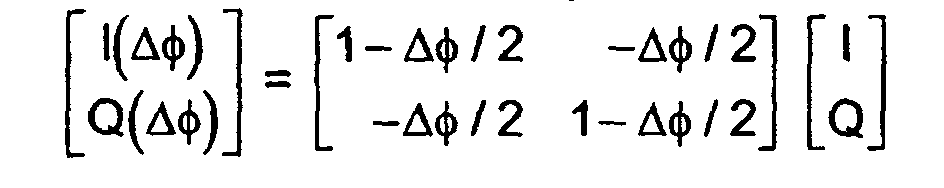
- Procédé selon l'une des revendications précédentes,
caractérisé par l'étape :détermination d'une valeur pour l'erreur de phase Δ utilisée pour la correction par un procédé statistique basé sur des mesures des erreurs de phase de plusieurs étages d'émission à haute fréquence ou d'étages de réception à haute fréquence. - Procédé selon l'une des revendications précédentes,
caractérisé par l'étape :détermination d'une valeur pour l'erreur de phase Δ utilisée pour la correction par une mesure de l'erreur de phase d'un certain étage d'émission à haute fréquence ou d'un certain étage de réception à haute fréquence.
Applications Claiming Priority (3)
| Application Number | Priority Date | Filing Date | Title |
|---|---|---|---|
| DE10136071 | 2001-07-25 | ||
| DE10136071A DE10136071A1 (de) | 2001-07-25 | 2001-07-25 | Verfahren und Vorrichtung zur Kompensation eines Phasenfehlers eines Empfangs- und/oder Sendesystems mit I/Q-Schnittstelle |
| PCT/DE2002/002356 WO2003013191A2 (fr) | 2001-07-25 | 2002-06-27 | Procede et dispositif pour compenser une erreur de phase de systeme de reception et/ou d'emission a interface i & q |
Publications (3)
| Publication Number | Publication Date |
|---|---|
| EP1410496A2 EP1410496A2 (fr) | 2004-04-21 |
| EP1410496B1 true EP1410496B1 (fr) | 2004-11-24 |
| EP1410496B2 EP1410496B2 (fr) | 2016-07-13 |
Family
ID=7692942
Family Applications (1)
| Application Number | Title | Priority Date | Filing Date |
|---|---|---|---|
| EP02750811.8A Expired - Lifetime EP1410496B2 (fr) | 2001-07-25 | 2002-06-27 | Procédé et dispositif pour compenser une erreur de phase de système de réception et/ou d'émission à interface i & q |
Country Status (5)
| Country | Link |
|---|---|
| US (1) | US20040172438A1 (fr) |
| EP (1) | EP1410496B2 (fr) |
| CN (1) | CN100355202C (fr) |
| DE (2) | DE10136071A1 (fr) |
| WO (1) | WO2003013191A2 (fr) |
Families Citing this family (6)
| Publication number | Priority date | Publication date | Assignee | Title |
|---|---|---|---|---|
| CN100508411C (zh) * | 2004-06-23 | 2009-07-01 | 瑞昱半导体股份有限公司 | 同相信号与正交相信号不匹配的校正单元及方法 |
| US7738572B2 (en) | 2004-10-11 | 2010-06-15 | Realtek Semiconductor Corp. | Orthogonal frequency division multiplexing (OFDM) receiver capable of correcting in-phase and quadrature-phase mismatch and method thereof |
| CN103731382B (zh) * | 2012-10-12 | 2017-06-30 | 北京信威通信技术股份有限公司 | 一种终端iq不平衡的校正方法 |
| DE102014113922B4 (de) * | 2014-09-25 | 2021-10-14 | Apple Inc. | Digital-zu-Analog-Wandler-Schaltungen, Sender und Verfahren zum Erzeugen eines Hochfrequenz-Sendesignals und Verfahren einer Digital-zu-Analog-Umwandlung |
| CN107193000B (zh) * | 2017-05-19 | 2021-01-15 | 南京矽力微电子技术有限公司 | 物体特征检测装置和方法 |
| WO2020125790A1 (fr) | 2018-12-21 | 2020-06-25 | Huawei Technologies Co., Ltd. | Émetteur polaire à compensation de fuite |
Family Cites Families (16)
| Publication number | Priority date | Publication date | Assignee | Title |
|---|---|---|---|---|
| US4843584A (en) * | 1987-02-05 | 1989-06-27 | Malaiperumal Sundaramurthy | Cordic implementation of multi-dimensional plane rotation over the complex field |
| EP0378719B1 (fr) * | 1989-01-18 | 1994-04-27 | Siemens Aktiengesellschaft | Générateur de distorsions numérique |
| US5105195A (en) † | 1990-12-10 | 1992-04-14 | Hughes Aircraft Company | System and method for compensation of in-phase and quadrature phase and gain imbalance |
| US5111155A (en) * | 1991-03-04 | 1992-05-05 | Motorola, Inc. | Distortion compensation means and method |
| GB9109617D0 (en) † | 1991-05-03 | 1991-06-26 | Texas Instruments Ltd | Method and apparatus for signal processing |
| FR2680923B1 (fr) † | 1991-08-30 | 1996-11-22 | Patrick Vandamme | Dispositif de demodulation coherente a circuit numerique de recuperation d'onde porteuse. |
| GB2262006B (en) * | 1991-11-30 | 1995-06-21 | Technophone Ltd | Digital radio modulator |
| US5604768A (en) † | 1992-01-09 | 1997-02-18 | Cellnet Data Systems, Inc. | Frequency synchronized bidirectional radio system |
| US5550869A (en) * | 1992-12-30 | 1996-08-27 | Comstream Corporation | Demodulator for consumer uses |
| DE69614284T2 (de) * | 1995-02-02 | 2002-01-10 | Nippon Telegraph And Telephone Corp., Tokio/Tokyo | Verzerrungskorrekturvorrichtung |
| JP2967699B2 (ja) † | 1995-03-06 | 1999-10-25 | 日本電気株式会社 | 送信装置 |
| JPH10508406A (ja) * | 1995-08-30 | 1998-08-18 | フィリップス エレクトロニクス ネムローゼ フェンノートシャップ | 低複雑性信号処理装置及びその信号処理装置を具えた受信機 |
| US5705949A (en) * | 1996-09-13 | 1998-01-06 | U.S. Robotics Access Corp. | Compensation method for I/Q channel imbalance errors |
| WO1999005784A1 (fr) † | 1997-07-28 | 1999-02-04 | Rohde & Schwarz Gmbh & Co. Kg | Procede et dispositif de mesure pour la mesure de la distorsion d'un amplificateur de puissance haute frequence, ainsi que procede et dispositif de correction pour la correction automatique d'un amplificateur de puissance haute frequence |
| JP3822057B2 (ja) † | 1999-04-02 | 2006-09-13 | 三菱電機株式会社 | 移動通信端末装置 |
| US6661852B1 (en) * | 1999-07-21 | 2003-12-09 | Raytheon Company | Apparatus and method for quadrature tuner error correction |
-
2001
- 2001-07-25 DE DE10136071A patent/DE10136071A1/de not_active Withdrawn
-
2002
- 2002-06-27 DE DE50201641T patent/DE50201641D1/de not_active Expired - Lifetime
- 2002-06-27 CN CNB028148789A patent/CN100355202C/zh not_active Expired - Lifetime
- 2002-06-27 EP EP02750811.8A patent/EP1410496B2/fr not_active Expired - Lifetime
- 2002-06-27 WO PCT/DE2002/002356 patent/WO2003013191A2/fr not_active Ceased
-
2004
- 2004-01-16 US US10/758,795 patent/US20040172438A1/en not_active Abandoned
Also Published As
| Publication number | Publication date |
|---|---|
| DE10136071A1 (de) | 2003-02-13 |
| CN100355202C (zh) | 2007-12-12 |
| US20040172438A1 (en) | 2004-09-02 |
| WO2003013191A3 (fr) | 2003-08-21 |
| CN1535498A (zh) | 2004-10-06 |
| DE50201641D1 (de) | 2004-12-30 |
| EP1410496B2 (fr) | 2016-07-13 |
| WO2003013191A2 (fr) | 2003-02-13 |
| EP1410496A2 (fr) | 2004-04-21 |
Similar Documents
| Publication | Publication Date | Title |
|---|---|---|
| DE69736188T2 (de) | Verfahren in einem digitalen quadraturmodulator und -demodulator sowie digitaler quadraturmodulator und -demodulator | |
| DE102014218909A1 (de) | Kommunikationseinheit und Verfahren zum Bestimmen und/oder Kompensieren von frequenzabhängiger Quadraturfehlanpassung | |
| EP1410496B1 (fr) | Procede et dispositif pour compenser une erreur de phase de systeme de reception et/ou d'emission a interface i & q | |
| EP1317830B1 (fr) | Procede de production de signaux de communication mobile de differentes normes de telephonie mobile | |
| EP1639377A1 (fr) | Systeme de mesure haute frequence avec modules haute frequence spatialement separes | |
| WO2020058049A1 (fr) | Procédé et dispositif pour convertir un signal d'entrée analogique en un signal de sortie numérique | |
| EP1523144A2 (fr) | Procédé et circuit de détermination d'un symbole dans l'espace complexe de phase d'un procédé de modulation en quadrature | |
| DE60027314T2 (de) | Einrichtung zur unterdrückung der spiegelfrequenz | |
| DE102006017937B4 (de) | Verfahren und Kalibrierungssytem für IQ-Gleichspannungsoffset- und Unsymmetrie-Kalibrierung durch Verwendung von analytischen Formeln, um gewünschte Kompensationswerte schnell zu bestimmen | |
| EP0778996A1 (fr) | Procede et dispositif permettant de remettre en forme des paires de signaux | |
| EP1892910A2 (fr) | Procédé ou circuit destiné à déterminer un symbole lors de la réception d'un signal coupé avec une paire de signaux à quadrature | |
| DE10036889C1 (de) | Verfahren und Einrichtung zur Bestimmung eines in einem differentiellen Sendesignalabschnitt eines Funkgerätes auftretenden Offsetwerts | |
| DE102010064614B3 (de) | Verfahren und Vorrichtung zum Modifizieren einer Charakteristik eines komplexwertigen Signals | |
| WO2003023948A2 (fr) | Dispositif d'emission destine notamment a la telephonie mobile | |
| DE102016102005B4 (de) | Schaltungsanordnung und Verfahren zur Erzeugung eines hochfrequenten, analogen Sendesignals | |
| DE19933266A1 (de) | Vorrichtung zum Empfangen von Funksignalen | |
| DE102006001650B4 (de) | Signalverarbeitungseinrichtung, Verwendung der Signalverarbeitungseinrichtung und Verfahren zur Signalverarbeitung | |
| EP1527524B1 (fr) | Systeme de transmission, en particulier pour la radiotelephonie mobile | |
| DE10335044B4 (de) | Demodulationsanordnung für ein Funksignal | |
| DE10361651A1 (de) | Verstärkeranordnung sowie Verfahren zum Kalibrieren einer Verstärkeranordnung | |
| DE10252099A1 (de) | Messgerät und Verfahren zum Ermitteln einer Kennlinie einer Hochfrequenzeinheit | |
| DE102008049666B4 (de) | Digitale Modulation | |
| WO2003043206A2 (fr) | Dispositif emetteur destine notamment a la telephonie mobile | |
| DE102008010254B4 (de) | Empfangsschaltung und Verfahren zum Empfangen eines Signals einer Amplitudenumtastung | |
| WO1999066687A1 (fr) | Demodulation a coherence diferentielle de signaux dbpsk |
Legal Events
| Date | Code | Title | Description |
|---|---|---|---|
| PUAI | Public reference made under article 153(3) epc to a published international application that has entered the european phase |
Free format text: ORIGINAL CODE: 0009012 |
|
| 17P | Request for examination filed |
Effective date: 20040107 |
|
| AK | Designated contracting states |
Kind code of ref document: A2 Designated state(s): DE DK FI FR GB IT SE |
|
| GRAP | Despatch of communication of intention to grant a patent |
Free format text: ORIGINAL CODE: EPIDOSNIGR1 |
|
| RIN1 | Information on inventor provided before grant (corrected) |
Inventor name: GUNZELMANN, BERTRAM |
|
| GRAS | Grant fee paid |
Free format text: ORIGINAL CODE: EPIDOSNIGR3 |
|
| GRAA | (expected) grant |
Free format text: ORIGINAL CODE: 0009210 |
|
| AK | Designated contracting states |
Kind code of ref document: B1 Designated state(s): DE DK FI FR GB IT SE |
|
| PG25 | Lapsed in a contracting state [announced via postgrant information from national office to epo] |
Ref country code: IT Free format text: LAPSE BECAUSE OF FAILURE TO SUBMIT A TRANSLATION OF THE DESCRIPTION OR TO PAY THE FEE WITHIN THE PRESCRIBED TIME-LIMIT;WARNING: LAPSES OF ITALIAN PATENTS WITH EFFECTIVE DATE BEFORE 2007 MAY HAVE OCCURRED AT ANY TIME BEFORE 2007. THE CORRECT EFFECTIVE DATE MAY BE DIFFERENT FROM THE ONE RECORDED. Effective date: 20041124 Ref country code: GB Free format text: LAPSE BECAUSE OF FAILURE TO SUBMIT A TRANSLATION OF THE DESCRIPTION OR TO PAY THE FEE WITHIN THE PRESCRIBED TIME-LIMIT Effective date: 20041124 Ref country code: FI Free format text: LAPSE BECAUSE OF FAILURE TO SUBMIT A TRANSLATION OF THE DESCRIPTION OR TO PAY THE FEE WITHIN THE PRESCRIBED TIME-LIMIT Effective date: 20041124 |
|
| REG | Reference to a national code |
Ref country code: GB Ref legal event code: FG4D Free format text: NOT ENGLISH |
|
| REF | Corresponds to: |
Ref document number: 50201641 Country of ref document: DE Date of ref document: 20041230 Kind code of ref document: P |
|
| PG25 | Lapsed in a contracting state [announced via postgrant information from national office to epo] |
Ref country code: DK Free format text: LAPSE BECAUSE OF FAILURE TO SUBMIT A TRANSLATION OF THE DESCRIPTION OR TO PAY THE FEE WITHIN THE PRESCRIBED TIME-LIMIT Effective date: 20050224 Ref country code: SE Free format text: LAPSE BECAUSE OF FAILURE TO SUBMIT A TRANSLATION OF THE DESCRIPTION OR TO PAY THE FEE WITHIN THE PRESCRIBED TIME-LIMIT Effective date: 20050224 |
|
| PLAQ | Examination of admissibility of opposition: information related to despatch of communication + time limit deleted |
Free format text: ORIGINAL CODE: EPIDOSDOPE2 |
|
| PLBI | Opposition filed |
Free format text: ORIGINAL CODE: 0009260 |
|
| PLBQ | Unpublished change to opponent data |
Free format text: ORIGINAL CODE: EPIDOS OPPO |
|
| 26 | Opposition filed |
Opponent name: ROHDE & SCHWARZ GMBH & CO KG Effective date: 20050414 |
|
| GBV | Gb: ep patent (uk) treated as always having been void in accordance with gb section 77(7)/1977 [no translation filed] |
Effective date: 20041124 |
|
| PLAX | Notice of opposition and request to file observation + time limit sent |
Free format text: ORIGINAL CODE: EPIDOSNOBS2 |
|
| ET | Fr: translation filed | ||
| PLBB | Reply of patent proprietor to notice(s) of opposition received |
Free format text: ORIGINAL CODE: EPIDOSNOBS3 |
|
| RAP2 | Party data changed (patent owner data changed or rights of a patent transferred) |
Owner name: INFINEON TECHNOLOGIES AG |
|
| RDAF | Communication despatched that patent is revoked |
Free format text: ORIGINAL CODE: EPIDOSNREV1 |
|
| APBM | Appeal reference recorded |
Free format text: ORIGINAL CODE: EPIDOSNREFNO |
|
| APBP | Date of receipt of notice of appeal recorded |
Free format text: ORIGINAL CODE: EPIDOSNNOA2O |
|
| APAH | Appeal reference modified |
Free format text: ORIGINAL CODE: EPIDOSCREFNO |
|
| REG | Reference to a national code |
Ref country code: FR Ref legal event code: TP Owner name: INFINEON TECHNOLOGIES DELTA GMBH, DE Effective date: 20111102 |
|
| RAP2 | Party data changed (patent owner data changed or rights of a patent transferred) |
Owner name: INFINEON TECHNOLOGIES DELTA GMBH |
|
| APBQ | Date of receipt of statement of grounds of appeal recorded |
Free format text: ORIGINAL CODE: EPIDOSNNOA3O |
|
| REG | Reference to a national code |
Ref country code: FR Ref legal event code: TP Owner name: INTEL MOBILE COMMUNICATIONS GMBH, DE Effective date: 20120404 |
|
| RAP2 | Party data changed (patent owner data changed or rights of a patent transferred) |
Owner name: INTEL MOBILE COMMUNICATIONS TECHNOLOGY GMBH |
|
| RAP2 | Party data changed (patent owner data changed or rights of a patent transferred) |
Owner name: INTEL MOBILE COMMUNICATIONS GMBH |
|
| REG | Reference to a national code |
Ref country code: DE Ref legal event code: R081 Ref document number: 50201641 Country of ref document: DE Owner name: INTEL MOBILE COMMUNICATIONS GMBH, DE Free format text: FORMER OWNER: INFINEON TECHNOLOGIES AG, 81669 MUENCHEN, DE Effective date: 20130306 Ref country code: DE Ref legal event code: R081 Ref document number: 50201641 Country of ref document: DE Owner name: INTEL MOBILE COMMUNICATIONS GMBH, DE Free format text: FORMER OWNER: INFINEON TECHNOLOGIES DELTA GMBH, 85579 NEUBIBERG, DE Effective date: 20130306 Ref country code: DE Ref legal event code: R081 Ref document number: 50201641 Country of ref document: DE Owner name: INTEL MOBILE COMMUNICATIONS GMBH, DE Free format text: FORMER OWNER: INTEL MOBILE COMMUNICATIONS TECHNOLOGY GMBH, 85579 NEUBIBERG, DE Effective date: 20130306 |
|
| PLBP | Opposition withdrawn |
Free format text: ORIGINAL CODE: 0009264 |
|
| APBU | Appeal procedure closed |
Free format text: ORIGINAL CODE: EPIDOSNNOA9O |
|
| REG | Reference to a national code |
Ref country code: FR Ref legal event code: PLFP Year of fee payment: 14 |
|
| RAP2 | Party data changed (patent owner data changed or rights of a patent transferred) |
Owner name: INTEL DEUTSCHLAND GMBH |
|
| RIC2 | Information provided on ipc code assigned after grant |
Ipc: H03D 3/00 20060101AFI20160120BHEP Ipc: H04L 27/00 20060101ALI20160120BHEP Ipc: H03C 3/40 20060101ALI20160120BHEP |
|
| REG | Reference to a national code |
Ref country code: FR Ref legal event code: PLFP Year of fee payment: 15 |
|
| PUAH | Patent maintained in amended form |
Free format text: ORIGINAL CODE: 0009272 |
|
| STAA | Information on the status of an ep patent application or granted ep patent |
Free format text: STATUS: PATENT MAINTAINED AS AMENDED |
|
| 27A | Patent maintained in amended form |
Effective date: 20160713 |
|
| AK | Designated contracting states |
Kind code of ref document: B2 Designated state(s): DE DK FI FR GB IT SE |
|
| REG | Reference to a national code |
Ref country code: DE Ref legal event code: R102 Ref document number: 50201641 Country of ref document: DE |
|
| REG | Reference to a national code |
Ref country code: FR Ref legal event code: PLFP Year of fee payment: 16 |
|
| REG | Reference to a national code |
Ref country code: FR Ref legal event code: PLFP Year of fee payment: 17 |
|
| REG | Reference to a national code |
Ref country code: DE Ref legal event code: R082 Ref document number: 50201641 Country of ref document: DE Representative=s name: BARDEHLE PAGENBERG PARTNERSCHAFT MBB PATENTANW, DE Ref country code: DE Ref legal event code: R081 Ref document number: 50201641 Country of ref document: DE Owner name: APPLE INC., CUPERTINO, US Free format text: FORMER OWNER: INTEL MOBILE COMMUNICATIONS GMBH, 85579 NEUBIBERG, DE |
|
| PGFP | Annual fee paid to national office [announced via postgrant information from national office to epo] |
Ref country code: DE Payment date: 20210602 Year of fee payment: 20 Ref country code: FR Payment date: 20210513 Year of fee payment: 20 |
|
| REG | Reference to a national code |
Ref country code: DE Ref legal event code: R071 Ref document number: 50201641 Country of ref document: DE |