EP1411423A2 - Berührungsempfindliche Tafel - Google Patents
Berührungsempfindliche Tafel Download PDFInfo
- Publication number
- EP1411423A2 EP1411423A2 EP03022154A EP03022154A EP1411423A2 EP 1411423 A2 EP1411423 A2 EP 1411423A2 EP 03022154 A EP03022154 A EP 03022154A EP 03022154 A EP03022154 A EP 03022154A EP 1411423 A2 EP1411423 A2 EP 1411423A2
- Authority
- EP
- European Patent Office
- Prior art keywords
- movable plate
- supporting substrate
- substrate
- piezoelectric substrate
- pair
- Prior art date
- Legal status (The legal status is an assumption and is not a legal conclusion. Google has not performed a legal analysis and makes no representation as to the accuracy of the status listed.)
- Withdrawn
Links
Images



Classifications
-
- G—PHYSICS
- G06—COMPUTING OR CALCULATING; COUNTING
- G06F—ELECTRIC DIGITAL DATA PROCESSING
- G06F3/00—Input arrangements for transferring data to be processed into a form capable of being handled by the computer; Output arrangements for transferring data from processing unit to output unit, e.g. interface arrangements
- G06F3/01—Input arrangements or combined input and output arrangements for interaction between user and computer
- G06F3/03—Arrangements for converting the position or the displacement of a member into a coded form
- G06F3/041—Digitisers, e.g. for touch screens or touch pads, characterised by the transducing means
- G06F3/0416—Control or interface arrangements specially adapted for digitisers
- G06F3/04164—Connections between sensors and controllers, e.g. routing lines between electrodes and connection pads
-
- G—PHYSICS
- G06—COMPUTING OR CALCULATING; COUNTING
- G06F—ELECTRIC DIGITAL DATA PROCESSING
- G06F3/00—Input arrangements for transferring data to be processed into a form capable of being handled by the computer; Output arrangements for transferring data from processing unit to output unit, e.g. interface arrangements
- G06F3/01—Input arrangements or combined input and output arrangements for interaction between user and computer
- G06F3/03—Arrangements for converting the position or the displacement of a member into a coded form
-
- G—PHYSICS
- G06—COMPUTING OR CALCULATING; COUNTING
- G06F—ELECTRIC DIGITAL DATA PROCESSING
- G06F3/00—Input arrangements for transferring data to be processed into a form capable of being handled by the computer; Output arrangements for transferring data from processing unit to output unit, e.g. interface arrangements
- G06F3/01—Input arrangements or combined input and output arrangements for interaction between user and computer
- G06F3/03—Arrangements for converting the position or the displacement of a member into a coded form
- G06F3/041—Digitisers, e.g. for touch screens or touch pads, characterised by the transducing means
-
- G—PHYSICS
- G06—COMPUTING OR CALCULATING; COUNTING
- G06F—ELECTRIC DIGITAL DATA PROCESSING
- G06F3/00—Input arrangements for transferring data to be processed into a form capable of being handled by the computer; Output arrangements for transferring data from processing unit to output unit, e.g. interface arrangements
- G06F3/01—Input arrangements or combined input and output arrangements for interaction between user and computer
- G06F3/03—Arrangements for converting the position or the displacement of a member into a coded form
- G06F3/041—Digitisers, e.g. for touch screens or touch pads, characterised by the transducing means
- G06F3/045—Digitisers, e.g. for touch screens or touch pads, characterised by the transducing means using resistive elements, e.g. a single continuous surface or two parallel surfaces put in contact
Definitions
- the present invention relates to a wiring structure of a touch panel used in a touch-panel input device that gives a feeling of input manipulation to a manipulator when he/she presses a movable plate by allowing the movable plate being pressed or a supporting substrate supporting the movable plate to vibrate.
- the present invention relates to a wiring structure of a touch panel in the case of allowing the movable plate or the supporting substrate to vibrate using a piezoelectric substrate.
- a touch panel is used in a touch-panel input device.
- the touch-panel input device is a device in which a movable plate and a supporting substrate are deposited with a slight insulation gap between conductive layers formed on their respective opposing surfaces. When the movable plate is pressed, the touch-panel input device electrically detects that the opposing conductive layers come in contact with each other at the pressed position, and outputs the pressed position data to each processing device.
- the touch-panel input device of this kind has a lamination structure in which the movable plate and the supporting substrate are deposited with a slight insulation gap in between.
- the pressing stroke of the movable plate is in an extremely small range from tens to hundreds microns, which makes it difficult to give a feeling of input manipulation to the manipulator.
- a force feedback type touch panel is adopted, in which the movable plate or the supporting substrate is allowed to vibrate when the movable plate is pressed, so that the manipulator has a feeling of input manipulation at his fingertip pressing the movable plate.
- Japanese Patent Application No. 2001-312399 Japanese Patent Application No. 2001-312399 describing a device as follows, which is related to a touch panel that allows the movable plate or the supporting substrate to vibrate in such a manner that the manipulator can detect the vibration, using a simple driving circuit.
- this earlier development discloses a touch-panel input device arranged in such a manner that a pair of driving electrodes is fixed to the respective opposing surfaces of the piezoelectric substrate, and the piezoelectric substrate is fixed to the movable plate or the supporting substrate directly or through the driving electrodes.
- the movable plate or the supporting substrate is allowed to vibrate by the piezoelectric substrate that expands and contracts in association with application of a driving voltage to the pair of driving electrodes.
- the present invention relates to an improvement of the wiring structure of the touch panel of the previous development described in the above patent application.
- a touch panel having the structure of depositing the movable plate on the back surface of which is formed a conductive layer and a supporting substrate on the top surface of which is formed a conductive layer with a slight wiring gap in between, and fixing the piezoelectric substrate to the movable plate or the supporting substrate, it is necessary to withdraw a wiring to the movable plate and the supporting substrate and a driving wiring for the piezoelectric substrate.
- neither the structure of merely sandwiching the piezoelectric substrate between the movable plate and the supporting substrate nor the method of fixing the piezoelectric substrate to the back surface of the supporting substrate can reduce the thickness of the touch panel sufficiently.
- a structure for a touch panel including: a movable plate having an input manipulation surface on a main surface thereof; a supporting substrate, disposed with a slight insulation gap from the movable plate, for supporting the movable plate from a back surface thereof; conductive layers formed on the movable plate and the supporting substrate on their respective opposing surfaces; and a piezoelectric substrate fixed to one of the movable plate and the supporting substrate and provided with a pair of driving electrodes fixed to respective opposing surfaces thereof, a conductive layer electrode of the movable plate, a conductive layer electrode of the supporting substrate, and the pair of driving electrodes of the piezoelectric substrate are withdrawn integrally using a single connector tail.
- to withdraw integrally using a single connector tail means that a plurality of connectors are not connected separately to the touch panel.
- the connector tail is a component obtained by forming a copper-foil plated wiring pattern on an insulative tail base material, such as polyethylene terephthalate (PET), and then covering the wiring pattern with a tail protection sheet material.
- an insulative tail base material such as polyethylene terephthalate (PET)
- the conductive layer electrode of the movable plate, the conductive layer electrode of the supporting substrate, and the pair of driving electrodes of the piezoelectric substrate are withdrawn integrally using the single connector tail in contrast to the conventional method by which leads from the conductive electrodes of the movable plate and the supporting substrate and a lead used to apply a voltage to the driving electrodes of the piezoelectric substrate are provided separately and connected to their respective connectors. Consequently, the number of components can be reduced and the structure can be simpler, which can in turn reduce the weight and the size of the touch panel.
- the connectors are withdrawn integrally by providing a cut to a single connector tail base material to be divided into a portion to be connected to the conductive layer electrodes of the movable plate and the supporting substrate and a portion to be connected to the pair of driving electrodes formed on the respective opposing surfaces of the piezoelectric substrate.
- the second aspect of the invention by providing a cut to the single connector tail base material, it is possible to withdraw the electrodes integrally using, for example, a standard connector tail having eight lines in a single tail base material.
- one of the pair of electrodes formed on the respective opposing surfaces of the piezoelectric substrate is folded back at one end in a longitudinal direction to be provided on a same surface of the piezoelectric substrate where the other electrode is provided, with a gap in between. Consequently, the pair of the electrodes can be connected to the leads on one surface of the piezoelectric substrate.
- one of the pair of electrodes formed on the respective opposing surfaces of the piezoelectric substrate is folded back at one end in a longitudinal direction to be provided on a same surface of the piezoelectric substrate where the other electrode is provided, with a gap in between. Consequently, lead wirings of the both electrodes can be withdrawn from one surface of the piezoelectric substrate, which can in turn reduce the thickness of the touch panel structure.
- the connector tail can be connected to the both surfaces of the piezoelectric substrate through direct soldering or using a conductive bonding agent.
- a notch portion is provided in an edge portion of the supporting substrate or a concave portion is formed in a side portion of the supporting substrate, and the piezoelectric substrate is provided in the notch portion or the concave portion. Consequently, the thickness of the touch panel can be reduced.
- the piezoelectric substrate thinner than the supporting substrate is used, and the notch portion is provided in the edge portion of the supporting substrate or the concave portion is formed in the side portion of the supporting substrate, and the piezoelectric substrate is accommodated in the notch portion or the concave portion. Consequently, the thickness of the entire touch panel product can be reduced; moreover, because a protrusion formed by the piezoelectric substrate can be eliminated, flaws or damage of the product caused by the protrusion can be prevented.
- one of the pair of electrodes formed on the respective opposing surfaces of the piezoelectric substrate is folded back at one end in a longitudinal direction to be provided on a same surface of the piezoelectric substrate where the other electrode is provided, with a gap in between; a pair of lead wiring patterns is formed on a back surface of the supporting substrate through conductive printing; and the pair of electrodes of the piezoelectric substrate is bonded to one end of the pair of lead wiring patterns using a conductive bonding agent, and the connector tail is connected to the other end through thermocompression.
- the connector tail can be connected to the respective electrodes through thermocompression using the wiring patterns, which can contribute to a reduction of the touch panel in size.
- the pair of lead wiring patterns is formed on the back surface of the supporting substrate through conductive printing, so that one of the pair of wiring patterns can be connected to the piezoelectric substrate and the other is connected to the connector tail through thermocompression. Consequently, the routing structure from the respective electrodes can be simpler, and hence the size of the product can be reduced.
- the width of a spacer member (adhesive agent layer) can be reduced in comparison with a case where the piezoelectric substrate is sandwiched between the movable plate and the supporting substrate, which makes it possible to secure a larger effective area of the touch panel.
- the touch panel comprises: a movable plate having an input manipulation surface on a main surface thereof; a supporting substrate, disposed with a slight insulation gap from the movable plate, for supporting the movable plate from a back surface thereof; conductive layers formed on the movable plate and the supporting substrate on their respective opposing surfaces; and a piezoelectric substrate fixed to one of the movable plate and the supporting substrate and provided with a pair of driving electrodes fixed to respective opposing surfaces thereof, a conductive layer electrode of one of the movable plate and the supporting substrate is connected to the electrodes of the piezoelectric substrate, and leads from the movable plate and the supporting substrate are formed using a connector tail.
- the sixth aspect of the invention by providing a structure in which the pair of the electrodes of the piezoelectric substrate is connected to the conductive layer electrode of the movable plate or the supporting substrate, part of the driving electrode wiring of the piezoelectric substrate can be shared with the lead of the movable plate or the supporting substrate, which can in turn reduce the weight and the size of the touch panel.
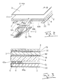
- Fig. 1 is a view showing an outward appearance of a touch panel 1 of the invention. Wiring is provided by leading a single connector tail 7 from the touch panel 1.
- Fig. 2 is a view showing a wiring structure of a connector tail portion.
- Fig. 3 is a cross section, taken along the line A-A of Fig. 2, showing details of the wiring structure.
- Fig. 4 is a cross section, taken along the line B-B of Fig. 2 , showing details of the wiring structure.
- a movable plate 3 is a molded flexible rectangular sheet made of transparent synthetic resin, and PET (polyethylene terephthalate) is used herein.
- the movable plate 3 can be made of an arbitrary material as long as it can slightly bend toward a supporting substrate 4 described below. It should be noted, however, that in the case of making a display portion (not shown) formed inside the supporting substrate 4 visible like in this embodiment, a transparent material is used. Alternatively, in a case where rigidity of a certain degree is needed, a glass substrate or an acrylic plate can be used, and in a case where flexibility is desired, PC (polycarbonate), PES (polyether sulfone), PI (polyimide), etc. can be used.
- a transparent hard coating agent (not shown) is applied on the surface of the movable plate 3 to protect the top surface to be used as an input manipulation surface.
- the supporting substrate 4 is a transparent substrate, which is a molded rectangular thin plate made of soda lime glass to have the same contour as that of the movable plate 3.
- the supporting substrate 4 is a substrate that supports the movable plate 3 to be pressed from the back surface thereof, and for this reason, rigidity of a certain degree is needed. It should be noted, however, that the supporting substrate 4 is not necessarily made of a transparent material when the display portion is not provided inside.
- the supporting substrate 4 is not limited to a glass plate, and can be a plate having rigidity of a certain degree.
- a plastic plate such as an acrylic substrate, and a metal plate made of aluminum, iron, etc. can be used.
- the movable plate 3 and the supporting substrate 4 are deposited with a slight gap in between using a spacer member 5 (adhesive agent layer) interposed in between along the periphery.
- a movable conductive layer 31 and an immovable conductive layer 41 are fixed to the movable plate 3 and the supporting substrate 4 on their respective opposing surfaces in a constant film thickness.
- An electrode 32 is formed on the (movable) conductive layer 31 for the use of this movable conductive layer 31.
- the electrode 32 is an elongate strip-like conductive thin plate composed of silver and formed through printing.
- An electrode 42 is formed on the (immovable) conductive layer 41 of the supporting substrate 4.
- the electrode 42 is also an elongate strip-like conductive thin plate composed of silver and formed through printing.
- electrodes 43a, 44a, 43b and 44b which are elongate strip-like conductive thin plates composed of silver and formed through printing, used to link the connector tail 7 to driving electrodes 21 and 22 of a piezoelectric substrate 2 described below.
- Dot spacers (not shown) made of insulative synthetic resin are fixed onto the immovable conductive layer 41 at regular intervals.
- the dot spacers are provided to prevent the movable conductive layer 31 and the immovable conductive layer 41 from coming in contact with each other erroneously when the manipulator's hand touches part of the input manipulation surface unintentionally, and made lower in height than the gap between the movable conductive layer 31 and the immovable conductive layer 41 spaced apart by the spacer member (adhesive agent layer) 5.
- the piezoelectric substrate 2 is a single-layer substrate made of a piezoelectric material including a piezoelectric mono-crystal, piezoelectric ceramics represented by PZT (lead zirconate titanate), polyvinylidene fluoride (PVDF), etc.
- the piezoelectric substrate 2 used herein is a piezoelectric ceramics plate made of a most extensively used PZT-based piezoelectric material and having a mechanical strength, which is made into an elongate strip-like thin plate along the side edges of the immovable conductive layer 41.
- the piezoelectric substrate 2 is a thin plate, a large quantity of deformation is available and is arranged to operate on a low voltage.
- a pair of driving electrodes 21 and 22 used to apply a driving voltage to the piezoelectric substrate 2 is formed by depositing a conductive metal material onto the respective opposing surfaces, that is, both the main and back surfaces of the piezoelectric substrate 2 through vapor deposition, screen printing, etc. followed by fixation through baking or the like.
- the driving electrode 22 covering the back surface of the piezoelectric substrate 2 is folded back to the main surface at one end in the longitudinal direction of the piezoelectric substrate 2, and is thereby exposed to the main surface side with a gap from the other driving electrode 21 covering the main surface so as not to come in contact with each other.
- the connector tail 7 is obtained by forming a lead wiring 72 through copper-foil plating or the like on a tail base material 71 made of PET or the like, and covering the surface of the lead wiring 72 with a protection sheet material 73.
- a connecting portion of the connector tail 7 is provided with anisotropic conductive films 74, which establish an electrical connection as being connected to the movable conductive layer electrode 32 or to the immovable conductive layer electrode 42 through thermocompression.
- notch portions 76 are made in the connecting portion of the 8-line connector tail 7, then piezoelectric substrate connecting portions 76a are connected respectively to the electrodes 43a and 44a and the electrodes 43b and 44b on the back surface of the supporting substrate 4 through thermocompression, and a movable plate and supporting substrate connecting portion 76b of the connector tail 7 is connected to the electrodes 32 and 42 as being sandwiched between the movable plate 3 and the supporting substrate 4 (see Fig. 4 ).
- Fig. 3 shows a cross section (cross section taken along the line A-A of Fig. 2 ) of the piezoelectric substrate portion.
- the driving electrodes 21 and 22 of the piezoelectric substrate 2 are bonded respectively to the electrodes 43a and 43b formed on the back surface of the supporting substrate 4 through printing, using a conductive bonding agent 6.
- one ends of the electrodes (43b and 44b) and (43a and 44a) formed on the back surface of the supporting substrate 4 are connected to the piezoelectric substrates 2, and as shown in Fig. 4 , the other ends of the electrodes are connected to the piezoelectric substrate connecting portions 76a of the connector tail 7 through thermocompression.
- the electrodes 32 and 42 of the movable plate 3 and the supporting substrate 4 are connected to the connector tail 7 by the movable plate 3 and supporting substrate 4 connecting portion 76b of the connector tail 7, which is sandwiched in a gap therebetween as indicated by a chain double-dashed line of Fig. 4 .
- the piezoelectric substrate 2 may be fixed to the supporting substrate 4 in the following manner when fixed to the back surface of the supporting substrate 4 as shown in Fig. 2 .
- notch portions 4a or 4b are provided in the edge portions of the supporting substrate 4 or concave portions 4c are formed in the side portions of the supporting substrate 4, and the piezoelectric substrate 2 is immovably accommodated in these portions. This arrangement can reduce the thickness of the touch panel.
- the piezoelectric substrate 2 may be connected to the connector tail 7 by bonding the connecting portion of the connector tail 7 to the driving electrodes 21 and 22 of the piezoelectric substrate 2 through direct soldering or with a conductive bonding agent as shown in Fig. 9 by omitting a conductive thin plate composed of silver and formed through printing as shown in Fig. 3 .
- the connector tail 7 can be connected directly to both the main and back surfaces without the need to provide a folding portion to the electrode 22 of the piezoelectric substrate 2.
- the driving electrodes 21 and 22 of the piezoelectric substrate 2 may be connected to the electrode 32 of the movable plate 3 through a connecting plate 7a, so that a single connector tail 7 is connected to the movable plate 3 and the supporting substrate 4.
- a thin film of substrate 3a may be formed on the supporting substrate 4, so that the movable plate 3 is formed on the substrate 3a with the spacer member 5 being interposed in between.
Landscapes
- Engineering & Computer Science (AREA)
- General Engineering & Computer Science (AREA)
- Theoretical Computer Science (AREA)
- Human Computer Interaction (AREA)
- Physics & Mathematics (AREA)
- General Physics & Mathematics (AREA)
- Computer Networks & Wireless Communication (AREA)
- Push-Button Switches (AREA)
- Position Input By Displaying (AREA)
Applications Claiming Priority (2)
| Application Number | Priority Date | Filing Date | Title |
|---|---|---|---|
| JP2002284590 | 2002-09-30 | ||
| JP2002284590A JP3871991B2 (ja) | 2002-09-30 | 2002-09-30 | タッチパネル |
Publications (2)
| Publication Number | Publication Date |
|---|---|
| EP1411423A2 true EP1411423A2 (de) | 2004-04-21 |
| EP1411423A3 EP1411423A3 (de) | 2007-08-15 |
Family
ID=32025310
Family Applications (1)
| Application Number | Title | Priority Date | Filing Date |
|---|---|---|---|
| EP03022154A Withdrawn EP1411423A3 (de) | 2002-09-30 | 2003-09-30 | Berührungsempfindliche Tafel |
Country Status (6)
| Country | Link |
|---|---|
| US (1) | US7227537B2 (de) |
| EP (1) | EP1411423A3 (de) |
| JP (1) | JP3871991B2 (de) |
| KR (1) | KR100907243B1 (de) |
| CN (1) | CN1271497C (de) |
| TW (1) | TWI269999B (de) |
Cited By (1)
| Publication number | Priority date | Publication date | Assignee | Title |
|---|---|---|---|---|
| EP1562103A3 (de) * | 2004-02-05 | 2006-08-02 | SMK Corporation | Digitalisiertablett |
Families Citing this family (65)
| Publication number | Priority date | Publication date | Assignee | Title |
|---|---|---|---|---|
| KR101023500B1 (ko) * | 2003-08-18 | 2011-03-21 | 군제 가부시키가이샤 | 투명 터치 패널 및 전자 기기 |
| JP2005117313A (ja) * | 2003-10-07 | 2005-04-28 | Fujitsu Ltd | 圧電素子およびタッチパネル装置 |
| JP4784041B2 (ja) * | 2003-11-07 | 2011-09-28 | パナソニック株式会社 | タッチパネルを用いた入力装置 |
| JP3857278B2 (ja) * | 2004-04-06 | 2006-12-13 | Smk株式会社 | タッチパネル入力装置 |
| JP4631443B2 (ja) * | 2005-01-13 | 2011-02-16 | ソニー株式会社 | 触覚機能付きの入出力装置及び電子機器 |
| JP4591157B2 (ja) * | 2005-03-31 | 2010-12-01 | パナソニック株式会社 | 配線基板及びこれを用いた入力装置とその製造方法 |
| JP4779681B2 (ja) * | 2006-02-07 | 2011-09-28 | パナソニック株式会社 | タッチパネル |
| JP2008140327A (ja) * | 2006-12-05 | 2008-06-19 | Smk Corp | タッチパネル |
| US8026903B2 (en) * | 2007-01-03 | 2011-09-27 | Apple Inc. | Double-sided touch sensitive panel and flex circuit bonding |
| JP5178817B2 (ja) * | 2008-03-31 | 2013-04-10 | シャープ株式会社 | 表示装置及びそれを備えた電子機器並びにタッチパネル |
| US8456851B2 (en) * | 2008-05-16 | 2013-06-04 | Apple Inc. | Flex circuit with single sided routing and double sided attach |
| US20110134075A1 (en) * | 2008-08-07 | 2011-06-09 | Sharp Kabushiki Kaisha | Touch panel, display, and electronic device |
| US20100053087A1 (en) * | 2008-08-26 | 2010-03-04 | Motorola, Inc. | Touch sensors with tactile feedback |
| JP5138529B2 (ja) * | 2008-10-03 | 2013-02-06 | 株式会社ジャパンディスプレイイースト | タッチパネル |
| KR101033997B1 (ko) * | 2008-11-11 | 2011-05-11 | 주식회사 애트랩 | 터치 패널 및 이를 구비하는 입력 장치 |
| JP4633166B2 (ja) * | 2008-12-22 | 2011-02-16 | 京セラ株式会社 | 入力装置および入力装置の制御方法 |
| KR20130128480A (ko) * | 2008-12-22 | 2013-11-26 | 교세라 가부시키가이샤 | 입력장치 |
| TWI373665B (en) * | 2008-12-25 | 2012-10-01 | Au Optronics Corp | Touch panel structure |
| JP2010157037A (ja) * | 2008-12-26 | 2010-07-15 | Nissha Printing Co Ltd | 振動素子を有するパネル部材 |
| US8760413B2 (en) * | 2009-01-08 | 2014-06-24 | Synaptics Incorporated | Tactile surface |
| JP5448886B2 (ja) * | 2009-02-27 | 2014-03-19 | 京セラ株式会社 | 入力装置、およびこれを備えた表示装置 |
| US8535623B2 (en) * | 2009-04-21 | 2013-09-17 | Hitachi Chemical Company, Ltd. | Concave connector substrate, method of manufacturing the same, measuring kit, sensor substrate, and sensor substrate interprolated cylinder |
| US8711108B2 (en) * | 2009-06-19 | 2014-04-29 | Apple Inc. | Direct connect single layer touch panel |
| CN101943967B (zh) * | 2009-07-08 | 2012-08-15 | 群康科技(深圳)有限公司 | 触摸屏的定位方法 |
| JP4633184B1 (ja) | 2009-07-29 | 2011-02-16 | 京セラ株式会社 | 入力装置および入力装置の制御方法 |
| JP4633183B1 (ja) * | 2009-07-29 | 2011-02-16 | 京セラ株式会社 | 入力装置および入力装置の制御方法 |
| CN101995988B (zh) * | 2009-08-19 | 2012-08-15 | 群康科技(深圳)有限公司 | 触摸屏 |
| EP2306280B1 (de) * | 2009-10-01 | 2017-11-29 | Siemens Aktiengesellschaft | Berührungssensitive sensoranordnung und anzeigevorrichtung |
| US8624839B2 (en) * | 2009-10-15 | 2014-01-07 | Synaptics Incorporated | Support-surface apparatus to impart tactile feedback |
| US10068728B2 (en) | 2009-10-15 | 2018-09-04 | Synaptics Incorporated | Touchpad with capacitive force sensing |
| JP5455034B2 (ja) * | 2009-12-09 | 2014-03-26 | ホシデン株式会社 | フレキシブル配線基板 |
| KR101055524B1 (ko) * | 2010-03-26 | 2011-08-08 | 삼성전기주식회사 | 터치스크린 |
| CN102236447B (zh) * | 2010-05-06 | 2013-07-24 | 北京京东方光电科技有限公司 | 触摸屏及触摸屏液晶显示器 |
| JP5409515B2 (ja) * | 2010-05-27 | 2014-02-05 | 信越ポリマー株式会社 | 静電容量センサ |
| US9030308B1 (en) * | 2010-07-02 | 2015-05-12 | Amazon Technologies, Inc. | Piezoelectric haptic actuator integration |
| US20130057501A1 (en) * | 2010-07-29 | 2013-03-07 | Kyocera Corporation | Input device, display device and machine |
| WO2012057214A1 (ja) | 2010-10-27 | 2012-05-03 | 京セラ株式会社 | 電子機器、およびこれを備えた携帯端末 |
| TW201219906A (en) * | 2010-11-02 | 2012-05-16 | Taiwan Green Point Entpr Co | Display panel assembly and method for making the same |
| CN103180799B (zh) | 2010-11-12 | 2016-02-03 | 京瓷株式会社 | 电子设备、以及具有该电子设备的便携式终端 |
| EP2659337B1 (de) * | 2010-12-31 | 2021-07-28 | Nokia Technologies Oy | Anzeigevorrichtung mit erzeugung eines audioausganges und haptischen ausganges |
| US8847890B2 (en) | 2011-01-04 | 2014-09-30 | Synaptics Incorporated | Leveled touchsurface with planar translational responsiveness to vertical travel |
| US8309870B2 (en) | 2011-01-04 | 2012-11-13 | Cody George Peterson | Leveled touchsurface with planar translational responsiveness to vertical travel |
| US8912458B2 (en) | 2011-01-04 | 2014-12-16 | Synaptics Incorporated | Touchsurface with level and planar translational travel responsiveness |
| JP5670928B2 (ja) * | 2011-02-28 | 2015-02-18 | リモート・ソルーション・カンパニー・リミテッド | 打点の振動を用いたタッチセンサーシステム |
| KR101694429B1 (ko) * | 2011-03-04 | 2017-01-10 | 삼성전자주식회사 | 터치스크린패널 표시장치 |
| US8735755B2 (en) | 2011-03-07 | 2014-05-27 | Synaptics Incorporated | Capacitive keyswitch technologies |
| JP5784959B2 (ja) | 2011-04-25 | 2015-09-24 | 富士通コンポーネント株式会社 | タッチパネル |
| US9218927B2 (en) | 2012-08-06 | 2015-12-22 | Synaptics Incorporated | Touchsurface assembly with level and planar translational responsiveness via a buckling elastic component |
| US9040851B2 (en) | 2012-08-06 | 2015-05-26 | Synaptics Incorporated | Keycap assembly with an interactive spring mechanism |
| US9324515B2 (en) | 2012-08-06 | 2016-04-26 | Synaptics Incorporated | Touchsurface assembly utilizing magnetically enabled hinge |
| US9177733B2 (en) | 2012-08-06 | 2015-11-03 | Synaptics Incorporated | Touchsurface assemblies with linkages |
| KR20140026129A (ko) * | 2012-08-24 | 2014-03-05 | 삼성전기주식회사 | 연성회로기판과 이를 구비한 터치패널 |
| US20140069696A1 (en) * | 2012-09-11 | 2014-03-13 | Apple Inc. | Methods and apparatus for attaching multi-layer flex circuits to substrates |
| CN103677459A (zh) * | 2012-09-25 | 2014-03-26 | 比亚迪股份有限公司 | 一种电容触摸屏及其制作方法 |
| EP2907010B1 (de) * | 2012-10-15 | 2017-06-21 | PolyIC GmbH & Co. KG | Folie sowie körper mit einer solchen folie |
| US9384919B2 (en) | 2013-03-14 | 2016-07-05 | Synaptics Incorporated | Touchsurface assembly having key guides formed in a sheet metal component |
| US9213372B2 (en) | 2013-04-19 | 2015-12-15 | Synaptics Incorporated | Retractable keyboard keys |
| KR101293017B1 (ko) * | 2013-04-29 | 2013-08-16 | 주식회사 트레이스 | 베젤의 폭을 줄인 터치 패널 |
| GB201313167D0 (en) | 2013-07-24 | 2013-09-04 | Ibm | Automatic rotation of display contents of a handheld companion device rigidly attached to a handheld mobile device |
| US9520036B1 (en) * | 2013-09-18 | 2016-12-13 | Amazon Technologies, Inc. | Haptic output generation with dynamic feedback control |
| KR20150104415A (ko) * | 2014-03-05 | 2015-09-15 | 삼성전기주식회사 | 압전진동기판 |
| GB2571361B (en) * | 2018-03-02 | 2020-04-22 | Novosound Ltd | Ultrasound array transducer manufacturing |
| WO2020021978A1 (ja) * | 2018-07-27 | 2020-01-30 | 株式会社ジャパンディスプレイ | 検出装置付き表示機器 |
| JP2020174939A (ja) * | 2019-04-19 | 2020-10-29 | グンゼ株式会社 | 電気信号配線構造体 |
| CN114981614B (zh) * | 2020-07-30 | 2025-09-16 | 株式会社村田制作所 | 变形检测传感器 |
Family Cites Families (15)
| Publication number | Priority date | Publication date | Assignee | Title |
|---|---|---|---|---|
| JP2587975B2 (ja) * | 1988-02-29 | 1997-03-05 | 日本写真印刷株式会社 | 透明タッチパネル |
| US5543589A (en) * | 1994-05-23 | 1996-08-06 | International Business Machines Corporation | Touchpad with dual sensor that simplifies scanning |
| EP0836133A3 (de) * | 1996-10-08 | 1998-08-12 | Spectronic Instruments, Inc. | Ankoppelvorrichtung eines Computerinstruments |
| KR100542801B1 (ko) * | 1996-12-25 | 2006-08-04 | 터치 패널 시스템즈 코포레이션 | 음향터치스크린용격자트랜스듀서 |
| US6118435A (en) * | 1997-04-10 | 2000-09-12 | Idec Izumi Corporation | Display unit with touch panel |
| JPH10293644A (ja) * | 1997-04-18 | 1998-11-04 | Idec Izumi Corp | タッチパネル付表示装置 |
| JP2000020226A (ja) * | 1998-07-06 | 2000-01-21 | Alps Electric Co Ltd | 座標入力装置 |
| JP3352972B2 (ja) * | 1999-03-30 | 2002-12-03 | エスエムケイ株式会社 | タッチパネル入力装置 |
| KR100313108B1 (ko) * | 1999-10-02 | 2001-11-03 | 김순택 | 터치 패널 장치 |
| DE10063265A1 (de) * | 1999-12-20 | 2001-07-05 | Murata Manufacturing Co | Äußeres Überzugsubstrat für ein elektronisches Bauteil und ein piezoelektrisches Resonanzbauteil |
| JP2001230462A (ja) * | 2000-02-17 | 2001-08-24 | Minolta Co Ltd | 圧電変換素子 |
| JP3949912B2 (ja) * | 2000-08-08 | 2007-07-25 | 株式会社エヌ・ティ・ティ・ドコモ | 携帯型電子機器、電子機器、振動発生器、振動による報知方法および報知制御方法 |
| JP2002215330A (ja) * | 2001-01-16 | 2002-08-02 | Digital Electronics Corp | ユーザインターフェース装置、タッチパネル、メンブレンスイッチ、および、ユーザインターフェース装置の製造方法 |
| US6608618B2 (en) * | 2001-06-20 | 2003-08-19 | Leapfrog Enterprises, Inc. | Interactive apparatus using print media |
| JP3798287B2 (ja) * | 2001-10-10 | 2006-07-19 | Smk株式会社 | タッチパネル入力装置 |
-
2002
- 2002-09-30 JP JP2002284590A patent/JP3871991B2/ja not_active Expired - Fee Related
- 2002-11-25 KR KR1020020073345A patent/KR100907243B1/ko not_active Expired - Fee Related
-
2003
- 2003-02-27 TW TW092104293A patent/TWI269999B/zh not_active IP Right Cessation
- 2003-06-13 CN CNB031430309A patent/CN1271497C/zh not_active Expired - Fee Related
- 2003-06-25 US US10/607,495 patent/US7227537B2/en not_active Expired - Fee Related
- 2003-09-30 EP EP03022154A patent/EP1411423A3/de not_active Withdrawn
Cited By (2)
| Publication number | Priority date | Publication date | Assignee | Title |
|---|---|---|---|---|
| EP1562103A3 (de) * | 2004-02-05 | 2006-08-02 | SMK Corporation | Digitalisiertablett |
| US7400319B2 (en) | 2004-02-05 | 2008-07-15 | Smk Corporation | Tablet apparatus |
Also Published As
| Publication number | Publication date |
|---|---|
| CN1487398A (zh) | 2004-04-07 |
| US20040061688A1 (en) | 2004-04-01 |
| TW200405153A (en) | 2004-04-01 |
| CN1271497C (zh) | 2006-08-23 |
| JP2004118754A (ja) | 2004-04-15 |
| KR20040028465A (ko) | 2004-04-03 |
| JP3871991B2 (ja) | 2007-01-24 |
| EP1411423A3 (de) | 2007-08-15 |
| TWI269999B (en) | 2007-01-01 |
| US7227537B2 (en) | 2007-06-05 |
| HK1063664A1 (en) | 2005-01-07 |
| KR100907243B1 (ko) | 2009-07-10 |
Similar Documents
| Publication | Publication Date | Title |
|---|---|---|
| US7227537B2 (en) | Touch panel | |
| JP3857278B2 (ja) | タッチパネル入力装置 | |
| US6552718B2 (en) | Contact structure of substrates of touch panel and method of bonding the same | |
| US7400319B2 (en) | Tablet apparatus | |
| CN102098867B (zh) | 柔性布线基板 | |
| KR101023500B1 (ko) | 투명 터치 패널 및 전자 기기 | |
| CN112534385A (zh) | 显示装置 | |
| JP2001154178A (ja) | 積層型表示装置 | |
| US20200150804A1 (en) | Touch substrate and method of fabracating the same, touch display device | |
| KR101109226B1 (ko) | 압전 액추에이터 모듈 및 이를 이용한 터치 스크린 장치 | |
| US7746662B2 (en) | Touch panel | |
| JPH08203341A (ja) | 信号伝送用のフラットケーブル | |
| JP2004240662A (ja) | 4辺狭額縁タッチパネル | |
| JPH0954650A (ja) | 座標入力装置 | |
| JP4195330B2 (ja) | 透明タッチパネル | |
| KR100573101B1 (ko) | 플렉시블 프린티드 케이블과 이를 채용한 터치 패널 | |
| JP2003029930A (ja) | タッチパネル及びその製造方法 | |
| JP4071707B2 (ja) | 透明タッチパネル | |
| WO2005008467A1 (ja) | 透明タッチパネル及び電子機器 | |
| JP2006092415A (ja) | 透明タッチパネル | |
| HK1135209B (en) | Double-sided touch-sensitive panel and flex circuit bonding | |
| HK1135209A1 (en) | Double-sided touch-sensitive panel and flex circuit bonding | |
| HK1063664B (en) | Touch panel |
Legal Events
| Date | Code | Title | Description |
|---|---|---|---|
| PUAI | Public reference made under article 153(3) epc to a published international application that has entered the european phase |
Free format text: ORIGINAL CODE: 0009012 |
|
| AK | Designated contracting states |
Kind code of ref document: A2 Designated state(s): AT BE BG CH CY CZ DE DK EE ES FI FR GB GR HU IE IT LI LU MC NL PT RO SE SI SK TR |
|
| AX | Request for extension of the european patent |
Extension state: AL LT LV MK |
|
| PUAL | Search report despatched |
Free format text: ORIGINAL CODE: 0009013 |
|
| AK | Designated contracting states |
Kind code of ref document: A3 Designated state(s): AT BE BG CH CY CZ DE DK EE ES FI FR GB GR HU IE IT LI LU MC NL PT RO SE SI SK TR |
|
| AX | Request for extension of the european patent |
Extension state: AL LT LV MK |
|
| 17P | Request for examination filed |
Effective date: 20071016 |
|
| 17Q | First examination report despatched |
Effective date: 20071116 |
|
| AKX | Designation fees paid |
Designated state(s): DE FR IT |
|
| STAA | Information on the status of an ep patent application or granted ep patent |
Free format text: STATUS: THE APPLICATION HAS BEEN WITHDRAWN |
|
| 18W | Application withdrawn |
Effective date: 20080523 |