EP1411557A2 - LED avec un convertisseur de longueur d'onde optique pour des voitures - Google Patents
LED avec un convertisseur de longueur d'onde optique pour des voitures Download PDFInfo
- Publication number
- EP1411557A2 EP1411557A2 EP20030022027 EP03022027A EP1411557A2 EP 1411557 A2 EP1411557 A2 EP 1411557A2 EP 20030022027 EP20030022027 EP 20030022027 EP 03022027 A EP03022027 A EP 03022027A EP 1411557 A2 EP1411557 A2 EP 1411557A2
- Authority
- EP
- European Patent Office
- Prior art keywords
- chip
- cavity
- wavelength conversion
- conversion element
- light
- Prior art date
- Legal status (The legal status is an assumption and is not a legal conclusion. Google has not performed a legal analysis and makes no representation as to the accuracy of the status listed.)
- Granted
Links
Images


Classifications
-
- H—ELECTRICITY
- H10—SEMICONDUCTOR DEVICES; ELECTRIC SOLID-STATE DEVICES NOT OTHERWISE PROVIDED FOR
- H10H—INORGANIC LIGHT-EMITTING SEMICONDUCTOR DEVICES HAVING POTENTIAL BARRIERS
- H10H20/00—Individual inorganic light-emitting semiconductor devices having potential barriers, e.g. light-emitting diodes [LED]
- H10H20/80—Constructional details
- H10H20/85—Packages
- H10H20/855—Optical field-shaping means, e.g. lenses
- H10H20/856—Reflecting means
-
- H—ELECTRICITY
- H10—SEMICONDUCTOR DEVICES; ELECTRIC SOLID-STATE DEVICES NOT OTHERWISE PROVIDED FOR
- H10H—INORGANIC LIGHT-EMITTING SEMICONDUCTOR DEVICES HAVING POTENTIAL BARRIERS
- H10H20/00—Individual inorganic light-emitting semiconductor devices having potential barriers, e.g. light-emitting diodes [LED]
- H10H20/80—Constructional details
- H10H20/81—Bodies
- H10H20/819—Bodies characterised by their shape, e.g. curved or truncated substrates
-
- H—ELECTRICITY
- H10—SEMICONDUCTOR DEVICES; ELECTRIC SOLID-STATE DEVICES NOT OTHERWISE PROVIDED FOR
- H10H—INORGANIC LIGHT-EMITTING SEMICONDUCTOR DEVICES HAVING POTENTIAL BARRIERS
- H10H20/00—Individual inorganic light-emitting semiconductor devices having potential barriers, e.g. light-emitting diodes [LED]
- H10H20/80—Constructional details
- H10H20/85—Packages
- H10H20/851—Wavelength conversion means
- H10H20/8514—Wavelength conversion means characterised by their shape, e.g. plate or foil
Definitions
- the present invention relates to a wavelength conversion element for car use, which utilizes emitted light wavelengths from a light emitting diode (hereinafter referred as "LED") made of compound semiconductors, particularly for a headlight or the like.
- LED light emitting diode
- an emitting chip 1 of an LED constituted by compound semiconductors is mounted on a cup 2 of a lead frame 3.
- the LED is sealed by a combination of two resins, the first one is a resin 4 which fills the inside of the cup 2 and the second one is a resin 5 which surrounds the resin 4.
- a fluorescent material which converts emitted wavelengths from chip 1 into other wavelengths or a wavelength conversion material 6 such as a filter material which absorbs a part of emitted wavelengths is included in the first resin 4, so that luminance and light converging efficiency of the LED are enhanced as being reflected the converted wavelengths by the inner surface of the cup 2.
- the LED having a high luminous emittance (Im/mm 2 ), which determines a required size of an optical portion of the lamp is desirable. In other words, it is necessary to concentrate luminous flux from the LED on an area as small as possible.
- an area where there is a fluorescent material corresponds to a light emitting part, namely, the same area as a reflective horn corresponds to the light emitting plane.
- the light emitting part of the LED is large compared with a projected chip area on a plane perpendicular to an optical axis of the LED.
- the luminous emittance of the LED is lowered to an extent incapable of being employed as the light source of the lamp assembly for car use.
- a light distribution pattern stipulated by the standard is obtained by using reflectors and lenses in front of an emitting plane of the lamp assembly so as to project the emitting plane on an appropriate position.
- FIG.14 shows a schematic light distribution pattern (for keep to left countries) of a passing-by lamp beam, which is required to show a sharp contrast (hereinafter referred as "cut-off"). Namely, light does not reach to an upper area than an approximately horizontal line so that light from a headlight of a car does not dazzle a driver of a passing-by car.
- the cut-off is realized by inserting a shield plate between a light source and the projection lens.
- Recent technical innovations make a GaN type blue LED available by utilizing conductive substrates such as SiC, GaN, Si and the like.
- conductive substrates such as SiC, GaN, Si and the like.
- the conductive substrate is applied to the blue LED for the lamp assembly for car use, one surface of the substrate is connected to a cavity of a base by a conductive adhesive and other surface is electrically connected to a lead frame via a wire made of Au or the like, which extends from an electrode arranged in the center of the other surface. Since the above-mentioned extending wire made of Au or the like is projected ahead together with a light emitting surface of the light source of the light assembly for car use, a good light distributing pattern can not be obtained.
- the present invention is carried out in view of the above-mentioned problems in order to obtain a wavelength conversion element for car use, which can be provided as a practically employable part for LED lamps, LED fog lamps and the like.
- a wavelength conversion element for car use comprises: a heat conductive base having a cavity; one or more chips fitted to the cavity; and a wavelength conversion part, which converts a portion of or the total emitted light from the chips, to visible rays, arranged above the chip; wherein: the chip is light emitting semiconductor and comprises at least one active layer which can emit UV or blue light; the chip has at least one straight side in its plan view; an angle ⁇ 2 formed between the bottom and the side surface of the cavity is more than 0°and less than 90°; the cavity has at least one straight side in its opening; and a ratio of the opening of the cavity to the total of areas of the respective chips in the plan view, is set less than three.
- a light extracting part having a refractive index between that of the substrate and that of the wavelength conversion part is formed at the opening side of the cavity.
- the base can have the cavity has at least one straight side.
- a shape of the chip and a horn shape of the cavity in their plan view are formed in pallarelograms including a square and a rectangle.
- the length of the chip is different from the width of the chip.
- the chip is a junction down type chip including a flip chip type chip; and an electrode arranged on the bottom of the cavity has a high reflective electrode containing either one of Al, Ag, Rh or Pt.
- portions of one or more of the chip, the substrate and the light extracting part are coated with a high reflective film.
- portions of one or more of the chip, the substrate and the light extracting part are inclined to the opening of the cavity by an acute angle of ⁇ 1 ; inert gas is filled around the chip; and the wavelength conversion part is formed at the opening side of the cavity.
- the chip employing a conductive substrate is fitted to the base by a junction down type junction; the electrode arranged on the bottom of the cavity has the high reflective electrode containing either one of Al, Ag, Rh or Pt; and an electrode at the cavity opening side is arranged outside of the center portion of the wavelength conversion element.
- the chip employing the conductive substrate is fitted to the base by the junction down type junction; the electrode arranged on the bottom of the cavity has the high reflective electrode containing either one of Al, Ag, Rh or Pt; the light extracting part, which employs a conductive material, is formed on the substrate; and an electrode formed on the light extracting part is arranged outside of the center portion of the wavelength conversion element so as to control an effect caused by a projected shadow of a conductive wire which is formed on the electrode formed on the light extracting part.
- the present invention proposes constitutions of the wavelength conversion elements (chips) for converging light irradiated from side surfaces of the chips along optical axe of the chips efficiently and constitutions for suppressing shadows of conductive wires made of Au or the like from being projected ahead.
- a chip T is fitted to a bottom surface of a cavity E formed in a heat conductive base such as Cu or the like. Any materials for forming the chip T can be employed, as far as blue light or ultra-violet light emitted from the materials in the chip T is converted into visible light by fluorescent materials in the chip T.
- the chip T is obtained in the following manner such that a light emitting part B constituted by an n-type GaN film, an active layer and a p-type GaN film successively grown, is formed on a substrate A.
- various materials can be employed as the substrate A, as far as the GaN film can be formed thereon.
- the light emitting part B should be arranged closer to the base than the substrate A, namely a junction down chip arrangement should be selected, so that heat generated from the chip T is efficiently removed.
- the substrate A having a transparent property against emitted light from the active layer.
- electrodes are usually arranged on upper and lower surfaces of the chip T, when the substrate A and a layered light extracting part C are made of conductive materials.
- a flip chip type structure where both p and n electrodes are formed on the same plane, can be employed.
- any shaped chip is acceptable as far as the chip T includes a straight line in its plan view as illustrated examples ⁇ and ⁇ in FIG.2.
- Parallelograms including a square and a rectangle are practical shapes for the chip, when a manufacturing cost of the chip is taken into consideration. Since the light distributing pattern of the headlight shows an elongated shape in the horizontal direction, a rectangular shape is preferable.
- conductive substrates made of SiC, GaN and the like are employed as the substrate A, sometimes electrodes are arranged on the upper and lower surfaces of the chip so as to reduce assembling steps of the lamp assembly.
- the electrode is arranged at the center area of the upper surface of the chip, a shadow of a connected Au wire D to the upper electrode is projected on the road, so that a good light distributing pattern cannot be obtained. Therefore, when a flip chip type connection is not employed, the upper electrode at an opening side of the cavity E should not be arranged at the center area, but should be arranged at areas as illustrated in FIG.1 so that a shadow of an Au wire D is not projected on the road.
- the upper electrode should not be arranged at the center area of the light extracting part C, but should be arranged at areas where the shadow of the Au wire D is not projected on the road.
- the following method is one of the ways to control the light emitted from the side surface of the chip.
- the side surface of the wavelength conversion element including the substrate A is coated with Ag, Al, electrode containing highly reflective materials such as an optical thin film etc. or a reflective film, excitation light is converged to a wavelength conversion part F.
- an alternative controlling method is described.
- inert gas having a lower refractive index such as N 2 gas is filled around the chip instead of a fluorescent material constituted by a resin or the like so that a difference between two refractive indexes is raised.
- a critical angle is lowered so that a total reflection is caused more easily.
- ⁇ 1 should be set between 30°to 60°in order to transmit excitation light to the substrate A effectively.
- a high reflective electrode G may be formed as a film at the bottom of the light emitting part B after the side surface of the chip A is formed in the inclined state.
- the high reflective electrode G may be formed on a p-type layer consisting of the top layer of the light emitting part B.
- the high reflective electrode G can be connected to the p-type layer electrically and a reflective rate of a connected portion to the p-type layer is more than 50 %. It usually contains Ag, Pt, Rh and the like.
- the high reflective electrode G may be formed on a soldering material containing either one of In, Ag or Sn, which fixes the chip T to the base, or may be formed on an electrode constituted by an eutectic agent represented by Au/Sn which is formed on the p-type layer.
- a translucent Ni/Au electrode and the like is usually employed as a p-type electrode.
- the light extracting part C may be arranged at the opposite side of the substrate A to the light emitting part B so as to extract excitation light from the substrate A in the axial direction efficiently.
- Any stable material having a refractive index between that of the light emitting part B and that of the wavelength conversion part F, can be employed as the light extracting part C.
- the wavelength conversion part F it is necessary to form the wavelength conversion part F around the chip for converting a portion of the emitted light from the chip into other wavelengths so as to obtain white light constituted by transmitted emitted light from the chip and emitted light from the wavelength conversion part F or constituted by emitted light from the wavelength conversion part F.
- any special materials are not specified as the wavelength conversion material, YAG type fluorescent materials are employed when wavelengths of a light source to excite fall into a blue region. When the wavelengths of the light source fall into a shorter region than the blue region, trichromatic mixed fluorescent materials for UV light are employed as the wavelength conversion material.
- the wavelength conversion part F may be arranged in the whole cavity E or in the upper part of the cavity E as illustrated in FIG.1.
- One of the methods of arranging the wavelength conversion part F in the upper part of the cavity E is carried out in the following manner.
- a fluorescent material capable of converting emitted light from the chip is mixed in a resin such as a silicon resin and mixed resin is precipitated on the upper part of the chip T before the mixed resin is cured.
- a resin containing the fluorescent material may be applied to the upper part of the chip.
- the opening of the cavity E should have at least one straight side in its plan view.
- the area of the opening of the cavity E is less than 3 times of the projected area of the chip T on its plan view, the luminous emittance is enhanced. However it is optimal to set the area of the opening less than 2 times.
- the basic arrangement of the wavelength conversion element constituted by one chip T as the LED is explained to this point, but it is also applicable to a multi-chip constituted by a plurality of the chip.
- An angle ⁇ 2 formed by the bottom of the cavity E and the side surface of the cavity E can be set any angle between 0 ⁇ and 90 ⁇ , as far the size of the opening is set within the above-mentioned conditions. It is desirable to form the side surfaces of the cavity E upright from the viewpoints of a manufacturing cost and reliability.
- the base including the cavity E should have at least one straight side in its plan view so that the chip is not revolved in an undesirable direction when it is attached to the lamp assembly so as to obtain a desired light distributing pattern.
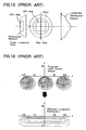
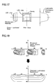
- the wavelength conversion element for car use by the present invention having a shape as schematically illustrated in FIG.17, shows higher luminosity over the whole chip, which means light flux is concentrated in a small area, when compared with the conventional chip illustrated in FIG.15. Consequently, a more distinctive cut-off is attained by the present invention as illustrated in FIG.18 compared with that of the conventional chip (see FIG.16).
- FIGs.3A and 3B The present embodiment is explained as referring to FIGs.3A and 3B.
- FIGs.3A and 3B are schematic views illustrating the constitution of the wavelength conversion element which is applied to the LED lamp for car use.
- FIG.3A is the cross-sectional side view and
- FIG.3B is the plan view.
- An LED device constituted by layered GaN films being grown on a SiC substrate is manufactured as a chip T 1 .
- the chip T 1 has an area of 1 mm by 2mm and a height of 0.3mm and emits excitation light with a wavelength of 470nm.
- the flip chip type junction is selected for the present chip.
- the cavity E 1 of the chip T 1 illustrated in FIGs.3A and 3B by the present invention has a bottom of 1.1mm by 2.1 mm and an angle between the side surface of the cavity and the bottom is formed upright.
- FIGs.4A and 4B are schematic views illustrating the conventional chip.
- FIG.4A is the cross-sectional side view and
- FIG.4B is the plan view.
- a cavity Ex of the conventional chip has a circular bottom with a diameter of 3.0mm and a side surface with an inclined angle of 45 ⁇ .
- Performances of the lamps for car use constituted by the above-mentioned chips are compared. Performance data measured without attaching a lens to the lamp assembly are shown in TAB.1.
- Conventional LED (FIGs.4A, 4B)
- Embodiment 1 (FIGs.3A, 3B) Luminous Flux 36.4 Im 30.5 Im Area of Cavity Opening 12.6 mm 2 2.3 mm 2 Luminous Emittance 2.89 Im/mm 2 13.3 Im/mm 2
- the luminous emittance is improved when the more converging and smaller cavity E 1 is employed, so that embodiment 1 is judged to be an excellent wavelength conversion element for car use.
- LED devices constituted by layered GaN films being grown on SiC substrates are manufactured as chip T 2 illustrated in FIGs.5A and 5B, and T 3 illustrated in FIGs.6A and 6B.
- the chips T 2 and T 3 respectively have an area of 1 mm by 1 mm and a height of 0.3mm and emit excitation light with a wavelength of 470nm.
- the flip chip type junctions are selected for both chips.
- the side surface of the chip T 2 is formed upright and the whole side surfaces of the chip are inclined 45°in relation to the bottom of the chip T 3 .
- the cavity E ⁇ illustrated in FIGs.5A and 5B has a bottom of 1.1mm by 1.1 mm and the cavity E 3 illustrated in FIGs.6A and 6B has a bottom of 0.5mm by 0.5mm and a cavity opening of 1.1mm by 1. 1mm.
- a silicon resin mixed with a YAG:Ce fluorescent material is filled in a cavity E 2 of chip T 2 illustrated in FIGs.5A and 5B so as to obtain white light.
- N 2 gas is filled around the chip T 3 illustrated in FIGs.6A and 6B and a quartz glass plate coated with a solution including the same fluorescent material as the chip T 2 , employed as a wavelength conversion part F 1 , is applied to the upper portion of the chip T 3 such that the coated side of the quartz glass plate is closely contacted to the chip T 3 .
- FIGs.5A, 5B Upright sided chip
- FIGs.6A, 6B Inclined sided chip
- LED devices constituted by layered GaN films being grown on SiC substrates are manufactured as chip T 4 illustrated in FIGs.7A and 7B, and T 5 illustrated in FIGs.8A and 8B.
- the chips T 4 and T 5 respectively have an area of 1 mm by 2mm and a height of 0.3mm and emit excitation light with a wavelength of 470nm.
- the junction down type junctions are selected for both chips.
- the side surfaces of the cavities of the chip T 4 and T 5 are formed upright.
- Both cavities E 4 and E 4 respectively have a bottom of 1.1 mm by 2.1 mm.
- the light extracting part is not employed in the chip T 4 illustrated in FIGs.7A and 7B.
- a silicon resin mixed with a YAG:Ce fluorescent material is filled in both cavities E 4 and E 4 so as to obtain white light.
- An LED device constituted by layered GaN films being grown on a SiC substrate is manufactured as chip T 6 illustrated in FIGs.9A and 9B.
- the chip T 6 has an area of 1 mm by 1 mm and a height of 0.3mm and emit excitation light with a wavelength of 470nm.
- the junction down type junction is selected for the present chip.
- the side surface of the cavity of the chip T 6 is formed upright.
- a cavity E 5 has a bottom of 1.2mm by 1.2mm.
- the light extracting part is not arranged in the chip T 6 .
- a silicon resin mixed with a YAG:Ce fluorescent material is filled in the cavity E 5 so as to obtain white light.
- a Performance of the chip T 6 is measured without attaching a lens to the lamp assembly and obtained data is shown in TAB.4.
- Upright sided chip (FIGs.9A, 9B) Luminous Flux 16.1 Im Area of Cavity Opening 1.44 mm 2 Luminous Emittance 11.2 Im/mm 2 From data in TAB.4, it is confirmed that the enough luminous emittance is obtained even when the side surface of chip is not formed inclined.
- a light distribution pattern illustrated in FIG.10 is obtained by a simulation carried out in the following manner: a lamp assembly of a headlight for car use, which employs 16 chips illustrated in FIGs.9A and 9B and an optimized reflector, is supposed to irradiate a light beam ahead. From the light distribution pattern in FIG.10 it is confirmed that a clear cut off is realized when the present chips are employed in the lamp assembly.
- FIGs.11A and 11B is an example of LED lamps for car use in which chips are arranged.
- An LED device is arranged as a multi-type chip consisting of two chips T 7 mounted on a base. Each chip is constituted by layered GaN films being grown on a SiC substrate.
- the chip T 7 has an area of 0.9mm by 0.9mm and a height of 0.3mm and emit excitation light with a wavelength of 470nm.
- the junction down type junctions are selected for the present chips.
- the side surface of the cavity of the chip T 7 is formed upright.
- a cavity E 6 has a bottom of 1.1mm by 2.1 mm.
- Two chips T 7 are arranged in the cavity E 6 where distances between the chip T 7 and the side surface of the cavity E 6 , and a distance between two chips T 7 are arranged at 100 ⁇ m.
- a silicon resin mixed with a YAG:Ce fluorescent material is filled in the cavity E 6 so as to obtain white light.
- a performance of the LED device illustrated in FIGs.11A and 11B is measured without attaching a lens to the lamp assembly and obtained data is shown in TAB.5.
- Multi-type chip (FIGs.11A, 11B) Luminous Flux 28.2 Im Area of Cavity Opening 2.3 mm 2 Luminous Emittance 12.3 Im/mm 2 From data in TAB.5, it is confirmed that the enough luminous emittance is obtained by employing the multi-type chip.
- the LED device can be employed as a light source of the headlight for car use, since the enough luminous emittance and a light intensity for the headlight is realized by employing a plurality of LED devices.
- the present invention can provide chips as practical products employable in LED headlights and LED fog lamps. Since some of the side surfaces of the chips and the cavities by the present invention are formed in a straight line, a headlight of a car can be formed such that irradiated light from the headlight is prevented from reaching to a driver in the opposite lane.
- the area of the cavity opening is set less than two times of the maximum area of the light emitting part, a sufficient luminous flux diverging rate can be obtained.
- the angle ⁇ 2 between the bottom of the cavity and the side surface of the cavity can be set in a range of more than 0°and less than 90°, various types of LED devices for car use can be provided.
- the base of the LED device by the present invention has at least one straight portion, the LED device as a light source is attached to the lamp assembly by its strait portion, the cavity is not fitted at a wrong angle to the lamp assembly. Therefore the straight portion of the base has an effect to prevent from obtaining an undesired light distribution pattern due to a deviation in the attached angle of the base of the LED device to the lamp assembly.
Landscapes
- Non-Portable Lighting Devices Or Systems Thereof (AREA)
- Led Device Packages (AREA)
- Led Devices (AREA)
Applications Claiming Priority (2)
| Application Number | Priority Date | Filing Date | Title |
|---|---|---|---|
| JP2002301931 | 2002-10-16 | ||
| JP2002301931A JP4143732B2 (ja) | 2002-10-16 | 2002-10-16 | 車載用波長変換素子 |
Publications (3)
| Publication Number | Publication Date |
|---|---|
| EP1411557A2 true EP1411557A2 (fr) | 2004-04-21 |
| EP1411557A3 EP1411557A3 (fr) | 2007-05-23 |
| EP1411557B1 EP1411557B1 (fr) | 2014-05-07 |
Family
ID=32040815
Family Applications (1)
| Application Number | Title | Priority Date | Filing Date |
|---|---|---|---|
| EP03022027.1A Expired - Lifetime EP1411557B1 (fr) | 2002-10-16 | 2003-10-01 | LED avec convertisseur de longueur d'onde optique destiné à être utilisé dans une voiture |
Country Status (4)
| Country | Link |
|---|---|
| US (1) | US6855958B2 (fr) |
| EP (1) | EP1411557B1 (fr) |
| JP (1) | JP4143732B2 (fr) |
| CN (1) | CN100380689C (fr) |
Cited By (18)
| Publication number | Priority date | Publication date | Assignee | Title |
|---|---|---|---|---|
| WO2006048064A1 (fr) | 2004-11-03 | 2006-05-11 | Tridonic Optoelectronics Gmbh | Ensemble diode electroluminescente pourvue d'une matiere de conversion de couleur |
| DE102006015788A1 (de) * | 2006-01-27 | 2007-09-13 | Osram Opto Semiconductors Gmbh | Optoelektronischer Halbleiterchip |
| DE102006046199A1 (de) * | 2006-09-29 | 2008-04-03 | Osram Opto Semiconductors Gmbh | Optoelektronisches Bauelement |
| EP1663706A4 (fr) * | 2003-09-08 | 2008-11-05 | Odelo Gmbh | Source lumineuse del |
| EP1988583A1 (fr) * | 2007-04-30 | 2008-11-05 | TridonicAtco Optoelectronics GMBH | Module DEL doté d'une couche de conversion de couleur conçue pour une distribution homogène des couleurs |
| WO2010027649A1 (fr) * | 2008-09-04 | 2010-03-11 | 3M Innovative Properties Company | Source de lumière monochromatique à rapport d'aspect élevé |
| WO2010027650A1 (fr) * | 2008-09-04 | 2010-03-11 | 3M Innovative Properties Company | Source de lumière à monochromaticité améliorée |
| EP1887637A3 (fr) * | 2006-08-08 | 2010-09-15 | LG Electronics Inc. | Paquet de dispositif électroluminescent et son procédé de fabrication |
| EP1670074A3 (fr) * | 2004-12-08 | 2010-11-17 | Sumitomo Electric Industries, Ltd. | Phare à diodes électroluminescentes |
| EP1672704A3 (fr) * | 2004-12-20 | 2010-11-17 | Sumitomo Electric Industries, Ltd. | Diode électroluminescente |
| EP2246913A3 (fr) * | 2009-04-28 | 2011-07-20 | LG Innotek Co., Ltd. | Conditionnement de dispositif électroluminescent et système d'éclairage l'incluant |
| US8385380B2 (en) | 2008-09-04 | 2013-02-26 | 3M Innovative Properties Company | Monochromatic light source |
| US8488641B2 (en) | 2008-09-04 | 2013-07-16 | 3M Innovative Properties Company | II-VI MQW VSEL on a heat sink optically pumped by a GaN LD |
| TWI455350B (zh) * | 2008-04-29 | 2014-10-01 | Schott Ag | 特別用於含發光二極體的白或彩色光源之轉換材料及其製法和含此轉換材料的光源 |
| WO2014167455A3 (fr) * | 2013-04-11 | 2015-01-08 | Koninklijke Philips N.V. | Dispositif d'émission de lumière à semi-conducteurs émettant par le haut |
| WO2015101854A1 (fr) * | 2014-01-06 | 2015-07-09 | Koninklijke Philips N.V. | Dispositif électroluminescent à semi-conducteur comportant un substrat formé et son procédé de fabrication |
| EP2736087A3 (fr) * | 2012-11-22 | 2016-03-09 | Kabushiki Kaisha Toshiba | Dispositif électroluminescent semi-conducteur et son procédé de fabrication |
| WO2018125985A1 (fr) * | 2016-12-30 | 2018-07-05 | Lumileds Llc | Boîtier de del utilisant l'impression par stencil électro-formé |
Families Citing this family (40)
| Publication number | Priority date | Publication date | Assignee | Title |
|---|---|---|---|---|
| JP4143732B2 (ja) * | 2002-10-16 | 2008-09-03 | スタンレー電気株式会社 | 車載用波長変換素子 |
| JP2004304161A (ja) * | 2003-03-14 | 2004-10-28 | Sony Corp | 発光素子、発光装置、画像表示装置、発光素子の製造方法及び画像表示装置の製造方法 |
| JP4138586B2 (ja) * | 2003-06-13 | 2008-08-27 | スタンレー電気株式会社 | 光源用ledランプおよびこれを用いた車両用前照灯 |
| JP4314911B2 (ja) * | 2003-08-20 | 2009-08-19 | スタンレー電気株式会社 | 車両前照灯 |
| JP4140042B2 (ja) * | 2003-09-17 | 2008-08-27 | スタンレー電気株式会社 | 蛍光体を用いたled光源装置及びled光源装置を用いた車両前照灯 |
| JP4402425B2 (ja) * | 2003-10-24 | 2010-01-20 | スタンレー電気株式会社 | 車両前照灯 |
| CN100505336C (zh) * | 2004-07-29 | 2009-06-24 | 晶元光电股份有限公司 | 具有微反射器的倒装芯片式发光元件 |
| JP4599111B2 (ja) * | 2004-07-30 | 2010-12-15 | スタンレー電気株式会社 | 灯具光源用ledランプ |
| ES2515865T3 (es) * | 2004-09-20 | 2014-10-30 | Koninklijke Philips N.V. | Elemento colimador de LED con un reflector semiparabólico |
| EP1794491B1 (fr) * | 2004-09-20 | 2011-06-29 | Philips Intellectual Property & Standards GmbH | Element collimateur a diode del ayant un collimateur asymetrique |
| KR100667508B1 (ko) * | 2004-11-08 | 2007-01-10 | 엘지전자 주식회사 | 발광 소자 및 그의 제조방법 |
| EP1815287A1 (fr) * | 2004-11-18 | 2007-08-08 | Koninklijke Philips Electronics N.V. | Systeme d'eclairage et projecteur de vehicule |
| JP4992282B2 (ja) * | 2005-06-10 | 2012-08-08 | ソニー株式会社 | 発光ダイオード、発光ダイオードの製造方法、発光ダイオードバックライト、発光ダイオード照明装置、発光ダイオードディスプレイおよび電子機器 |
| KR100606551B1 (ko) * | 2005-07-05 | 2006-08-01 | 엘지전자 주식회사 | 발광소자 제조방법 |
| KR100682877B1 (ko) * | 2005-07-12 | 2007-02-15 | 삼성전기주식회사 | 발광다이오드 및 그 제조방법 |
| CN101326400B (zh) * | 2005-12-12 | 2011-02-23 | 皇家飞利浦电子股份有限公司 | 用于具有低光束功能的车辆前灯的发光二极管准直仪元件 |
| US8044412B2 (en) | 2006-01-20 | 2011-10-25 | Taiwan Semiconductor Manufacturing Company, Ltd | Package for a light emitting element |
| KR20070093271A (ko) * | 2006-03-13 | 2007-09-18 | 엘지이노텍 주식회사 | 질화물 반도체 발광소자 및 그 제조 방법 |
| JP4729441B2 (ja) | 2006-06-09 | 2011-07-20 | スタンレー電気株式会社 | 車両用灯具 |
| JP4725456B2 (ja) * | 2006-08-09 | 2011-07-13 | セイコーエプソン株式会社 | 固体光源およびプロジェクタ |
| JP4535053B2 (ja) * | 2006-10-12 | 2010-09-01 | ソニー株式会社 | 発光ダイオードの配線の形成方法、発光ダイオード実装基板、ディスプレイ、バックライト、照明装置および電子機器 |
| JP4895831B2 (ja) | 2007-01-18 | 2012-03-14 | スタンレー電気株式会社 | 車両用灯具 |
| JP4290745B2 (ja) * | 2007-03-16 | 2009-07-08 | 豊田合成株式会社 | Iii−v族半導体素子の製造方法 |
| US8143777B2 (en) | 2007-08-23 | 2012-03-27 | Stanley Electric Co., Ltd. | LED lighting unit with LEDs and phosphor materials |
| JP5152502B2 (ja) * | 2008-06-09 | 2013-02-27 | スタンレー電気株式会社 | 灯具 |
| JP5340879B2 (ja) | 2009-10-13 | 2013-11-13 | スタンレー電気株式会社 | 発光装置 |
| CN102054905A (zh) * | 2009-10-29 | 2011-05-11 | 展晶科技(深圳)有限公司 | 具有导热层的发光二极管芯片 |
| JP5571419B2 (ja) | 2010-03-24 | 2014-08-13 | スタンレー電気株式会社 | 車両用前照灯 |
| JP4945658B2 (ja) * | 2010-05-17 | 2012-06-06 | スタンレー電気株式会社 | 車両用前照灯 |
| US9070851B2 (en) | 2010-09-24 | 2015-06-30 | Seoul Semiconductor Co., Ltd. | Wafer-level light emitting diode package and method of fabricating the same |
| KR101142965B1 (ko) * | 2010-09-24 | 2012-05-08 | 서울반도체 주식회사 | 웨이퍼 레벨 발광 다이오드 패키지 및 그것을 제조하는 방법 |
| JP2012243701A (ja) * | 2011-05-24 | 2012-12-10 | Stanley Electric Co Ltd | 光源装置および照明装置 |
| CN108565329A (zh) * | 2011-11-17 | 2018-09-21 | 株式会社流明斯 | 发光元件封装体以及包括该发光元件封装体的背光单元 |
| CN110265530B (zh) * | 2014-01-29 | 2023-03-21 | 亮锐控股有限公司 | 填充有密封剂的用于磷光体转换led的浅反射器杯 |
| WO2015138495A1 (fr) * | 2014-03-11 | 2015-09-17 | Osram Sylvania Inc. | Ensembles convertisseurs optiques à dissipation thermique améliorée |
| JP2016076634A (ja) * | 2014-10-08 | 2016-05-12 | エルジー ディスプレイ カンパニー リミテッド | Ledパッケージ、バックライトユニット及び液晶表示装置 |
| CN106505136A (zh) * | 2015-09-07 | 2017-03-15 | 包建敏 | 一种石英玻璃衬底led深紫外倒装芯片 |
| CN205944139U (zh) | 2016-03-30 | 2017-02-08 | 首尔伟傲世有限公司 | 紫外线发光二极管封装件以及包含此的发光二极管模块 |
| JP7221659B2 (ja) * | 2017-11-17 | 2023-02-14 | スタンレー電気株式会社 | 半導体発光装置 |
| CN111480033A (zh) * | 2017-12-15 | 2020-07-31 | 昕诺飞控股有限公司 | 照明设备壳体、灯具以及制造方法 |
Citations (5)
| Publication number | Priority date | Publication date | Assignee | Title |
|---|---|---|---|---|
| US3780357A (en) | 1973-02-16 | 1973-12-18 | Hewlett Packard Co | Electroluminescent semiconductor display apparatus and method of fabricating the same |
| JPH10107325A (ja) | 1996-09-30 | 1998-04-24 | Nichia Chem Ind Ltd | 発光装置及びそれを用いた表示装置 |
| DE19747433A1 (de) | 1997-10-28 | 1999-05-06 | Vishay Semiconductor Gmbh | Lichtemittierende Halbleiterdiode |
| US6121635A (en) | 1997-04-15 | 2000-09-19 | Kabushiki Kaisha Toshiba | Semiconductor light-emitting element having transparent electrode and current blocking layer, and semiconductor light-emitting including the same |
| EP1041650A2 (fr) | 1999-03-31 | 2000-10-04 | Toyoda Gosei Co., Ltd. | Dispositif semi-conducteur émetteur de lumière comprenant un composé nitride III-V |
Family Cites Families (11)
| Publication number | Priority date | Publication date | Assignee | Title |
|---|---|---|---|---|
| US5055892A (en) * | 1989-08-29 | 1991-10-08 | Hewlett-Packard Company | High efficiency lamp or light accepter |
| JPH0799345A (ja) * | 1993-09-28 | 1995-04-11 | Nichia Chem Ind Ltd | 発光ダイオード |
| JPH07211943A (ja) * | 1994-01-25 | 1995-08-11 | Nikon Corp | 光源装置 |
| EP0905797B1 (fr) * | 1997-09-29 | 2010-02-10 | OSRAM Opto Semiconductors GmbH | Source lumineuse à semi-conducteur et méthode de fabricaton |
| JPH11135507A (ja) * | 1997-10-29 | 1999-05-21 | Sharp Corp | 導電層の形成方法および液晶表示装置の製造方法 |
| US6404125B1 (en) * | 1998-10-21 | 2002-06-11 | Sarnoff Corporation | Method and apparatus for performing wavelength-conversion using phosphors with light emitting diodes |
| US6329676B1 (en) * | 1999-03-01 | 2001-12-11 | Toru Takayama | Flat panel solid state light source |
| DE19918370B4 (de) * | 1999-04-22 | 2006-06-08 | Osram Opto Semiconductors Gmbh | LED-Weißlichtquelle mit Linse |
| US6559594B2 (en) * | 2000-02-03 | 2003-05-06 | Semiconductor Energy Laboratory Co., Ltd. | Light-emitting device |
| US6455878B1 (en) * | 2001-05-15 | 2002-09-24 | Lumileds Lighting U.S., Llc | Semiconductor LED flip-chip having low refractive index underfill |
| JP4143732B2 (ja) * | 2002-10-16 | 2008-09-03 | スタンレー電気株式会社 | 車載用波長変換素子 |
-
2002
- 2002-10-16 JP JP2002301931A patent/JP4143732B2/ja not_active Expired - Fee Related
-
2003
- 2003-10-01 EP EP03022027.1A patent/EP1411557B1/fr not_active Expired - Lifetime
- 2003-10-09 US US10/682,697 patent/US6855958B2/en not_active Expired - Lifetime
- 2003-10-15 CN CNB2003101013373A patent/CN100380689C/zh not_active Expired - Fee Related
Patent Citations (5)
| Publication number | Priority date | Publication date | Assignee | Title |
|---|---|---|---|---|
| US3780357A (en) | 1973-02-16 | 1973-12-18 | Hewlett Packard Co | Electroluminescent semiconductor display apparatus and method of fabricating the same |
| JPH10107325A (ja) | 1996-09-30 | 1998-04-24 | Nichia Chem Ind Ltd | 発光装置及びそれを用いた表示装置 |
| US6121635A (en) | 1997-04-15 | 2000-09-19 | Kabushiki Kaisha Toshiba | Semiconductor light-emitting element having transparent electrode and current blocking layer, and semiconductor light-emitting including the same |
| DE19747433A1 (de) | 1997-10-28 | 1999-05-06 | Vishay Semiconductor Gmbh | Lichtemittierende Halbleiterdiode |
| EP1041650A2 (fr) | 1999-03-31 | 2000-10-04 | Toyoda Gosei Co., Ltd. | Dispositif semi-conducteur émetteur de lumière comprenant un composé nitride III-V |
Cited By (32)
| Publication number | Priority date | Publication date | Assignee | Title |
|---|---|---|---|---|
| EP1663706A4 (fr) * | 2003-09-08 | 2008-11-05 | Odelo Gmbh | Source lumineuse del |
| US7777236B2 (en) | 2004-11-03 | 2010-08-17 | Tridonic Optoelectronics Gmbh | Light-emitting diode arrangement comprising a color-converting material |
| WO2006048064A1 (fr) | 2004-11-03 | 2006-05-11 | Tridonic Optoelectronics Gmbh | Ensemble diode electroluminescente pourvue d'une matiere de conversion de couleur |
| EP1670074A3 (fr) * | 2004-12-08 | 2010-11-17 | Sumitomo Electric Industries, Ltd. | Phare à diodes électroluminescentes |
| EP1672704A3 (fr) * | 2004-12-20 | 2010-11-17 | Sumitomo Electric Industries, Ltd. | Diode électroluminescente |
| DE102006015788A1 (de) * | 2006-01-27 | 2007-09-13 | Osram Opto Semiconductors Gmbh | Optoelektronischer Halbleiterchip |
| US8581280B2 (en) | 2006-01-27 | 2013-11-12 | Osram Opto Semiconductors Gmbh | Optoelectronic semiconductor chip |
| US9166123B2 (en) | 2006-08-08 | 2015-10-20 | Lg Electronics Inc. | Light emitting device package and method for manufacturing the same |
| EP1887637A3 (fr) * | 2006-08-08 | 2010-09-15 | LG Electronics Inc. | Paquet de dispositif électroluminescent et son procédé de fabrication |
| US8093610B2 (en) | 2006-09-29 | 2012-01-10 | Osram Opto Semiconductors Gmbh | Optoelectronic component |
| DE102006046199A1 (de) * | 2006-09-29 | 2008-04-03 | Osram Opto Semiconductors Gmbh | Optoelektronisches Bauelement |
| WO2008131877A1 (fr) * | 2007-04-30 | 2008-11-06 | Ledon Lighting Jennersdorf Gmbh | Module de del avec couche de conversion de couleur conçue pour une distribution de couleur homogène |
| EP1988583A1 (fr) * | 2007-04-30 | 2008-11-05 | TridonicAtco Optoelectronics GMBH | Module DEL doté d'une couche de conversion de couleur conçue pour une distribution homogène des couleurs |
| US8309981B2 (en) | 2007-04-30 | 2012-11-13 | Ledon Lighting Jennersdorf Gmbh | LED module with color conversion layer designed for a homogenous color distribution |
| US9950949B2 (en) | 2008-04-29 | 2018-04-24 | Schott Ag | Conversion material, particularly for a white or colored light souce comprising a semiconductor light source, a method for the production thereof, as well as a light source comprising said conversion material |
| US10988408B2 (en) | 2008-04-29 | 2021-04-27 | Schott Ag | Conversion material for white or colored light source, method of production, and light source having the conversion material |
| TWI455350B (zh) * | 2008-04-29 | 2014-10-01 | Schott Ag | 特別用於含發光二極體的白或彩色光源之轉換材料及其製法和含此轉換材料的光源 |
| US8385380B2 (en) | 2008-09-04 | 2013-02-26 | 3M Innovative Properties Company | Monochromatic light source |
| WO2010027649A1 (fr) * | 2008-09-04 | 2010-03-11 | 3M Innovative Properties Company | Source de lumière monochromatique à rapport d'aspect élevé |
| US8193543B2 (en) | 2008-09-04 | 2012-06-05 | 3M Innovative Properties Company | Monochromatic light source with high aspect ratio |
| US8488641B2 (en) | 2008-09-04 | 2013-07-16 | 3M Innovative Properties Company | II-VI MQW VSEL on a heat sink optically pumped by a GaN LD |
| WO2010027650A1 (fr) * | 2008-09-04 | 2010-03-11 | 3M Innovative Properties Company | Source de lumière à monochromaticité améliorée |
| EP2246913A3 (fr) * | 2009-04-28 | 2011-07-20 | LG Innotek Co., Ltd. | Conditionnement de dispositif électroluminescent et système d'éclairage l'incluant |
| US9401467B2 (en) | 2009-04-28 | 2016-07-26 | Lg Innotek Co., Ltd. | Light emitting device package having a package body including a recess and lighting system including the same |
| EP2736087A3 (fr) * | 2012-11-22 | 2016-03-09 | Kabushiki Kaisha Toshiba | Dispositif électroluminescent semi-conducteur et son procédé de fabrication |
| WO2014167455A3 (fr) * | 2013-04-11 | 2015-01-08 | Koninklijke Philips N.V. | Dispositif d'émission de lumière à semi-conducteurs émettant par le haut |
| US9871167B2 (en) | 2013-04-11 | 2018-01-16 | Koninklijke Philips N.V. | Top emitting semiconductor light emitting device |
| WO2015101854A1 (fr) * | 2014-01-06 | 2015-07-09 | Koninklijke Philips N.V. | Dispositif électroluminescent à semi-conducteur comportant un substrat formé et son procédé de fabrication |
| US10090436B2 (en) | 2014-01-06 | 2018-10-02 | Lumileds Llc | Semiconductor light emitting device with shaped substrate and method of manufacturing the same |
| US10686109B2 (en) | 2016-12-30 | 2020-06-16 | Lumileds Llc | LED package using electroform stencil printing |
| US10916689B2 (en) | 2016-12-30 | 2021-02-09 | Lumileds Llc | LED package using electroform stencil printing |
| WO2018125985A1 (fr) * | 2016-12-30 | 2018-07-05 | Lumileds Llc | Boîtier de del utilisant l'impression par stencil électro-formé |
Also Published As
| Publication number | Publication date |
|---|---|
| CN1497745A (zh) | 2004-05-19 |
| EP1411557A3 (fr) | 2007-05-23 |
| EP1411557B1 (fr) | 2014-05-07 |
| JP2004140090A (ja) | 2004-05-13 |
| CN100380689C (zh) | 2008-04-09 |
| JP4143732B2 (ja) | 2008-09-03 |
| US6855958B2 (en) | 2005-02-15 |
| US20040076016A1 (en) | 2004-04-22 |
Similar Documents
| Publication | Publication Date | Title |
|---|---|---|
| US6855958B2 (en) | Wavelength conversion element for car use | |
| JP3228571U (ja) | レーザー装置のパッケージ構造 | |
| CN100570205C (zh) | 车辆前照灯用光源装置和车辆前照灯 | |
| US6945672B2 (en) | LED planar light source and low-profile headlight constructed therewith | |
| US7520647B2 (en) | Light source and vehicle lamp | |
| US9726340B2 (en) | Semiconductor light-emitting apparatus and vehicle headlight | |
| CN103392093B (zh) | 发光模块及车辆用灯具 | |
| US8258527B2 (en) | Lighting device and semiconductor light source device | |
| JP2005093191A5 (fr) | ||
| US7566152B2 (en) | Vehicular lamp unit | |
| JP2006237264A (ja) | 発光装置および照明装置 | |
| US7422349B2 (en) | Led lighting apparatus | |
| CN207250931U (zh) | 一种导光结构 | |
| US8568007B2 (en) | Vehicle headlight | |
| KR102412984B1 (ko) | 컵들 내의 광 추출 브리지 | |
| EP1857729A1 (fr) | Module optoelectronique et système d'illumination avec un tel module | |
| CN110710069A (zh) | 一种激光器封装结构 | |
| JP2007150255A (ja) | 発光ダイオード照明モジュールおよび照明装置 | |
| CN101803047A (zh) | 准直器 | |
| CN119905494A (zh) | 发光装置和发光装置的制备方法 |
Legal Events
| Date | Code | Title | Description |
|---|---|---|---|
| PUAI | Public reference made under article 153(3) epc to a published international application that has entered the european phase |
Free format text: ORIGINAL CODE: 0009012 |
|
| AK | Designated contracting states |
Kind code of ref document: A2 Designated state(s): AT BE BG CH CY CZ DE DK EE ES FI FR GB GR HU IE IT LI LU MC NL PT RO SE SI SK TR |
|
| AX | Request for extension of the european patent |
Extension state: AL LT LV MK |
|
| PUAL | Search report despatched |
Free format text: ORIGINAL CODE: 0009013 |
|
| AK | Designated contracting states |
Kind code of ref document: A3 Designated state(s): AT BE BG CH CY CZ DE DK EE ES FI FR GB GR HU IE IT LI LU MC NL PT RO SE SI SK TR |
|
| AX | Request for extension of the european patent |
Extension state: AL LT LV MK |
|
| 17P | Request for examination filed |
Effective date: 20071123 |
|
| AKX | Designation fees paid |
Designated state(s): DE FR GB HU IT NL |
|
| 17Q | First examination report despatched |
Effective date: 20091015 |
|
| REG | Reference to a national code |
Ref country code: DE Ref legal event code: R079 Ref document number: 60346116 Country of ref document: DE Free format text: PREVIOUS MAIN CLASS: H01L0033000000 Ipc: H01L0033200000 |
|
| RIC1 | Information provided on ipc code assigned before grant |
Ipc: H01L 33/20 20100101AFI20130916BHEP Ipc: H01L 33/60 20100101ALI20130916BHEP |
|
| GRAP | Despatch of communication of intention to grant a patent |
Free format text: ORIGINAL CODE: EPIDOSNIGR1 |
|
| INTG | Intention to grant announced |
Effective date: 20131113 |
|
| GRAS | Grant fee paid |
Free format text: ORIGINAL CODE: EPIDOSNIGR3 |
|
| GRAA | (expected) grant |
Free format text: ORIGINAL CODE: 0009210 |
|
| AK | Designated contracting states |
Kind code of ref document: B1 Designated state(s): DE FR GB HU IT NL |
|
| REG | Reference to a national code |
Ref country code: GB Ref legal event code: FG4D |
|
| REG | Reference to a national code |
Ref country code: DE Ref legal event code: R096 Ref document number: 60346116 Country of ref document: DE Effective date: 20140618 |
|
| REG | Reference to a national code |
Ref country code: NL Ref legal event code: VDEP Effective date: 20140507 |
|
| REG | Reference to a national code |
Ref country code: DE Ref legal event code: R097 Ref document number: 60346116 Country of ref document: DE |
|
| PG25 | Lapsed in a contracting state [announced via postgrant information from national office to epo] |
Ref country code: NL Free format text: LAPSE BECAUSE OF FAILURE TO SUBMIT A TRANSLATION OF THE DESCRIPTION OR TO PAY THE FEE WITHIN THE PRESCRIBED TIME-LIMIT Effective date: 20140507 |
|
| PLBE | No opposition filed within time limit |
Free format text: ORIGINAL CODE: 0009261 |
|
| STAA | Information on the status of an ep patent application or granted ep patent |
Free format text: STATUS: NO OPPOSITION FILED WITHIN TIME LIMIT |
|
| 26N | No opposition filed |
Effective date: 20150210 |
|
| PG25 | Lapsed in a contracting state [announced via postgrant information from national office to epo] |
Ref country code: IT Free format text: LAPSE BECAUSE OF FAILURE TO SUBMIT A TRANSLATION OF THE DESCRIPTION OR TO PAY THE FEE WITHIN THE PRESCRIBED TIME-LIMIT Effective date: 20140507 |
|
| REG | Reference to a national code |
Ref country code: DE Ref legal event code: R097 Ref document number: 60346116 Country of ref document: DE Effective date: 20150210 |
|
| PG25 | Lapsed in a contracting state [announced via postgrant information from national office to epo] |
Ref country code: HU Free format text: LAPSE BECAUSE OF FAILURE TO SUBMIT A TRANSLATION OF THE DESCRIPTION OR TO PAY THE FEE WITHIN THE PRESCRIBED TIME-LIMIT; INVALID AB INITIO Effective date: 20031001 |
|
| REG | Reference to a national code |
Ref country code: FR Ref legal event code: PLFP Year of fee payment: 14 |
|
| REG | Reference to a national code |
Ref country code: FR Ref legal event code: PLFP Year of fee payment: 15 |
|
| REG | Reference to a national code |
Ref country code: FR Ref legal event code: PLFP Year of fee payment: 16 |
|
| PGFP | Annual fee paid to national office [announced via postgrant information from national office to epo] |
Ref country code: GB Payment date: 20200925 Year of fee payment: 18 Ref country code: FR Payment date: 20200914 Year of fee payment: 18 |
|
| PGFP | Annual fee paid to national office [announced via postgrant information from national office to epo] |
Ref country code: DE Payment date: 20200916 Year of fee payment: 18 |
|
| REG | Reference to a national code |
Ref country code: DE Ref legal event code: R119 Ref document number: 60346116 Country of ref document: DE |
|
| GBPC | Gb: european patent ceased through non-payment of renewal fee |
Effective date: 20211001 |
|
| PG25 | Lapsed in a contracting state [announced via postgrant information from national office to epo] |
Ref country code: GB Free format text: LAPSE BECAUSE OF NON-PAYMENT OF DUE FEES Effective date: 20211001 Ref country code: DE Free format text: LAPSE BECAUSE OF NON-PAYMENT OF DUE FEES Effective date: 20220503 |
|
| PG25 | Lapsed in a contracting state [announced via postgrant information from national office to epo] |
Ref country code: FR Free format text: LAPSE BECAUSE OF NON-PAYMENT OF DUE FEES Effective date: 20211031 |