EP1414071A2 - Procédé de fabrication d'un capteur d'image avec des microlentilles en forme concave - Google Patents
Procédé de fabrication d'un capteur d'image avec des microlentilles en forme concave Download PDFInfo
- Publication number
- EP1414071A2 EP1414071A2 EP03256674A EP03256674A EP1414071A2 EP 1414071 A2 EP1414071 A2 EP 1414071A2 EP 03256674 A EP03256674 A EP 03256674A EP 03256674 A EP03256674 A EP 03256674A EP 1414071 A2 EP1414071 A2 EP 1414071A2
- Authority
- EP
- European Patent Office
- Prior art keywords
- micro
- forming
- base material
- lens
- light sensitive
- Prior art date
- Legal status (The legal status is an assumption and is not a legal conclusion. Google has not performed a legal analysis and makes no representation as to the accuracy of the status listed.)
- Withdrawn
Links
Images


Classifications
-
- H—ELECTRICITY
- H10—SEMICONDUCTOR DEVICES; ELECTRIC SOLID-STATE DEVICES NOT OTHERWISE PROVIDED FOR
- H10F—INORGANIC SEMICONDUCTOR DEVICES SENSITIVE TO INFRARED RADIATION, LIGHT, ELECTROMAGNETIC RADIATION OF SHORTER WAVELENGTH OR CORPUSCULAR RADIATION
- H10F39/00—Integrated devices, or assemblies of multiple devices, comprising at least one element covered by group H10F30/00, e.g. radiation detectors comprising photodiode arrays
- H10F39/011—Manufacture or treatment of image sensors covered by group H10F39/12
- H10F39/024—Manufacture or treatment of image sensors covered by group H10F39/12 of coatings or optical elements
-
- H—ELECTRICITY
- H10—SEMICONDUCTOR DEVICES; ELECTRIC SOLID-STATE DEVICES NOT OTHERWISE PROVIDED FOR
- H10F—INORGANIC SEMICONDUCTOR DEVICES SENSITIVE TO INFRARED RADIATION, LIGHT, ELECTROMAGNETIC RADIATION OF SHORTER WAVELENGTH OR CORPUSCULAR RADIATION
- H10F39/00—Integrated devices, or assemblies of multiple devices, comprising at least one element covered by group H10F30/00, e.g. radiation detectors comprising photodiode arrays
- H10F39/80—Constructional details of image sensors
- H10F39/805—Coatings
- H10F39/8053—Colour filters
-
- H—ELECTRICITY
- H10—SEMICONDUCTOR DEVICES; ELECTRIC SOLID-STATE DEVICES NOT OTHERWISE PROVIDED FOR
- H10F—INORGANIC SEMICONDUCTOR DEVICES SENSITIVE TO INFRARED RADIATION, LIGHT, ELECTROMAGNETIC RADIATION OF SHORTER WAVELENGTH OR CORPUSCULAR RADIATION
- H10F39/00—Integrated devices, or assemblies of multiple devices, comprising at least one element covered by group H10F30/00, e.g. radiation detectors comprising photodiode arrays
- H10F39/80—Constructional details of image sensors
- H10F39/806—Optical elements or arrangements associated with the image sensors
- H10F39/8063—Microlenses
Definitions
- the present invention relates to image sensors, and more particularly, towards a method for manufacturing an image sensor that has a concave-shaped micro-lens.
- Image sensors are electronic integrated circuits that can be used to produce still or video images.
- Solid state image sensors can be either of the charge coupled device (CCD) type or the complimentary metal oxide semiconductor (CMOS) type. In either type of image sensor, a light gathering pixel is formed in a substrate and arranged in a two-dimensional array.
- Modern image sensors typically contain millions of pixels to provide a high resolution image.
- An important part of the image sensor are the color filters and micro-lens structures formed atop of the pixels.
- the color filters as the name implies, are operative, in conjunction with signal processing, to provide a color image.
- the micro-lenses serve to focus the incident light onto the pixels, and thus to improve the fill factor of each pixel.
- micro-lenses are formed by spin coating a layer of micro-lens material onto a planarized layer.
- the micro-lens material is then etched to form cylindrical or other shaped regions that are centered above each pixel. Then, the micro-lens material is heated and reflowed to form a convex hemispherical micro-lens.
- Figure 1 shows a prior art cross-sectional simplified diagram of an image sensor 101 having micro-lenses formed thereon.
- the image sensor includes a plurality of pixels that have light detecting elements 103 formed in the substrate.
- the light detecting elements 103 may be one of several types, such as a photodiode, a photogate, or other solid state light sensitive element.
- micro-lens 105 Formed atop of each pixel is a micro-lens 105.
- the micro-lens 105 focuses incident light onto the light detecting elements 103.
- various intervening layers that would typically include the color filter layers and various metal conducting lines.
- the present invention provides a method for forming an image sensor according to Claim 1.
- the present invention relates to a method for forming a concave micro-lens structure for use with image sensors, either of the CMOS or CCD type.
- image sensors either of the CMOS or CCD type.
- numerous specific details are provided to provide a thorough understanding of the embodiments of the invention.
- One skilled in the relevant art will recognize, however, that the invention can be practiced without one or more of the specific details, or with other methods, components, etc.
- well-known structures or operations are not shown or described in detail to avoid obscuring aspects of various embodiments of the invention.
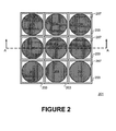
- Figure 2 shows a top view of an image sensor 201 formed in accordance with the present invention.
- the image sensor 201 includes a plurality of pixels 203 typically arranged in a two dimensional array.
- the image sensor shows a three by three array of pixels 203, though it can be appreciated that an actual mage sensor 201 would have many more pixels, arranged in more than perhaps a thousand rows and/or a thousand columns.
- Figure 2 shows the pixels in ordered columns and rows, the pixels may be arranged in any type of ordered arrangement. For example, alternating rows may have their pixels slightly offset from each other laterally in a checkerboard format.
- the pixels 203 typically include a light sensitive element, such as a photodiode or a photogate as two examples. However, it can be appreciated that other types of light sensitive elements, now known or developed in the future, may be used. Further, the pixels 203 will also include amplification and/or readout circuitry. For clarity, this circuitry is not shown in Figure 2. In one embodiment, the pixels 203 may be active pixels, commonly known in the prior art.
- micro-lens 205 Formed atop of each pixel 203 is a micro-lens 205.
- the micro-lens 205 is concave in nature, in contrast to the prior art convex micro-lens. Because of the nature of the concave micro-lenses 205, little or no gap exists between adjacent micro-lenses of adjacent pixels.
- the color filter 207 may be placed either between the micro-lens 205 and the light sensitive element, or alternatively, be formed atop of the micro-lens 205.
- the color filter 207 is typically a pigmented or dyed material that will only allow a narrow band of light to pass therethrough, for example, red, blue, or green. In other embodiments, the color filter may be cyan, yellow, or magenta. These are but example colors for the color filters 207 and the present invention is meant to encompass a color filter 207 having any color. While the use of pigmented or dyed color materials is the most prevalent form of color filters, other reflective type color filters may be used, such as a multilayer stack reflective material.
- color filters 207 are known in art and will not be described herein to avoid any unnecessary obscuration with the description of the present invention.
- U.S. Patent No. 6,297,071, U.S. Patent No. 6,362,513, and U.S. Patent No. 6,271,900 show the current state of the color filter art.
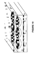
- Figures 3-9 are schematic cross sectional and top views of a semiconductor substrate illustrating one method for forming the structure of the present invention.
- Figure 3 is a cross-sectional view taken along line A-A of Figure 2.
- a semiconductor substrate 301 has a plurality of light sensitive elements 303 (associated with the pixels 203 of Figure 2) formed therein.
- Figure 3 shows the light sensitive element 303 as a photodiode, though other substitutes and equivalents may be used. Details of forming the photodiode and other associated circuitry are known in the prior art and will not be repeated herein to avoid obscuring the present invention. However, examples of the prior art may be seen in U.S. Patent No. 5,904,493 and U.S. Patent No. 6,320,617.
- an optically transparent (in at least a portion of the visible spectrum) base material 305 is formed over the substrate 301.
- the base material 305 may be formed using a blanket deposition process, or alternatively, using a spin on method.
- the base material is an epoxy or an acrylic. These materials are chosen because of their stability, each of handling, or appropriate index of refraction. As will be seen below, it is important that the base material have a relatively low index of refraction. For an epoxy or acrylic material, the index of refraction is in the 1.4 to 1.5 range.
- a suitable material is polymethylmethacrylate (PMMA) or polyglycidylmethacrylate (PGMA).
- the base material may be an oxide.
- the base material may be formed from any optically transparent material having a relatively low index of refraction.
- the base material 305 has the advantage of being substantially planar. It is desirable to have the base material 305 have a top surface that is as planar and smooth as possible. Nevertheless, a blanket deposition, such as by chemical vapor deposition, may also be suitable.
- the thickness of the base material 305 is on the order of 2 to 2.5 microns. However, thinner or thicker layers of the base material 305 may also be used, depending on various design parameters, such as desired focal length of the micro-lens.
- the resin layer 307 is deposited.
- the resin layer 307 is also referred to as a sacrificial layer, and in one embodiment, is a phenyl resin. Because the resin layer 307 will be used as a sacrificial layer, again, there is some flexibility in the precise material used for the resin layer 307.
- the resin layer 307 will need to be patterned. Because of this, it is efficient to use a photoresist type material (such as a phenyl resin) as the resin layer 307. In that way, the resin layer 307 can be "directly patterned" by simply the use of a photolithography apparatus and a developing process.
- a photoresist type material such as a phenyl resin
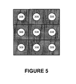
- the resin layer 307 is patterned and developed to remove portions 308 of the resin layer 307.
- the portions 308 of the resin layer 307 that are removed are generally over the light sensitive elements 303 and are circular in shape.
- a top view of the resin layer 307 showing portions removed is shown in Figure 5.
- the removed portions 308 of the resin layer 307 is related to the concave micro-lens to be eventually formed.
- the specific shape and dimensions of the removed portions shown in Figures 4 and 5 is but one specific embodiment of the present invention. Other specific implementations are possible.
- the size of the portions 308 shown in Figures 4 and 5 may be made smaller or larger depending upon the desired size of the micro-lenses to be formed. A larger size for the portion 308 will result in a larger micro-lens, and vice versa.
- an anisotropic dry etch is performed using the reflowed resin layer 307 as an etching mask.
- the etch is a reactive ion etch using O 2 as the primary gas and CH 3 as a secondary gas.
- the etching ratio between the base material 305 and the resin layer 307 is on the order of 1.0 to 1.5.
- the underlying base material 305 is etched faster than the resin layer 307.
- the etching process is complete when the resin layer 307 is removed.
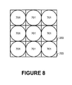
- the spacing between adjacent micro-lenses can be varied by controlling the spacing of the removed portions 308 formed in the resin layer 307. Small removed portions 308 that are spaced far apart from each other will result in relatively small micro-lenses and large gaps between the resultant micro-lenses. Large removed portions 308 will result in large resultant micro-lenses with small gaps. Moreover, by employing over-etching techniques during etching of the base material 305 and the resin layer 307, the gaps between adjacent micro-lenses can be reduced to zero. It can be appreciated that the size of the removed portions 308, the etching length, the composition of the base material 305 and resin layer 307, and other process/design factors can be varied to achieve the desired result for the characteristics of the micro-lenses.
- a fill material 311 is formed over the base material 305 and micro-lens 701.
- the fill material 311 should have a relatively high index refraction that is higher than the base material 305 such that bending and focusing of incident light onto the light sensitive elements 303 takes place.
- the fill material 311 has an index of refraction of between 1.6 and 1.8.
- One example of the fill material 311 is an optically transparent polyimide.
- the thickness of the polyimide layer 311 is on the order of 3 to 4 microns.
- the polyimide layer 311 is typically applied using spin coating.
- a minimal spacing between micro-lenses can be more easily achieved. This improves the fill factor and efficiency in gathering light, thereby improving the sensitivity.
- the concave shape of the micro-lenses provides advantages in available packaging techniques, which in turn can minimize particles and dust from interfering with the image sensor.
- the color filters can be formed using conventional methods either on top of the micro-lenses or in between the micro-lenses and the light sensitive elements 303.
- the use of a concave shaped micro-lens results in a relatively short focal length. This in turn allows for higher integration densities.
Landscapes
- Solid State Image Pick-Up Elements (AREA)
Applications Claiming Priority (2)
| Application Number | Priority Date | Filing Date | Title |
|---|---|---|---|
| US281012 | 1988-12-07 | ||
| US10/281,012 US20040082096A1 (en) | 2002-10-25 | 2002-10-25 | Method for forming an image sensor having concave-shaped micro-lenses |
Publications (2)
| Publication Number | Publication Date |
|---|---|
| EP1414071A2 true EP1414071A2 (fr) | 2004-04-28 |
| EP1414071A3 EP1414071A3 (fr) | 2005-08-24 |
Family
ID=32069400
Family Applications (1)
| Application Number | Title | Priority Date | Filing Date |
|---|---|---|---|
| EP03256674A Withdrawn EP1414071A3 (fr) | 2002-10-25 | 2003-10-23 | Procédé de fabrication d'un capteur d'image avec des microlentilles en forme concave |
Country Status (4)
| Country | Link |
|---|---|
| US (1) | US20040082096A1 (fr) |
| EP (1) | EP1414071A3 (fr) |
| CN (1) | CN100499144C (fr) |
| TW (1) | TW200514267A (fr) |
Cited By (2)
| Publication number | Priority date | Publication date | Assignee | Title |
|---|---|---|---|---|
| WO2006001317A1 (fr) * | 2004-06-23 | 2006-01-05 | Toppan Printing Co., Ltd. | Dispositif d'imagerie a l'etat solide, procede de realisation et substrat pour dispositif d'imagerie a l'etat solide |
| EP1643563A3 (fr) * | 2004-09-30 | 2009-12-23 | STMicroelectronics, Inc. | Structure de micro-lentille pour un dispositif optoélectronique semi-conducteur et procédé de fabrication |
Families Citing this family (5)
| Publication number | Priority date | Publication date | Assignee | Title |
|---|---|---|---|---|
| JP2003112321A (ja) * | 2001-10-02 | 2003-04-15 | Sony Corp | 加工用マスター基材及び同マスター基材の製造方法 |
| JP4207599B2 (ja) * | 2003-02-24 | 2009-01-14 | ソニー株式会社 | 液晶パネルの製造方法 |
| CN100517739C (zh) * | 2004-06-23 | 2009-07-22 | 凸版印刷株式会社 | 固态成像装置及其制造方法 |
| KR100835434B1 (ko) * | 2006-12-28 | 2008-06-04 | 동부일렉트로닉스 주식회사 | 시모스 이미지 센서의 마이크로 렌즈의 제조방법 |
| US10290670B2 (en) * | 2016-06-28 | 2019-05-14 | Omnivision Technologies, Inc. | Resonant-filter image sensor and associated fabrication method |
Family Cites Families (13)
| Publication number | Priority date | Publication date | Assignee | Title |
|---|---|---|---|---|
| US5225935A (en) * | 1989-10-30 | 1993-07-06 | Sharp Kabushiki Kaisha | Optical device having a microlens and a process for making microlenses |
| JP2597037B2 (ja) * | 1990-07-09 | 1997-04-02 | シャープ株式会社 | 固体撮像装置の製造方法 |
| JPH0475384A (ja) * | 1990-07-17 | 1992-03-10 | Sharp Corp | 固体撮像素子 |
| JPH0774331A (ja) * | 1993-09-02 | 1995-03-17 | Nikon Corp | マイクロレンズ付き固体撮像素子及びその製造方法 |
| JPH0927608A (ja) * | 1995-05-11 | 1997-01-28 | Sony Corp | 固体撮像装置とその製造方法 |
| JPH0964325A (ja) * | 1995-08-23 | 1997-03-07 | Sony Corp | 固体撮像素子とその製造方法 |
| JP3571909B2 (ja) * | 1998-03-19 | 2004-09-29 | キヤノン株式会社 | 固体撮像装置及びその製造方法 |
| US6730459B2 (en) * | 2000-07-27 | 2004-05-04 | Seiko Epson Corporation | Microlens array, method for fabricating the same and optical devices |
| JP2002110953A (ja) * | 2000-10-04 | 2002-04-12 | Toshiba Corp | 固体撮像装置 |
| US20020102498A1 (en) * | 2001-01-31 | 2002-08-01 | Chih-Hsing Hsin | Method for forming biconvex microlens of image sensor |
| DE10121530B4 (de) * | 2001-05-03 | 2005-06-09 | Infineon Technologies Ag | Lichtleiteranordnung zur seriellen, bidirektionalen Signalübertragung, optische Leiterplatine und Herstellungsverfahren |
| JP4213897B2 (ja) * | 2001-08-07 | 2009-01-21 | 株式会社日立製作所 | マイクロレンズアレイの転写原型の製造方法 |
| US20030146528A1 (en) * | 2002-02-01 | 2003-08-07 | Kuo-Jui Huang | Method for manufacturing microlens light guide |
-
2002
- 2002-10-25 US US10/281,012 patent/US20040082096A1/en not_active Abandoned
-
2003
- 2003-10-08 TW TW092128003A patent/TW200514267A/zh unknown
- 2003-10-23 EP EP03256674A patent/EP1414071A3/fr not_active Withdrawn
- 2003-10-24 CN CNB2003101043665A patent/CN100499144C/zh not_active Expired - Lifetime
Cited By (4)
| Publication number | Priority date | Publication date | Assignee | Title |
|---|---|---|---|---|
| WO2006001317A1 (fr) * | 2004-06-23 | 2006-01-05 | Toppan Printing Co., Ltd. | Dispositif d'imagerie a l'etat solide, procede de realisation et substrat pour dispositif d'imagerie a l'etat solide |
| US7737044B2 (en) | 2004-06-23 | 2010-06-15 | Toppan Printing Co., Ltd. | Solid state imaging device, manufacturing method of the same, and substrate for solid state imaging device |
| US8004028B2 (en) | 2004-06-23 | 2011-08-23 | Toppan Printing Co., Ltd. | Solid state imaging device, manufacturing method of the same, and substrate for solid state imaging device |
| EP1643563A3 (fr) * | 2004-09-30 | 2009-12-23 | STMicroelectronics, Inc. | Structure de micro-lentille pour un dispositif optoélectronique semi-conducteur et procédé de fabrication |
Also Published As
| Publication number | Publication date |
|---|---|
| CN100499144C (zh) | 2009-06-10 |
| EP1414071A3 (fr) | 2005-08-24 |
| US20040082096A1 (en) | 2004-04-29 |
| CN1505163A (zh) | 2004-06-16 |
| TW200514267A (en) | 2005-04-16 |
Similar Documents
| Publication | Publication Date | Title |
|---|---|---|
| US6737719B1 (en) | Image sensor having combination color filter and concave-shaped micro-lenses | |
| EP1494289B1 (fr) | Capteur d'image comprenant un réseau de microlentilles separé par structures des tranchées et son procédé de fabrication | |
| EP1414072B1 (fr) | Capteur d'image avec de microlentilles plus grands dans des régions périphériques | |
| US6861280B2 (en) | Image sensor having micro-lenses with integrated color filter and method of making | |
| US11404463B2 (en) | Color filter array, imagers and systems having same, and methods of fabrication and use thereof | |
| US10192916B2 (en) | Methods of fabricating solid-state imaging devices having flat microlenses | |
| CN101202248A (zh) | 图像传感器及其制造方法 | |
| EP1414071A2 (fr) | Procédé de fabrication d'un capteur d'image avec des microlentilles en forme concave | |
| EP1414070A2 (fr) | Capteur d'image comprenant des microlentilles de forme concave | |
| CN100405607C (zh) | 具有用脊结构隔开的微透镜的图象传感器及其制造方法 | |
| EP1414076A2 (fr) | Procédé de fabrication des filtres colorés planaires dans un capteur d'image | |
| TWI275188B (en) | Image sensor having reduced stress color filters and method of making | |
| US20090068599A1 (en) | Method of manufacturing image sensor |
Legal Events
| Date | Code | Title | Description |
|---|---|---|---|
| PUAI | Public reference made under article 153(3) epc to a published international application that has entered the european phase |
Free format text: ORIGINAL CODE: 0009012 |
|
| AK | Designated contracting states |
Kind code of ref document: A2 Designated state(s): AT BE BG CH CY CZ DE DK EE ES FI FR GB GR HU IE IT LI LU MC NL PT RO SE SI SK TR |
|
| AX | Request for extension of the european patent |
Extension state: AL LT LV MK |
|
| RAP1 | Party data changed (applicant data changed or rights of an application transferred) |
Owner name: OMNIVISION INTERNATIONAL HOLDING LTD |
|
| PUAL | Search report despatched |
Free format text: ORIGINAL CODE: 0009013 |
|
| AK | Designated contracting states |
Kind code of ref document: A3 Designated state(s): AT BE BG CH CY CZ DE DK EE ES FI FR GB GR HU IE IT LI LU MC NL PT RO SE SI SK TR |
|
| AX | Request for extension of the european patent |
Extension state: AL LT LV MK |
|
| AKX | Designation fees paid |
Designated state(s): AT BE BG CH CY CZ DE DK EE ES FI FR GB GR HU IE IT LI LU MC NL PT RO SE SI SK TR |
|
| STAA | Information on the status of an ep patent application or granted ep patent |
Free format text: STATUS: THE APPLICATION IS DEEMED TO BE WITHDRAWN |
|
| 18D | Application deemed to be withdrawn |
Effective date: 20060225 |