EP1414156A1 - Vorrichtung zum Takten von digitalen und analogen Schaltungen auf einem gemeinsamen Substrat und Verfahren dazu - Google Patents
Vorrichtung zum Takten von digitalen und analogen Schaltungen auf einem gemeinsamen Substrat und Verfahren dazu Download PDFInfo
- Publication number
- EP1414156A1 EP1414156A1 EP20030028094 EP03028094A EP1414156A1 EP 1414156 A1 EP1414156 A1 EP 1414156A1 EP 20030028094 EP20030028094 EP 20030028094 EP 03028094 A EP03028094 A EP 03028094A EP 1414156 A1 EP1414156 A1 EP 1414156A1
- Authority
- EP
- European Patent Office
- Prior art keywords
- digital
- analog
- circuit
- signal
- frequency
- Prior art date
- Legal status (The legal status is an assumption and is not a legal conclusion. Google has not performed a legal analysis and makes no representation as to the accuracy of the status listed.)
- Granted
Links
Images


Classifications
-
- G—PHYSICS
- G06—COMPUTING OR CALCULATING; COUNTING
- G06F—ELECTRIC DIGITAL DATA PROCESSING
- G06F3/00—Input arrangements for transferring data to be processed into a form capable of being handled by the computer; Output arrangements for transferring data from processing unit to output unit, e.g. interface arrangements
- G06F3/05—Digital input using the sampling of an analogue quantity at regular intervals of time, input from a/d converter or output to d/a converter
-
- G—PHYSICS
- G06—COMPUTING OR CALCULATING; COUNTING
- G06F—ELECTRIC DIGITAL DATA PROCESSING
- G06F1/00—Details not covered by groups G06F3/00 - G06F13/00 and G06F21/00
- G06F1/04—Generating or distributing clock signals or signals derived directly therefrom
- G06F1/08—Clock generators with changeable or programmable clock frequency
Definitions
- This invention relates to a monolithic semiconductor substrate embodying both digital and analog circuits and, more particularly, to an apparatus and method for reducing noise transferred from digital circuits to analog circuits without limiting digital circuit performance,
- Audio acquisition includes any device which receives and records an audio waveform, and which samples and quantizes that waveform according to discrete time intervals.
- Audio transmission may include digital audio reproduction -i.e., demodulation and digital processing circuits necessary to manipulate digital information.
- Audio acquisition can be accomplished using various types of modulation schemes, such as pulse code modulation, delta-sigma modulation, etc. Regardless of the modulation scheme used, proper audio recording requires the incoming analog signal be sampled at a frequency of at least twice the incoming audio frequency to achieve error-free sampling. Sampling less than the aforesaid minimum causes aliasing problems. During each sample interim, quantization is used to preserve corresponding amplitude information. While sampling records time slices, quantization records amplitude information within each time slice. The combination of sampling and quantization for a given modulation technique thereby completely preserves the audio signal in digital form. Accordingly, audio acquisition must employ analog circuitry useful in sampling (e.g., sample-and-hold circuits) and quantization (e.g., clocked comparator circuits).
- analog circuitry useful in sampling e.g., sample-and-hold circuits
- quantization e.g., clocked comparator circuits
- audio reproduction includes, for example, demodulation circuits, reproduction processing circuits, demultiplexers, digital-to-analog converters, output sample-and-hold circuits, etc. Accordingly, digital audio reproduction is necessary to present back, possibly in digitally processed form, the analog signal previously recorded through analog acquisition.
- DSP digital signal processor
- a DSP is used to manipulate digitally acquired binary numbers.
- the ease by which digital numbers can be manipulated by a DSP adds importance to reasons why it may be desirable to convert an analog audio signal to a digital audio signal, and why the manipulated data can thereafter be converted back to analog form.
- the DSP can easily perform rapid manipulation of that data. DSP operations are prevalent in the telecommunication industry, and are usually found in modems, vocoders and transmultiplexers, etc.
- Examples of circuits used to convert an analog audio signal to a digital signal is an analog/digital ("A/D") converter.
- a digital-to-analog circuit is often referred to as a (“D/A”) converter.
- Placing the DSP between the AID and D/A converter allows manipulation of the digital information preferably in real time.
- a clock manager may be used to clock the multiple digital and analog subsystems embodied upon the substrate.
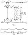
- Fig. 1 illustrates an example of an input stage of a typical modulator used, e.g., in a delta sigma A/D converter.
- Switches Q1 and Q2 are activated and deactivated in rapid succession to sample differential analog input signals +VIN and -VIN.
- the analog signals may be periodically sampled according to the timing diagram shown in Fig. 2.
- Switches Q 1 are closed during times when "signal 1" (shown in Fig. 2) transitions to a logic high value.
- switches Q2 are closed during times when signal 2 of Fig. 2 transitions to a logic high value.
- a delta sigma A/D converter generally comprises a modulator and a digital decimation filter.
- the modulator samples the analog input at a high frequency and low resolution.
- the resulting quantization noise from the sampling event is shaped by the modulator so that its noise density is lowest over the frequency band of interest.
- typically the low frequencies are of interest so that quantization noise is shaped to be the lowest at low frequencies and greatest at high frequencies.
- the digital decimation filter takes the noise shaped modulator output, low pass filters that output, and decimates it to the audio sample rate.
- the resolution of the decimation filter output is much greater than the modulator output, since the bandwidth is reduced and because the high frequency modulator noise has been low pass filtered.
- the A/D converter therefore requests sampling of the analog input. Similar to an A/D converter, sampling is required in a D/A converter which employs an interpolation filter.
- An interpolation filter generally increases the sample rate, and the delta sigma (or sigma delta) modulator creates a one bit output stream which shapes the quantization noise output.
- the D/A switched capacitor converts the one bit output to a positive or negative reference (VREF) value, and low pass filters smoothes the discrete voltage steps from the switched capacitor circuit. Interpolation is generally performed in the DSP portion of the substrate, whereas the D/A switched capacitor and continuous time filters are in analog portions of the substrate.
- VREF positive or negative reference
- the audio sampling rate (fs) is typically 44.1 kHz or 48kHz.
- the analog modulator sampling rate (Fovr) is many times the audio sample rate. Typically, Fovr is 128fs or 256fs. For every one audio sample, the modulator samples 128 or 256 times.
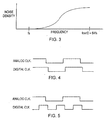
- a plot of a typical delta sigma modulator operating at 128fs is shown in Fig. 3.
- This one bit output represents a signal which switches between a positive reference voltage (i.e., "1 ”) and a negative reference voltage (i.e., "0"), If the input to the modulator is at a DC level, then the average of these one bit samples is equal to the DC level applied to the input. For instance, if the input voltage is zero, the output bit stream will consist of an equal number of 1 s and 0s. This could be a square wave with a frequency of Fovr/2. In this case, all the quantization noise is localized to a tone at Fovr/2.
- the output of a modulator will not be an exact square wave for a DC level of zero on the input, however, it will have a significant amount of noise energy in a tone at or near Fovr/2.
- the frequency of this tone will vary slightly and multiple tones may appear at and around Fovr/2. Care must be taken to prevent these tones from mixing with any digital noise at Fovr/2 and shifting down to the baseband.
- Digital noise on a mixed signal IC can couple into the analog circuitry in a variety of ways.
- a common means is through the substrate.
- Transistors or interconnect on an integrated circuit have some form of capacitive coupling to and from the monolithic substrate.
- Large amounts of digital circuits switching at high frequencies can capacitively couple a significant amount of energy into the substrate causing currents to flow and the voltage to vary. Since the substrate is common between the analog and the digital portions, this energy will couple into the analog circuitry and the analog signal path.
- Noise from the substrate can couple into the analog signal path in a linear or non-linear fashion. If it couples linearly (i.e.. the amount of coupling is independent of the analog signal level) then the coupling signal is seen directly in the analog signal. If it couples non-linearly (i.e., the amount of coupling is dependent on the analog signal level) the coupling signal will then mix with the analog signal. The sum and difference frequencies of the original analog signal and the coupling signal are seen on the resulting analog signal.
- Linear coupling could occur between the substrate and the bottom plate of a poly-poly capacitor, while non-linear coupling could occur between the substrate and the source/drain of a transistor.
- the capacitance between the substrate and the bottom plate of a poly-poly capacitor does not vary significantly with the voltage difference.
- the capacitance between the substrate and the source or drain of a transistor does vary with the voltage difference. This non-linearity causes the signal to modulate the other signal, the result of which is a sum and difference frequency in the output signal.
- delta sigma modulators produces tones near Fovr/2. If there is signal energy in the substrate from the digital circuit position with a frequency of Fovr/2, this will mix with the tones and produce difference frequencies in the baseband (0 to fs/2). In order to prevent this from happening, it is important to ensure that very little digital circuitry operates at Fovr/2.
- DSPs Software running in DSPs can produce digital noise in the substrate. Different instructions use different physical circuitry. For instance, a multiply instruction uses the multiply unit, while a move instruction does not. An operation that operates on the contents of register and stores the result back in a register does not use data memory, while memory-to-memory operations do. Typically, memory-to-memory operations and multiply instructions consume the most power, while move instructions and register-to-register operations consume less. The more power consumed, typically, the more noise is coupled into the substrate. Software programs on DSPs typically repeat at powers of two times the sample rate. This repeating produces digital noise in the substrate at that rate.
- Convertersor modulators which operate at powers of two times the sampling rate (i.e., 2Nfs) receive noise, via the monolithic substrate, from processors or DSPs operating at 2Nfs, where N is an integer value of 1, 2, 3, 4, etc.
- Noise imputed across the substrate from the digital circuits to the analog modulator typically affect the switched capacitors of the modulator. It is commonly known that when switched capacitor circuits are integrated on the same IC with a significant amount of digital circuitry, the switches need to be turned off at a time when the digital circuitry is quiet. Traditionally, this has been done by clocking the digital and analog circuitry at the same frequency, but with the digital clock delayed relative to the analog clock. The digital switching occurs shortly after the switches are closed and the digital noise from the switching settles prior to the next sample event as shown in Fig. 4.
- Switch capacitor circuits require two non-overlapping clocks derived from the analog clock of Fig. 4 to control the switches. Exemplary switches within a switched capacitor network of a conventional modulator are shown in Fig. 1, and non-overlapping clocks are shown in Fig. 2.
- the digital clock frequency is higher than the analog clock frequency, however, the digital clock is still delayed relative to the analog clock.
- This implementation allows the digital circuitry to be clocked faster, which can be advantageous, at the cost of reduced quiet time.
- Fig. 5 illustrates a digital clock transitioning at twice the speed of the analog clock.
- the digital circuitry can typically operate at a much higher frequency than the analog circuitry.
- the DSP can run at clock frequencies of 100 MHz and above.
- the switch capacitor circuits are typically clocked at a few MHz.
- To achieve maximum performance from the DSP it is best to operate it with the fastest clock possible.
- the quiet time immediately preceding each analog transition i.e., sample
- the quiet time immediately preceding each analog transition decreases to the point of significantly degrading performance of the analog modulator by providing more noise to switched capacitors.
- the problems outlined above are in large part solved by an improved clocking scheme.
- the clocking scheme hereof minimizes the effects of digitally created noise upon analog circuits, wherein the digital and analog circuits share a common monolithic semiconductor substrate.
- the monolithic substrate is a semiconductor chip, comprised essentially of silicon or gallium arsenide. Clocking of the digital circuits are controlled relative to the times in which analog circuits perform sampling on an incoming audio (analog) input signal. By deleting or suppressing digital pulses during a latter portion of each sample interval, noise transferal during digital clock transitions do not interfere with the integrity of the sampled analog input signal. Since there are no transitions during the latter portion of each sample interval, there can be no digitally created noise arising at this critical sampling time.
- the converters are advantageously operated with an oversampling rate (Fovr) that is not a power of two of the sample rate (fs). For instance, if the oversampling rate is 96fs, Fovr/2 is 48fs, which is not a power of two. More specifically, 96 or 48 is not a number which can be derived by 2N, where N is a positive, integer number. Since it is uncommon to operate the digital circuitry at a non-power of two rate, there should be little noise power in the substrate at Fovr/2. This means the tones that exist near Fovr/2 in the delta sigma modulated signals will not be mixed into the baseband.
- Fovr oversampling rate
- the difference frequency between a non-power-of-two frequency (i.e., 48fs) and a power-of-two frequency (i.e., 32fs and 64fs), which are the closest power of two rates, is 16fs.
- the 16fs energy will be generated in the analog signals, however, it is far from the baseband and will be filtered by the decimation filter in the AID converter or the switched capacitor and continuous time filters in a D/A.
- the digital circuit is advantageously clocked at full speed, whereby one or more pulses from the clock prior to the sensitive analog sample times is/are removed.
- This enables the DSP to operate at full speed most of the time and for the substrate to be quiet the minimum amount needed by the analog circuitry.
- a substantial percentage of the original digital clocking frequency is maintained. It is determined that a critical sampling time occurs primarily during the latter portions of each sample interval. The early portions do not significantly affect the final sampled value provided, however, the semiconductor substrate is quiet during the latter portions. Eliminating digital pulses only during the latter portions thereby minimizes the reduction in digital clocking frequency.
- a PLL and clock dividers can be used to create the various clock rates which are required by a typical mixed signal integrated circuit.
- the integrated circuit requires one timing source.
- This timing source can be an on chip oscillator or an external clock input. It can also be derived from a serial bitstream input to the chip.
- the on-chip or external clock can be divided by M prior to being applied to the phase-locked loop ("PLL") and the feedback divider in the PLL can multiply the input to the PLL by N.
- the output of the PLL can further be divided, if needed, by another factor P to create the oversampling clock (Fovr).
- the frequency divisor P can be a part of a clock manager (shown in Fig. 7). If a serial bitstream with clock information encoded into it is applied to the PLL, no division by M is possible unless a second PLL is used.
- the input signal Sin applied to the PLL from either an external or internal source is clocked at a frequency of Fin.
- Din is the frequency of the clock encoded in a data timing source
- Fvco is the frequency of the PLL output
- Fovr is the frequency of the converter oversampling clock.
- the various signals and associated frequencies are shown in Fig. 6.
- Fig. 6 also depicts a divider 10, a multiplexer 12, a phase detector (“PD") 14, a loop filter 16, a voltage controlled oscillator (“VCO”) 18 and a feedback divider 19, the latter elements of which are in a PLL.
- Another divider 17 (with division factor P) may output a signal from the PLL clocked at an oversampled frequency Fovr.
- the oversampling clock (Fovr) will not be a power of two and will prevent digital noise at power of two frequencies in the substrate from mixing the Fovr/2 tones in the sigma delta modulated signal into the baseband.
- the oversampling clock (Fovr) will not be a power of two and will prevent digital noise at power of two frequencies in the substrate from mixing the Fovr/2 tones in the sigma delta modulated signal into the baseband.
- one mode of the present implementation accepts a 64fs input clock (Fin) multiplied by 24 (N) to create a 1536fs VCO clock (Fvco), and divides the VCO clock by 16 to create 96fs oversampling clock (Fovr).
- Fvco is determined as a non power-of-two factor of fs, or as a power-of-two factor divided by a prime number of at least three.
- Frequency multiplier 20 is used to frequency multiply a clocking signal derived either external or internal to the integrated circuit.
- the frequency multiplied sampling frequency is a multiple of the incoming frequency Fin, and is shown as Fvco.
- a frequency multiplier can be employed using various types of amplifiers and/or phase-locked loops. For example, frequency multiplication can be carried out using a non-linear amplifier which generates harmonics in its output current and a tuned load that resonates at one of the harmonics.
- frequency multiplication can be carried out using non-linear capacitance of a junction (semiconductor) diode to couple energy from the input circuit, which is tuned to the fundamental frequency of the output circuit, which is tuned to the desired harmonic.
- a junction semiconductor
- non-linear capacitance coupling represent two frequency multiplication examples, a third being a phase-locked loop with a frequency divider in the feedback loop.
- frequency multiplier 20 includes a phase-locked loop (PLL).
- PLL comprises any electronic circuit which locks an oscillator in phase with an input signal.
- the PLL tracks a carrier or synchronizing signal whose sampling frequency fs varies somewhat with time.
- the basic frequency multiplier circuit 20, employed as a PLL includes a frequency divider 19, a phase detector (PD) circuit 22, a voltage controlled oscillator (VCO) circuit 24, and another frequency divider circuit 26.
- Phase detector 22 detects and tracks small differences in phase and frequency between the incoming baseband signal Sin and the frequency divided signal at the output of frequency divider circuit 26. Output pulses from detector 22 are proportional to the phase differences of those incoming signals.
- a low-pass filter comprising, e.g., resistor 28 and capacitor 30, removes alternating current (AC) components.
- the low-pass filter output is directed, as a direct current (DC) signal, into oscillator 24.
- Input voltage to oscillator 24 acts to change the output frequency of oscillator 24 to that of the carrier signal.
- the PLL shown in Fig. 7 is configured as a frequency multiplier by operating oscillator 24 at N/M times the input frequency of the incoming clocking signal transitioning at frequency Fin. Accordingly, the output from oscillator 24 operates at a higher frequency than the incoming clocking signal Sin. In the general loop, the output is driven in a direction that will minimize the error signal - i.e., the phase difference between the output of frequency divider 26 and the sampling signal. Thus, the PLL tends to drive the error signal back toward zero phase difference. Once the two phases are made equal, the oscillator 24 will be locked to a multiple frequency of Fin, and any phase difference between the two signals will be controlled.
- Frequency divider circuit 26 includes any electronic circuit which produces an output signal at a frequency which is an integral submultiple of the frequency of its input signal.
- a frequency division can be conveniently accomplished in two ways: digital division or division by subharmonic triggering. Using the former as an example, many circuits are available to count pulses and thereby provide digital division.
- a bistable circuit or flip-flop produces one output pulse for every two input pulses. By cascading successive flipflops, any desired degree of division can be obtained. Division by power to two can be achieved simply by monitoring the output of the proper stage of the cascade. However, division by other numbers beyond the power of two is required and can be achieved by gating to obtain the proper set of flip-flop conditions.
- Frequency divider circuit 26 thereby employs any number of stages and gate logic necessary to produce an N frequency division. For example, a four stage counter is necessary to produce a frequency divider N of 16, i.e., 24 state.
- Clock manager 25 receives the frequency multiplied DCLK value and produces a corresponding ACLK1, ACLK2 and DSPCLK values.
- Fin after M division can be equal to a Nyquist sampling rate, fs, of 48KHz, and multiplier factor N can be 1536, making Fvco equal to 1536fs, or approximately 67MHz.
- the DSPCLK has one or more 1536fs clock pulses removed prior to the falling edges of ACLK1 and ACLK2. This means that the digital noise from the DSP has settled prior to the analog sampling event.
- the PLL locks to the baseband sample rate fs or some multiple of fs (e.g., 1536fs), from which the analog (ACLK1 and ACLK2) clocks and DSP (DSPCLK) clocks are generated via clock manager 25.
- N The N division factor of divider 26, or the combination of factors M and N, produce a factor determined by a power-of-two times a prime number equal to or greater than three.
- F vco e.g., 1536fs
- the progression of B to C to D is that of prime number beginning with three and increasing to 5, 7, etc.
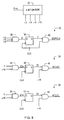
- Clock manager 25 comprises a clock divider and some logic to generate the desired clocks. Referring to Fig. 8, various portions of the clock manager are shown. In particular, a 4-bit divider (or counter) 30 is shown which receives the multiplied baseband signal Sin. The frequency of Fvco is divided by factors of 2, 4, 8 and 16 to produce corresponding signals used by logic circuits 32. 34 and 36 to produce respective clocks for the DSP, and the modulator (i.e., switched capacitor circuit) both of which are embodied on a single substrate.
- Circuit 32 includes a three input AND gate 38, the output of which is fed into a delay input of a D-type flip flop 40.
- the non-inverted output of flip flop 40 is then presented as a "Y" signal, which is then inverted and applied to one input of AND gate 42.
- the output of AND gate 42 is DSPCLK.
- Circuit 34 includes a two input AND gate 44, the output of which is fed into a delay input of a D-type flip flop 46. The non-inverted output of flip flop 46 is then presented to AND gate 48. The output of AND gate 48 is ACLK2.
- ACLK1 is produced similar to ACLK2, except ACLK1 is produced using AND gate 50, D-type flip flop 52 and AND gate 54 connected as shown in circuit 36.
- Frequency divider circuit 30 divides by integer to the power of two.
- Logic 32, 34 and 36 includes any and all functionality necessary to delete at least one clock cycle of DSPCLK at regular count intervals.
- Signal X shown in circuit 32 occurs once every eight cycles of CLK, and signal Y is delayed one cycle of CLK.
- Signal Y thereafter defines respective clock pulses Z1 and Z2 once every eight cycles of CLK.
- Each clock pulse Z2 occurs between respective pairs of pulses Z1.
- the DSPCLK is created by ANDing the Fvco with signal Y.
- Signal Y is the same as signal X except delayed by one half of the VCO clock period.
- Signal X is generated by ANDing Fvco/2, the inverted version of Fvco/4, and the inverted version of fvco/8.
- Signal X goes high at the rising edge of Fvco just prior to the rising edge of the pulse to be removed from Fvco to generate DSPCLK. Since Fvco/2, Fvco/4, and Fvco/8 may transition at slightly different times, X may momentarily glitch just after rising edges of Fvco.
- Signal Y is created to eliminate these glitches prior to gating with Fvco to generate DSPCLK.
- a timing diagram of Fvco, Fvco/2, Fvco/4, Fvco/8, Fvco/16, X, Y, Z1, Z2, ACLK1, ACLK2 and DSPCLK are shown in Fig. 9.
- the non-overlapping clocks ACLK1 and ACLK2 are created by ANDing Fovr and the inverted version of Fovr respectively with the inverted version of signals Z1 and Z2 respectively.
- the signals Z1 and Z2 are created in order to remove the last half Fvco clock cycle from the high time of Fovr and the inverted version of Fovr to create ACLK1 and ACLK2 respectively.
- the signal Z1 is high one half Fvco clock cycle before Fovr goes low and one half Fvco clock cycle after Fovr goes low.
- the signal Z2 is high one half Fvco clock cycle before Fovr goes high and one half Fvco clock cycle after Fovr goes low.
- the signal Z2 is high one half Fvco clock cycle before Fovr goes high and one half Fvco clock cycle after Fovr goes high.
- Z1 and Z2 are created by delaying the signals Z1 a and Z2a by one half of an Fvco clock period.
- Z1 a and Z2a are created by ANDing Y with Fovr and the inverted version of Fovr respectively.
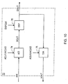
- integrated circuit 70 which illustrates both analog and digital circuits on the same monolithic substrate.
- Integrated circuit 70 includes analog circuitry which acquires an analog (audio) input signal AIN.
- Integrated circuit 70 further includes a digitally operated processor which manipulates digital representations of AIN and reproduces an analog output AOUT from those digital representations.
- integrated circuit 70 includes a mechanism for sampling and quantizing AIN according to discrete time intervals. The sampled AIN signal is then converted to digital format, whereby resulting digital signals are processed using various DSP algorithms. Thereafter, the processed digital signals can be reproduced back as audio signals AOUT. In the interim, the processed digital signals can, if desired, be output as DOUT'.
- Integrated circuit 70 includes any circuit having both analog (sample/quantizer) functions and digital (digital processing and reproduction) functions employed upon a single monolithic substrate.
- Integrated circuit 70 includes an analog-to-digital (A/D) circuit 74 which receives AIN.
- A/D circuit 74 samples AIN, and quantizes the magnitude of the sampled signal during each sample interval.
- A/D circuit 74 may include an analog low pass filter, possibly employed as an integrator, subsequent to the sampling function.
- the output from A/D circuit 74 is represented as a bit stream of digital signals, shown as DOUT.
- AID circuit 74 samples and quantizes according to an analog clocking signal ACLK. If ACLK frequency is large, oversampling attributed to well known deltasigma modulation may occur.
- Delta-sigma modulation produces a DOUT signal having a bit stream of logic 1 s relative to logic Os which is indicative of AIN voltage magnitude.
- A/D circuit 74 encompasses a generalized modulator, and not simply an oversampled modulator.
- A/D circuit 74 includes any circuit which samples and quantizes at a rate defined by an analog clocking signals ACLK1 and ACLK2.
- D/A circuit 76 is clocked by ACLK1/ACKL2
- DSP 78 may be clocked by a digital clocking signal DSPCLK.
- the digital clocking signal can take on several different frequencies depending upon which frequency is selected.
- the digital clocking signal frequency chosen is, however, of higher frequency than the analog clocking signal ACLK1/ACKL2 for the reasons and having the advantages stated above.
- the D/A circuit 76 can be an oversampling type converter, in which an analog portion of the D/A circuit basically functions as reference voltage selector followed by low pass filtering. Either a positive or a negative reference voltage (either +VREF or -VREF) is selected by D/A circuit 76 in accordance with its receipt of a high logic level or a low logic level, respectively.
- DSP 78 includes any unit which processes digital signals with multiply, add and/or delay operations. Those basic operations allow DSP 78 to perform complex digital filtering, digital scaling, decimation and/or interpolation.
- DSP 78 includes input and output devices, an arithmetic logic unit, a control unit, memory, and interconnect buses extending therebetween. Resulting from digital manipulation, DOUT is converted to a processed bit stream denoted as DOUT'.
- Integrated circuit 70 shown in Fig. 10, thereby includes A/D digital recording devices, D/A digital reproduction devices, and DSP digital processing devices, all upon a single monolithic substrate.
- the digital clocking signal is not only user programmable to one of many fixed frequencies, but the frequency chosen is maintained at a higher frequency magnitude than the analog clocking signal.
Landscapes
- Engineering & Computer Science (AREA)
- Theoretical Computer Science (AREA)
- Physics & Mathematics (AREA)
- General Engineering & Computer Science (AREA)
- General Physics & Mathematics (AREA)
- Human Computer Interaction (AREA)
- Compression, Expansion, Code Conversion, And Decoders (AREA)
- Analogue/Digital Conversion (AREA)
- Electric Clocks (AREA)
- Manipulation Of Pulses (AREA)
Applications Claiming Priority (3)
| Application Number | Priority Date | Filing Date | Title |
|---|---|---|---|
| US09/025,157 US6057791A (en) | 1998-02-18 | 1998-02-18 | Apparatus and method for clocking digital and analog circuits on a common substrate to enhance digital operation and reduce analog sampling error |
| EP99907000A EP1057261B1 (de) | 1998-02-18 | 1999-02-12 | Einrichtung und verfahren zum takten von digitalen und analogen schaltungen auf einem gemeinsam substrat zur geräuschverminderung |
| US25157 | 2001-12-19 |
Related Parent Applications (2)
| Application Number | Title | Priority Date | Filing Date |
|---|---|---|---|
| EP99907000A Division EP1057261B1 (de) | 1998-02-18 | 1999-02-12 | Einrichtung und verfahren zum takten von digitalen und analogen schaltungen auf einem gemeinsam substrat zur geräuschverminderung |
| EP99907000.6 Division | 1999-02-12 |
Publications (2)
| Publication Number | Publication Date |
|---|---|
| EP1414156A1 true EP1414156A1 (de) | 2004-04-28 |
| EP1414156B1 EP1414156B1 (de) | 2006-08-30 |
Family
ID=21824368
Family Applications (2)
| Application Number | Title | Priority Date | Filing Date |
|---|---|---|---|
| EP99907000A Expired - Lifetime EP1057261B1 (de) | 1998-02-18 | 1999-02-12 | Einrichtung und verfahren zum takten von digitalen und analogen schaltungen auf einem gemeinsam substrat zur geräuschverminderung |
| EP03028094A Expired - Lifetime EP1414156B1 (de) | 1998-02-18 | 1999-02-12 | Vorrichtung zum Takten von digitalen und analogen Schaltungen auf einem gemeinsamen Substrat und Verfahren dazu |
Family Applications Before (1)
| Application Number | Title | Priority Date | Filing Date |
|---|---|---|---|
| EP99907000A Expired - Lifetime EP1057261B1 (de) | 1998-02-18 | 1999-02-12 | Einrichtung und verfahren zum takten von digitalen und analogen schaltungen auf einem gemeinsam substrat zur geräuschverminderung |
Country Status (7)
| Country | Link |
|---|---|
| US (1) | US6057791A (de) |
| EP (2) | EP1057261B1 (de) |
| JP (1) | JP4091254B2 (de) |
| AT (2) | ATE265060T1 (de) |
| AU (1) | AU2677699A (de) |
| DE (2) | DE69933063T2 (de) |
| WO (1) | WO1999043087A2 (de) |
Families Citing this family (37)
| Publication number | Priority date | Publication date | Assignee | Title |
|---|---|---|---|---|
| US6678243B2 (en) * | 1997-11-14 | 2004-01-13 | Ess Technology, Inc. | Variable codec frame length |
| JP3942790B2 (ja) * | 2000-02-24 | 2007-07-11 | アンリツ株式会社 | 信号分析装置 |
| US6683905B1 (en) * | 2000-04-17 | 2004-01-27 | Rf Micro Devices, Inc. | Dual-mode receiver |
| US6313770B1 (en) * | 2000-06-15 | 2001-11-06 | Sigmatel, Inc | System for sampling an analog signal and method thereof |
| EP1209809A1 (de) * | 2000-11-24 | 2002-05-29 | STMicroelectronics S.r.l. | Vorrichtung und Verfahren zur Erzeugung synchroner numerischer Signale |
| US6492926B2 (en) | 2000-11-24 | 2002-12-10 | Stmicroelectronics S.R.L. | Noise compensation device and method in a discrete time control system |
| US7346048B1 (en) * | 2001-07-31 | 2008-03-18 | Lsi Logic Corporation | Efficient high density voice processor |
| US6693477B2 (en) | 2001-10-22 | 2004-02-17 | Research In Motion Limited | Clock circuit for a microprocessor |
| US6700520B1 (en) * | 2002-09-16 | 2004-03-02 | Motorola, Inc. | Multi-bit continuous time sigma-delta ADC |
| DE10306313B4 (de) * | 2003-02-14 | 2004-12-16 | Infineon Technologies Ag | Verfahren und Vorrichtung zur Erzeugung eines Systemtakts |
| US7937557B2 (en) * | 2004-03-16 | 2011-05-03 | Vns Portfolio Llc | System and method for intercommunication between computers in an array |
| US8068176B2 (en) * | 2004-07-02 | 2011-11-29 | Trident Microsystems (Far East) Ltd. | Noise elimination device for the detection of the vertical sync pulse in video signals |
| US20060038596A1 (en) * | 2004-08-18 | 2006-02-23 | Binan Wang | Delay locked loop circuitry and method for optimizing delay timing in mixed signal systems |
| US7193544B1 (en) * | 2004-09-08 | 2007-03-20 | Northrop Grumman Corporation | Parallel, adaptive delta sigma ADC |
| TWI303929B (en) * | 2005-04-20 | 2008-12-01 | Realtek Semiconductor Corp | Application circuit and method for shaping noise |
| US7904695B2 (en) * | 2006-02-16 | 2011-03-08 | Vns Portfolio Llc | Asynchronous power saving computer |
| US7966481B2 (en) | 2006-02-16 | 2011-06-21 | Vns Portfolio Llc | Computer system and method for executing port communications without interrupting the receiving computer |
| US7904615B2 (en) * | 2006-02-16 | 2011-03-08 | Vns Portfolio Llc | Asynchronous computer communication |
| US7573409B2 (en) * | 2007-03-22 | 2009-08-11 | Vns Portfolio Llc | Variable sized aperture window of an analog-to-digital converter |
| KR101224102B1 (ko) * | 2009-11-05 | 2013-01-21 | 한국전자통신연구원 | 파이프라인 아날로그-디지털 변환기 |
| US9002488B2 (en) * | 2010-02-22 | 2015-04-07 | Cypress Semiconductor Corporation | Clock synthesis systems, circuits and methods |
| US9124413B2 (en) * | 2011-10-26 | 2015-09-01 | Qualcomm Incorporated | Clock and data recovery for NFC transceivers |
| US20180317019A1 (en) | 2013-05-23 | 2018-11-01 | Knowles Electronics, Llc | Acoustic activity detecting microphone |
| US9711166B2 (en) * | 2013-05-23 | 2017-07-18 | Knowles Electronics, Llc | Decimation synchronization in a microphone |
| WO2014189931A1 (en) | 2013-05-23 | 2014-11-27 | Knowles Electronics, Llc | Vad detection microphone and method of operating the same |
| US10020008B2 (en) | 2013-05-23 | 2018-07-10 | Knowles Electronics, Llc | Microphone and corresponding digital interface |
| US10028054B2 (en) | 2013-10-21 | 2018-07-17 | Knowles Electronics, Llc | Apparatus and method for frequency detection |
| US9502028B2 (en) | 2013-10-18 | 2016-11-22 | Knowles Electronics, Llc | Acoustic activity detection apparatus and method |
| US9147397B2 (en) | 2013-10-29 | 2015-09-29 | Knowles Electronics, Llc | VAD detection apparatus and method of operating the same |
| US10045140B2 (en) | 2015-01-07 | 2018-08-07 | Knowles Electronics, Llc | Utilizing digital microphones for low power keyword detection and noise suppression |
| TW201640322A (zh) | 2015-01-21 | 2016-11-16 | 諾爾斯電子公司 | 用於聲音設備之低功率語音觸發及方法 |
| US10121472B2 (en) | 2015-02-13 | 2018-11-06 | Knowles Electronics, Llc | Audio buffer catch-up apparatus and method with two microphones |
| US9478234B1 (en) | 2015-07-13 | 2016-10-25 | Knowles Electronics, Llc | Microphone apparatus and method with catch-up buffer |
| JP6789727B2 (ja) * | 2016-08-31 | 2020-11-25 | 新日本無線株式会社 | アナログデジタル混在回路 |
| JP6834299B2 (ja) * | 2016-09-27 | 2021-02-24 | セイコーエプソン株式会社 | 回路装置、物理量測定装置、電子機器及び移動体 |
| US10965309B1 (en) * | 2020-01-16 | 2021-03-30 | Raytheon Company | Digital delta-sigma modulator with dynamically adjustable output frequency band |
| CN114389607B (zh) * | 2021-12-24 | 2024-06-04 | 莱弗利科技(苏州)有限公司 | 一种低噪声干扰的数模混合芯片 |
Citations (6)
| Publication number | Priority date | Publication date | Assignee | Title |
|---|---|---|---|---|
| US4403350A (en) * | 1980-04-24 | 1983-09-06 | Nissan Motor Company Limited | Interference avoidance electronic system for an automotive vehicle |
| EP0413287A2 (de) * | 1989-08-18 | 1991-02-20 | Fujitsu Limited | Ein-Chip-Halbleitervorrichtung, die eine Verarbeitungsschaltung für digitales Signal und eine Verarbeitungsschaltung für analoges Signal enthält |
| US5055800A (en) * | 1990-04-30 | 1991-10-08 | Motorola, Inc. | Fractional n/m synthesis |
| EP0487743A1 (de) * | 1990-06-11 | 1992-06-03 | Oki Electric Industry Company, Limited | Mikrorechner mit eingebautem umsetzer |
| US5422807A (en) * | 1992-08-31 | 1995-06-06 | Microchip Technology Incorporated | Microcontroller with improved A/D conversion |
| EP0803791A1 (de) * | 1989-07-07 | 1997-10-29 | STMicroelectronics Limited | Takterzeugungsschaltung |
Family Cites Families (4)
| Publication number | Priority date | Publication date | Assignee | Title |
|---|---|---|---|---|
| JP2534711B2 (ja) * | 1987-06-29 | 1996-09-18 | 日本電気株式会社 | オ−バ−サンプル型a・d変換器 |
| US4950999A (en) * | 1989-03-06 | 1990-08-21 | Agnello Anthony M | Self-contained, real-time spectrum analyzer |
| DE4214611A1 (de) * | 1992-05-02 | 1993-11-04 | Philips Patentverwaltung | Schaltungsanordnung zum verarbeiten digitaler signale |
| US5543792A (en) * | 1994-10-04 | 1996-08-06 | International Business Machines Corporation | Method and apparatus to enhance the efficiency of storing digitized analog signals |
-
1998
- 1998-02-18 US US09/025,157 patent/US6057791A/en not_active Expired - Lifetime
-
1999
- 1999-02-12 JP JP2000532917A patent/JP4091254B2/ja not_active Expired - Lifetime
- 1999-02-12 AT AT99907000T patent/ATE265060T1/de not_active IP Right Cessation
- 1999-02-12 EP EP99907000A patent/EP1057261B1/de not_active Expired - Lifetime
- 1999-02-12 AT AT03028094T patent/ATE338379T1/de not_active IP Right Cessation
- 1999-02-12 WO PCT/US1999/003137 patent/WO1999043087A2/en not_active Ceased
- 1999-02-12 DE DE69933063T patent/DE69933063T2/de not_active Expired - Lifetime
- 1999-02-12 DE DE69916585T patent/DE69916585T2/de not_active Expired - Lifetime
- 1999-02-12 AU AU26776/99A patent/AU2677699A/en not_active Abandoned
- 1999-02-12 EP EP03028094A patent/EP1414156B1/de not_active Expired - Lifetime
Patent Citations (6)
| Publication number | Priority date | Publication date | Assignee | Title |
|---|---|---|---|---|
| US4403350A (en) * | 1980-04-24 | 1983-09-06 | Nissan Motor Company Limited | Interference avoidance electronic system for an automotive vehicle |
| EP0803791A1 (de) * | 1989-07-07 | 1997-10-29 | STMicroelectronics Limited | Takterzeugungsschaltung |
| EP0413287A2 (de) * | 1989-08-18 | 1991-02-20 | Fujitsu Limited | Ein-Chip-Halbleitervorrichtung, die eine Verarbeitungsschaltung für digitales Signal und eine Verarbeitungsschaltung für analoges Signal enthält |
| US5055800A (en) * | 1990-04-30 | 1991-10-08 | Motorola, Inc. | Fractional n/m synthesis |
| EP0487743A1 (de) * | 1990-06-11 | 1992-06-03 | Oki Electric Industry Company, Limited | Mikrorechner mit eingebautem umsetzer |
| US5422807A (en) * | 1992-08-31 | 1995-06-06 | Microchip Technology Incorporated | Microcontroller with improved A/D conversion |
Also Published As
| Publication number | Publication date |
|---|---|
| WO1999043087A2 (en) | 1999-08-26 |
| DE69916585T2 (de) | 2004-08-12 |
| AU2677699A (en) | 1999-09-06 |
| ATE265060T1 (de) | 2004-05-15 |
| DE69916585D1 (de) | 2004-05-27 |
| US6057791A (en) | 2000-05-02 |
| JP4091254B2 (ja) | 2008-05-28 |
| WO1999043087A3 (en) | 2000-03-30 |
| EP1057261B1 (de) | 2004-04-21 |
| ATE338379T1 (de) | 2006-09-15 |
| EP1414156B1 (de) | 2006-08-30 |
| JP2002504733A (ja) | 2002-02-12 |
| DE69933063T2 (de) | 2007-02-08 |
| EP1057261A2 (de) | 2000-12-06 |
| DE69933063D1 (de) | 2006-10-12 |
Similar Documents
| Publication | Publication Date | Title |
|---|---|---|
| EP1414156B1 (de) | Vorrichtung zum Takten von digitalen und analogen Schaltungen auf einem gemeinsamen Substrat und Verfahren dazu | |
| US6215423B1 (en) | Method and system for asynchronous sample rate conversion using a noise-shaped numerically control oscillator | |
| CN1768479B (zh) | 用于抖动补偿的方法和系统 | |
| US5786778A (en) | Variable sample-rate DAC/ADC/converter system | |
| US6668035B2 (en) | Structure of delta-sigma fractional type divider | |
| US6563448B1 (en) | Flexible sample rate converter for multimedia digital-to-analog conversion in a wireless telephone | |
| TW503621B (en) | Noise-shaped digital frequency synthesis | |
| US20080122496A1 (en) | Generation of an Oscillation Signal | |
| US6362769B1 (en) | Analogue-to-digital conversion using frequency-modulated input or intermediate values | |
| US20040164809A1 (en) | Fractional-N frequency synthesizer with cascaded sigma-delta converters | |
| US6236345B1 (en) | Video rate D/A converter with sigma-delta modulator | |
| JP4476459B2 (ja) | 信号処理回路 | |
| Galton | Analog-input digital phase-locked loops for precise frequency and phase demodulation | |
| US5220327A (en) | Decimation filter in a sigma-delta analog-to-digtal converter | |
| US11870465B2 (en) | Digital filter for a delta-sigma analog-to-digital converter | |
| US6147634A (en) | Method and apparatus for digital to analog conversion with reduced noise | |
| Hovin et al. | A narrow-band delta-sigma frequency-to-digital converter | |
| Borkowski | Digital Δ-Σ Modulation: variable modulus and tonal behaviour in a fixed-point digital environment | |
| Høvin et al. | Triangularly weighted zero-crossing detector providing ΔΣ frequency-to-digital conversion | |
| Meninger et al. | Sigma-Delta Fractional-N Frequency Synthesis | |
| Hosseini et al. | DDSM and Applications | |
| JPH07107983B2 (ja) | D/a変換装置 |
Legal Events
| Date | Code | Title | Description |
|---|---|---|---|
| PUAI | Public reference made under article 153(3) epc to a published international application that has entered the european phase |
Free format text: ORIGINAL CODE: 0009012 |
|
| AC | Divisional application: reference to earlier application |
Ref document number: 1057261 Country of ref document: EP Kind code of ref document: P |
|
| AK | Designated contracting states |
Kind code of ref document: A1 Designated state(s): AT DE FI FR GB IT NL SE |
|
| 17P | Request for examination filed |
Effective date: 20041028 |
|
| AKX | Designation fees paid |
Designated state(s): AT DE FI FR GB IT NL SE |
|
| 17Q | First examination report despatched |
Effective date: 20050218 |
|
| GRAP | Despatch of communication of intention to grant a patent |
Free format text: ORIGINAL CODE: EPIDOSNIGR1 |
|
| GRAS | Grant fee paid |
Free format text: ORIGINAL CODE: EPIDOSNIGR3 |
|
| GRAA | (expected) grant |
Free format text: ORIGINAL CODE: 0009210 |
|
| AC | Divisional application: reference to earlier application |
Ref document number: 1057261 Country of ref document: EP Kind code of ref document: P |
|
| AK | Designated contracting states |
Kind code of ref document: B1 Designated state(s): AT DE FI FR GB IT NL SE |
|
| PG25 | Lapsed in a contracting state [announced via postgrant information from national office to epo] |
Ref country code: IT Free format text: LAPSE BECAUSE OF FAILURE TO SUBMIT A TRANSLATION OF THE DESCRIPTION OR TO PAY THE FEE WITHIN THE PRESCRIBED TIME-LIMIT;WARNING: LAPSES OF ITALIAN PATENTS WITH EFFECTIVE DATE BEFORE 2007 MAY HAVE OCCURRED AT ANY TIME BEFORE 2007. THE CORRECT EFFECTIVE DATE MAY BE DIFFERENT FROM THE ONE RECORDED. Effective date: 20060830 |
|
| REG | Reference to a national code |
Ref country code: GB Ref legal event code: FG4D |
|
| RAP2 | Party data changed (patent owner data changed or rights of a patent transferred) |
Owner name: STANDARD MICROSYSTEMS CORPORATION |
|
| REF | Corresponds to: |
Ref document number: 69933063 Country of ref document: DE Date of ref document: 20061012 Kind code of ref document: P |
|
| NLT2 | Nl: modifications (of names), taken from the european patent patent bulletin |
Owner name: STANDARD MICROSYSTEMS CORPORATION Effective date: 20060913 |
|
| REG | Reference to a national code |
Ref country code: SE Ref legal event code: TRGR |
|
| ET | Fr: translation filed | ||
| PLBE | No opposition filed within time limit |
Free format text: ORIGINAL CODE: 0009261 |
|
| STAA | Information on the status of an ep patent application or granted ep patent |
Free format text: STATUS: NO OPPOSITION FILED WITHIN TIME LIMIT |
|
| 26N | No opposition filed |
Effective date: 20070531 |
|
| PGFP | Annual fee paid to national office [announced via postgrant information from national office to epo] |
Ref country code: FI Payment date: 20080214 Year of fee payment: 10 |
|
| PGFP | Annual fee paid to national office [announced via postgrant information from national office to epo] |
Ref country code: AT Payment date: 20080213 Year of fee payment: 10 |
|
| PGFP | Annual fee paid to national office [announced via postgrant information from national office to epo] |
Ref country code: NL Payment date: 20090203 Year of fee payment: 11 |
|
| PG25 | Lapsed in a contracting state [announced via postgrant information from national office to epo] |
Ref country code: AT Free format text: LAPSE BECAUSE OF NON-PAYMENT OF DUE FEES Effective date: 20090212 Ref country code: FI Free format text: LAPSE BECAUSE OF NON-PAYMENT OF DUE FEES Effective date: 20090212 |
|
| PGFP | Annual fee paid to national office [announced via postgrant information from national office to epo] |
Ref country code: IT Payment date: 20100219 Year of fee payment: 12 Ref country code: FR Payment date: 20100223 Year of fee payment: 12 |
|
| REG | Reference to a national code |
Ref country code: NL Ref legal event code: V1 Effective date: 20100901 |
|
| PG25 | Lapsed in a contracting state [announced via postgrant information from national office to epo] |
Ref country code: NL Free format text: LAPSE BECAUSE OF NON-PAYMENT OF DUE FEES Effective date: 20100901 |
|
| PGFP | Annual fee paid to national office [announced via postgrant information from national office to epo] |
Ref country code: GB Payment date: 20110221 Year of fee payment: 13 |
|
| REG | Reference to a national code |
Ref country code: FR Ref legal event code: ST Effective date: 20111102 |
|
| PG25 | Lapsed in a contracting state [announced via postgrant information from national office to epo] |
Ref country code: IT Free format text: LAPSE BECAUSE OF NON-PAYMENT OF DUE FEES Effective date: 20110212 |
|
| PG25 | Lapsed in a contracting state [announced via postgrant information from national office to epo] |
Ref country code: FR Free format text: LAPSE BECAUSE OF NON-PAYMENT OF DUE FEES Effective date: 20110228 |
|
| GBPC | Gb: european patent ceased through non-payment of renewal fee |
Effective date: 20120212 |
|
| PG25 | Lapsed in a contracting state [announced via postgrant information from national office to epo] |
Ref country code: SE Free format text: LAPSE BECAUSE OF NON-PAYMENT OF DUE FEES Effective date: 20120213 |
|
| PG25 | Lapsed in a contracting state [announced via postgrant information from national office to epo] |
Ref country code: GB Free format text: LAPSE BECAUSE OF NON-PAYMENT OF DUE FEES Effective date: 20120212 |
|
| PGFP | Annual fee paid to national office [announced via postgrant information from national office to epo] |
Ref country code: SE Payment date: 20170227 Year of fee payment: 19 |
|
| PGFP | Annual fee paid to national office [announced via postgrant information from national office to epo] |
Ref country code: DE Payment date: 20180122 Year of fee payment: 20 |
|
| REG | Reference to a national code |
Ref country code: DE Ref legal event code: R071 Ref document number: 69933063 Country of ref document: DE |