EP1416380A2 - Procédé et dispositif pour la gestion de l'intégrité de données dans un système de mémoire non-volatile - Google Patents
Procédé et dispositif pour la gestion de l'intégrité de données dans un système de mémoire non-volatile Download PDFInfo
- Publication number
- EP1416380A2 EP1416380A2 EP03256796A EP03256796A EP1416380A2 EP 1416380 A2 EP1416380 A2 EP 1416380A2 EP 03256796 A EP03256796 A EP 03256796A EP 03256796 A EP03256796 A EP 03256796A EP 1416380 A2 EP1416380 A2 EP 1416380A2
- Authority
- EP
- European Patent Office
- Prior art keywords
- segment
- data
- page
- segments
- ecc
- Prior art date
- Legal status (The legal status is an assumption and is not a legal conclusion. Google has not performed a legal analysis and makes no representation as to the accuracy of the status listed.)
- Withdrawn
Links
Images


Classifications
-
- G—PHYSICS
- G11—INFORMATION STORAGE
- G11C—STATIC STORES
- G11C16/00—Erasable programmable read-only memories
- G11C16/02—Erasable programmable read-only memories electrically programmable
-
- G—PHYSICS
- G06—COMPUTING OR CALCULATING; COUNTING
- G06F—ELECTRIC DIGITAL DATA PROCESSING
- G06F11/00—Error detection; Error correction; Monitoring
- G06F11/07—Responding to the occurrence of a fault, e.g. fault tolerance
- G06F11/08—Error detection or correction by redundancy in data representation, e.g. by using checking codes
- G06F11/10—Adding special bits or symbols to the coded information, e.g. parity check, casting out 9's or 11's
- G06F11/1008—Adding special bits or symbols to the coded information, e.g. parity check, casting out 9's or 11's in individual solid state devices
-
- G—PHYSICS
- G06—COMPUTING OR CALCULATING; COUNTING
- G06F—ELECTRIC DIGITAL DATA PROCESSING
- G06F11/00—Error detection; Error correction; Monitoring
- G06F11/07—Responding to the occurrence of a fault, e.g. fault tolerance
- G06F11/08—Error detection or correction by redundancy in data representation, e.g. by using checking codes
- G06F11/10—Adding special bits or symbols to the coded information, e.g. parity check, casting out 9's or 11's
- G06F11/1008—Adding special bits or symbols to the coded information, e.g. parity check, casting out 9's or 11's in individual solid state devices
- G06F11/1068—Adding special bits or symbols to the coded information, e.g. parity check, casting out 9's or 11's in individual solid state devices in sector programmable memories, e.g. flash disk
-
- G—PHYSICS
- G06—COMPUTING OR CALCULATING; COUNTING
- G06F—ELECTRIC DIGITAL DATA PROCESSING
- G06F2211/00—Indexing scheme relating to details of data-processing equipment not covered by groups G06F3/00 - G06F13/00
- G06F2211/10—Indexing scheme relating to G06F11/10
- G06F2211/1002—Indexing scheme relating to G06F11/1076
- G06F2211/109—Sector level checksum or ECC, i.e. sector or stripe level checksum or ECC in addition to the RAID parity calculation
Definitions
- the present invention relates generally to mass digital data storage systems. More particularly, the present invention relates to systems and methods for improving data storage error recovery capabilities without incurring a significant amount of overhead.
- non-volatile memory systems such as flash memory storage systems
- flash memory storage systems are increasing due to the compact physical size of such memory systems, and the ability for non-volatile memory to be repetitively reprogrammed.
- the compact physical size of flash memory storage systems facilitates the use of such storage systems in devices which are becoming increasingly prevalent.
- Devices which use flash memory storage systems include, but are not limited to, digital cameras, digital camcorders, digital music players, handheld personal computers, and global positioning devices.
- the ability to repetitively reprogram non-volatile memory included in flash memory storage systems enables flash memory storage systems to be used and reused.
- flash memory storage systems may include flash memory cards and flash memory chip sets.
- Flash memory chip sets generally include flash memory components and a controller components.
- a flash memory chip set may be arranged to be assembled into an embedded system.
- the manufacturers of such assemblies or host systems typically acquire flash memory in component-form, as well as other components, then assemble the flash memory and the other components into a host system.
- an error correction code (ECC) algorithm may be used to encode data for storage, and to decode the stored data.
- ECC algorithms use dedicated circuitry or software to encode and to decode the data.
- Many ECC algorithms or methods may add a parity bit or parity bits which may be used to both detect and to correct errors associated with stored data.
- 1-bit ECC algorithms enable a set of symbols to be represented such that if one bit of the representation is incorrect, e.g., is flipped, the symbols may still be correctly identified and corrected.
- 2-bit ECC algorithms enable a set of symbols to be represented such that if two bits of the representation are flipped or otherwise incorrect, the symbols may still be correctly identified and corrected
- the implementation of a 2-bit ECC algorithm while providing increased error correction capabilities as compared to a 1-bit ECC algorithm, generally involves more calculations and, hence, more computational overhead than the implementation of a 1-bit ECC algorithm.
- more computational overhead is required, more power, e.g., battery power, may be consumed by a non-volatile memory.
- the implementation of a 2-bit ECC algorithm typically requires the storage of more parity bits than required for a 1-bit ECC algorithm, as will be appreciated by those skilled in the art, which may not be practical.
- FIG. 1 is a diagrammatic representation of a physical page.
- a physical page 200 typically includes a data section 202 and an overhead section 204.
- Data section 202 is arranged to contain bytes of user data, e.g. , approximately 512 bytes of user data
- overhead section 204 is arranged to contain a number of overhead bytes, e.g. , approximately sixteen bytes.
- ECC algorithms are generally used to encode contents of a physical page.
- Fig. 1 is a diagrammatic representation of a physical page.
- a physical page 200 typically includes a data section 202 and an overhead section 204.
- Data section 202 is arranged to contain bytes of user data, e.g. , approximately 512 bytes of user data
- overhead section 204 is arranged to contain a number of overhead bytes, e.g. , approximately sixteen bytes.
- Fig. 2a either all contents of physical page 200 are encoded together using an ECC algorithms, as shown in Fig. 2a, or only the
- Some systems encode substantially only contents of a data section, and not contents of an overhead section, as shown in Fig. 2b.
- contents of a data section When only the contents of a data section are encoded, then there are fewer bits which may need to be potentially corrected through the use of an ECC algorithm.
- an entire data section such as data section 202 of Fig. 2b substantially only a single incorrect bit may be corrected using a 1-bit ECC algorithm, which may not be adequate in some cases, while substantially no bits may be corrected within overhead section 204.
- Preferred embodiments of the present invention relate to a system and a method for encoding data associated with a page by dividing the page into segments and separately encoding the segments using extended error correction code (ECC) calculations.
- ECC extended error correction code
- a method for encoding data associated with a page which has a data area and an overhead area within a non-volatile memory of a memory system includes dividing at least a part of the page into at least two segments of the data, the at least two segments of the data including a first segment and a second segment, and performing ECC calculations on the first segment to encode the first segment.
- the method also includes performing the ECC calculations on the second segment to encode the second segment substantially separately from the first segment.
- the first segment includes the data area and the second segment includes the overhead area. In another embodiment, the first segment includes a first section of the data area and the second segment includes a second section of the data area.
- the number of bad or incorrect bits which may be corrected within the overall page may be increased without incurring a significant performance penalty or incurring a significant amount of additional overhead.
- the two segments may be encoded separately using an ECC algorithm.
- an ECC algorithm that detects up to two incorrect bits and corrects one incorrect bit
- up to two incorrect bits in each segment may be detected, while one incorrect bit in each segment may be corrected.
- additional incorrect bits may be detected and corrected substantially without requiring extra overhead.
- the ability to correct additional incorrect bits within a page generally increases the reliability of the data stored within the page.
- Another aspect of the invention includes a memory system comprising:
- the memory system further includes a controller, the controller being arranged to process the code devices.
- An error correction code (ECC) algorithm such as either a 1-bit ECC algorithm or a 2-bit ECC algorithm is often used to encode data to be stored into a physical page of a non-volatile memory, and to decode stored data.
- ECC algorithms generally enables the accuracy of data stored within a physical page to be improved.
- the use of a more calculation-intensive 2-bit ECC algorithm may be preferred to a less calculation-intensive 1-bit ECC algorithm due to the ability of a 2-bit ECC algorithm to correct more erroneous bits that may be corrected using a 1-bit ECC algorithm.
- the implementation of a 2-bit ECC algorithm while providing increased error correction capabilities, is more expensive than a 1-bit ECC algorithm in terms of a number of calculations and power requirements.
- an ECC algorithm such as a 1-bit ECC algorithm
- an entire page is encoded together, or only a data section of the page is encoded while an overhead section of the page remains unencoded.
- an entire page is encoded together using a 1-bit ECC algorithm
- up to two incorrect bits may be detected and at most one of the incorrect bits may be corrected.
- up to two incorrect bits may be detected in the data section and at most one of the incorrect bits may be corrected in the data section, while no incorrect bits in the overhead area may be detected or corrected.
- increasing the number of incorrect bits which may be detected and corrected in a page i.e. , increasing error recovery capabilities, would enable the integrity of the data contained within the page to be increased. As a result, the overall reliability of a memory system which includes the page may be increased.
- a page may be divided or otherwise grouped into separate segments.
- ECC calculations may be applied to encode data included in the segments such that each segment may be encoded substantially separately. Extending ECC calculations to enable segments to be separately encoded enables the overall number of detected and corrected incorrect bits in the page which includes the segments to be increased without incurring a significant amount of extra overhead.
- a page is divided into at least two segments which each contain some data associated with the page, the two segments may be encoded separately using an ECC algorithm such as a 1-bit ECC algorithm.
- an ECC algorithm such as a 1-bit ECC algorithm.
- an ECC algorithm that detects up to two incorrect bits and corrects one incorrect bit, up to two incorrect bits in each segment may be detected, while one incorrect bit in each segment may be corrected.
- ECC algorithm which corrects up to one incorrect bit in each segment
- such an ECC algorithm may effectively enable up to two incorrect bits to be corrected in a page, as up to one incorrect bit in each of the two segments may be corrected. That is, additional incorrect bits may essentially be corrected substantially without requiring extra overhead or incurring a significant performance penalty.
- the ability to correct additional incorrect bits within a page allows the integrity of stored data to be improved and, hence, increases the reliability of an overall memory system.
- Flash memory systems or, more generally, non-volatile memory devices which may use a data integrity management implementation that allows a physical page within a system to be substantially divided into segments that are separately encoded using ECC algorithms generally include flash memory, e.g. , NAND or MLC NAND, cards and chip sets.
- flash memory systems are used in conjunction with a host system such that the host system may write data to or read data from the flash memory systems.
- some flash memory systems include embedded flash memory and software which executes on a host to substantially act as a controller for the embedded flash memory, as will be discussed below with respect to Fig. 3c.
- a general host system which includes a non-volatile memory device, e.g.
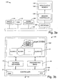
- a host or computer system 100 generally includes a system bus 104 which allows a microprocessor 108, a random access memory (RAM) 112, and input/output circuits 116 to communicate. It should be appreciated that host system 100 may generally include other components, e.g. , display devices and networking device, which are not shown for purposes of illustration.
- host system 100 may be capable of capturing information including, but not limited to, still image information, audio information, and video image information. Such information may be captured in real-time, and may be transmitted to host system 100 in a wireless manner. While host system 100 may be substantially any system, host system 100 is typically a system such as a digital camera, a video camera, a cellular communications device, an audio player, or a video player. It should be appreciated, however, that host system 100 may generally be substantially any system which stores data or information, and retrieves data or information.
- Host system 100 may also be a system which either only captures data, or only retrieves data. That is, host system 100 may be, in one embodiment, a dedicated system which stores data, or host system 100 may be a dedicated system which reads data. By way of example, host system 100 may be a memory writer which is arranged only to write or store data. Alternatively, host system 100 may be a device such as an MP3 player which is typically arranged to read or retrieve data, and not to capture data.
- a non-volatile memory device 120 which, in one embodiment, is a removable non-volatile memory device, is arranged to interface with bus 104 to store information.
- An optional interface block 130 may allow non-volatile memory device 120 to interface indirectly with bus 104.
- input/output circuit block 116 serves to reduce loading on bus 104, as will be understood by those skilled in the art.
- Non-volatile memory device 120 includes non-volatile memory 124 and an optional memory control system 128. In one embodiment, non-volatile memory device 120 may be implemented on a single chip or a die.
- non-volatile memory device 120 may be implemented on a multi-chip module, or on multiple discrete components which may form a chip set and may be used together as non-volatile memory device 120.
- One embodiment of non-volatile memory device 120 will be described below in more detail with respect to Fig. 3b.
- Non-volatile memory 124 e.g., flash memory such as NAND flash memory or an MLC NAND flash memory, is arranged to store data such that data may be accessed and read as needed. Data stored in non-volatile memory 124 may also be erased as appropriate, although it should be understood that some data in non-volatile memory 124 may not be erasable.
- the processes of storing data, reading data, and erasing data are generally controlled by memory control system 128 or, when memory control system 128 is not present, by software executed by microprocessor 108.
- the operation of non-volatile memory 124 may be managed such that the lifetime of non-volatile memory 124 is substantially maximized by essentially causing sections of non-volatile memory 124 to be worn out substantially equally.
- Non-volatile memory device 120 has generally been described as including an optional memory control system 128, i.e. , a controller. Often, non-volatile memory device 120 may include separate chips for non-volatile memory 124 and memory control system 128, i .e. , controller, functions.
- non-volatile memory devices including, but not limited to, PC cards, CompactFlash cards, MultiMedia cards, and secure digital cards include controllers which may be implemented on a separate chip, other non-volatile memory devices may not include controllers that are implemented on a separate chip.
- the memory and controller functions may be integrated into a single chip, as will be appreciated by those skilled in the art.
- the functionality of memory control system 128 may be provided by microprocessor 108, as for example in an embodiment in which non-volatile memory device 120 does not include memory controller 128, as discussed above.
- non-volatile memory device 120 includes non-volatile memory 124 and may include memory control system 128.
- Memory 124 and control system 128, or controller may be primary components of non-volatile memory device 120, although when memory 124 is an embedded NAND device such as an embedded MLC NAND memory, for example, non-volatile memory device 120 may not include control system 128.
- Memory 124 may be an array of memory cells formed on a semiconductor substrate, wherein one or more bits of data are stored in the individual memory cells by storing one of two or more levels of charge on individual storage elements of the memory cells.
- a non-volatile flash electrically erasable programmable read only memory (EEPROM) is an example of a common type of memory for such systems.
- control system 128 communicates over a bus 15 to a host computer or other system that is using the memory system to store data.
- Bus 15 is generally a part of bus 104 of Fig. 3a.
- Control system 128 also controls operation of memory 124, which may include a memory cell array 11, to write data provided by the host, read data requested by the host and perform various housekeeping functions in operating memory 124.
- Control system 128 generally includes a general purpose microprocessor which has associated non-volatile software memory, various logic circuits, and the like. One or more state machines are often also included for controlling the performance of specific routines.
- Memory cell array 11 is typically addressed by control system 128 or microprocessor 108 through address decoders 17. Decoders 17 apply the correct voltages to gate and bit lines of array 11 in order to program data to, read data from, or erase a group of memory cells being addressed by the control system 128. Additional circuits 19 include programming drivers that control voltages applied to elements of the array that depend upon the data being programmed into an addressed group of cells. Circuits 19 also include sense amplifiers and other circuits necessary to read data from an addressed group of memory cells. Data to be programmed into array 11, or data recently read from array 11, are typically stored in a buffer memory 21 within control system 128. Control system 128 also usually contains various registers for temporarily storing command and status data, and the like.
- Array 11 is divided into a large number of BLOCKS 0 - N memory cells.
- the block is typically the smallest unit of erase. That is, each block contains the minimum number of memory cells that are erased together.
- Each block is typically divided into a number of pages.
- a page may be the smallest unit of programming. That is, a basic programming operation writes data into or reads data from a minimum of one page of memory cells.
- One or more sectors of data are typically stored within each page. As shown in Fig. 3b, one sector includes user data and overhead data.
- Overhead data typically includes an ECC or other redundancy code that has been calculated from the user data of the sector.
- a portion 23 of the control system 128 calculates the ECC when data is being programmed into array 11, and also checks the ECC when data is being read from array 11. Alternatively, the ECCs are stored in different pages, or different blocks, than the user data to which they pertain.
- a sector of user data is typically 512 bytes, corresponding to the size of a sector in magnetic disk drives.
- Overhead data, or redundant data is typically an additional 16 bytes.
- One sector of data is most commonly included in each page but two or more sectors may instead form a page.
- Any number of pages may generally form a block.
- a block may be formed from eight pages up to 512, 1024 or more pages. The number of blocks is chosen to provide a desired data storage capacity for the memory system.
- Array 11 is typically divided into a few sub-arrays (not shown), each of which contains a proportion of the blocks, which operate somewhat independently of each other in order to increase the degree of parallelism in the execution of various memory operations. An example of the use of multiple sub-arrays is described in U.S. Patent No. 5,890,192.
- non-volatile memory such as an MLC NAND memory is embedded into a system, e.g. , a host system.
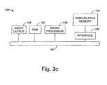
- Fig. 3c is a diagrammatic representation of a host system which includes an embedded non-volatile memory.
- a host or computer system 150 generally includes a system bus 154 which allows a microprocessor 158, a RAM 162, and input/output circuits 166, among other components (not shown) of host system 150, to communicate.
- a non-volatile memory 174 e.g., a flash memory, allows information to be stored within host system 150.
- An interface 180 may be provided between non-volatile memory 174 and bus 154 to enable information to be read from and written to non-volatile memory 174.
- Non-volatile memory 174 may be managed by microprocessor 158 which effectively executes either or both software and firmware which is arranged to control non-volatile memory 174. That is, microprocessor 158 may run code devices (not shown), i.e. , software code devices or firmware code devices, which allow non-volatile memory 174 to be controlled. Such code devices, which may be a flash memory packaged with CPU inside microprocessor 158, a separate flash ROM, or inside non-volatile memory 174, which will be described below, may enable physical blocks in non-volatile memory 174 to be addressed, and may enable information to be stored into, read from, and erased from the physical blocks.
- a page which is included in a non-volatile memory such as non-volatile 174 may be divided into segments of data which may be separately encoded using an ECC algorithm, as previously mentioned.
- the segments may be of the same size or different sizes.
- the overhead or redundant area of a page forms one segment, whereas the data area of the page may for either a single segment or a plurality of segments.
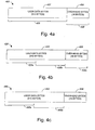
- a data section 402 which contains user data and an overhead area 404, or a redundant area may be encoded or otherwise processed substantially separately as a first segment 406 and a second segment 408. That is, a page 400 which includes data section 402 and overhead area 404 may be divided into segments 406, 408 which are encoded separately. Typically, both segments 406, 408 are encoded using substantially the same ECC algorithm, e.g. , a 1-bit ECC algorithm, although it should be appreciated that the algorithm used to encode segment 406 and the algorithm used to encode segment 408 may differ.
- a 2-bit ECC algorithm may be used to separately encode segment 406 and segment 408, thereby enabling up to two incorrect bits to be corrected within segment 406 and up to two incorrect bits to be corrected within segment 408.
- the overhead associated with implementing a 2-bit ECC algorithm is significantly higher than the overhead associated with implementing a 1-bit ECC algorithm, in order to further ensure the integrity of bytes contained in either data section 402 or overhead area 404, a 2-bit ECC algorithm may be chosen for use.
- the number of segments which are included in a page may be determined by the number of incorrect bits which a system wishes to detect and to correct. Typically, as the number of incorrect bits which are to be corrected increases, the number of segments may increased. In addition, the number of segments may also be dependent upon the number of parity bits which the system is capable of storing, as for example in an overhead area of a page. By way of example, a page may be divided into approximately three segments, although the number of segments may generally be substantially any number that is greater than or equal to two.
- Fig. 4b is a diagrammatic representation of a page which is effectively divided into three segments which may be separately encoded using an ECC algorithm in accordance with an embodiment of the present invention.
- a page 420 which includes a data section 422 and an overhead area 424 may be divided into three segments 426, 428.
- overhead area 424 is a single segment 428, while user area may be divided into segments 426a, 426b, which may be of approximately the same size, e.g. , approximately 256 bytes each when overhead area 424 is arranged to include 512 bytes.
- Each segment 426, 428 is encoded separately using an ECC algorithm.
- the ECC algorithm used to encode segments 426, 428 is a 1-bit ECC algorithm, then up to two incorrect bits in each segment 426, 428 may be detected, and one incorrect bit in each segment may be corrected. Hence, up to six incorrect bits within page 420 may be detected, while up to three incorrect bits may be corrected when a 1-bit ECC algorithm is implemented.
- the ECC algorithm used to encode segments 426, 428 allow approximately two bits in each segment 426, 428 to be corrected, while up to three incorrect bits may be corrected in each segment 426, 428.
- each segment 426, 428 is encoded using a 1-bit ECC algorithm or extended 1-bit ECC calculations, then up to three bits within page 420 may effectively be corrected using a 1-bit algorithm. Three bits may typically be corrected when incorrect bits are spread out between segment 426a, segment 426b, and segment 428. Hence, the integrity of user data stored in data section 422 and the integrity of overhead data stored in overhead area 424 may effectively be improved without incurring substantial additional overhead, since more errors within page 420 may be detected and corrected.
- a data section 442 of a page 440 may be encoded as separate segments 446 using an ECC algorithm such as a 1-bit ECC algorithm, while an overhead area 444 may not be encoded using an ECC algorithm, e.g. , may be encoded using a different algorithm.
- Separate segments 446 are generally of approximately the same size, i.e. , segment 446a and segment 446b typically each include the same number of bytes.
- Data section 442 may generally be encoded as two separate segments 446a, 446b, although the number of segments into which data section 442 may be divided may vary. By way of example, instead of being divided into two segments 446a, 446b, data section 442 may instead be divided into three segments.
- the number of parity bits which are associated with an ECC algorithm and, hence, are stored in overhead area 444 is typically approximately eight. The overhead parity bits are also stored in the overhead area. While data section 442 may generally be divided into more than three segments, the number of parity bits which are typically needed to correct data fields when data section 442 is divided into more than three segments may be too high to be readily stored into overhead area 444.
- a page 500 may include two segments 506. It should be appreciated that both segment 506a and segment 506b may both be associated with a data section or area of page 500, or segment 506a may encompass a data section of page 500 while segment 506b encompasses an overhead area of page 500.
- a 1-bit ECC algorithm is extended to encode segments 506.
- one bit in each segment 506 may be corrected using a 1-bit ECC algorithm.
- Bits within segment 506a include an incorrect bit 512a
- bits within segment 506b include an incorrect bit 512b.
- Incorrect bit 512a may be corrected to become bit 512a' within segment 506a'
- incorrect bit 512b may be corrected to become bit 512b' within segment 506b', during an error recovery process which is associated with a 1-bit ECC algorithm.
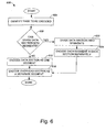
- a process 600 of encoding data begins at step 604 in which a page that is to be encoded using an ECC algorithm is identified. Once the page is identified, a determination is made in step 608 regarding whether the data section of the page is to be divided into segments. If it is determined that the data section of the page is to be divided into segments, then the data section is divided into segments in step 620.
- the number of segments associated with the data section may generally be varied. By way of example, the data section may include two segments or three segments.
- each segment in the data section may be encoded substantially separately in step 624. That is, ECC calculations, as for example ECC calculations associated with a 1-bit ECC algorithm, may be extended such that each segment created in step 620 may be encoded substantially separately.
- the overhead section is encoded as a separate segment in step 616, e.g. , using substantially the same ECC algorithm used to encode the segments associated with the data section in step 624, and the process of encoding data is completed.
- step 608 if it is determined that the data section is not to be divided into segments, then the indication is that the data section is to be encoded as a substantially single segment. Accordingly, process flow moves from step 608 to step 612 in which the data section is encoded as a single segment.
- the data section may be encoded using an ECC algorithm such as a 1-bit ECC algorithm.
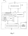
- a system architecture 700 generally includes a variety of modules which may include, but are not limited to, an application interface module 704, a system manager module 708, a data manager module 712, a data integrity manager 716, and a device manager and interface module 720.
- system architecture 700 may be implemented using software code devices or firmware which may be accessed by a processor, e.g. , processor 108 of Fig. 3a.
- application interface module 704 may be arranged to communicate with the host, operating system or the user directly.
- Application interface module 704 is also in communication with system manager module 708 and data manager module 712.
- system manager module 708 When the user wants to read, write or format a flash memory, the user sends requests to the operating system, the requests are passed to the application interface module 704.
- Application interface module 704 directs the requests to system manager module 708 or data manager module 712 depending on the requests.
- System manager module 708 includes a system initialization submodule 724, an erase count block management submodule 726, and a power management block submodule 730.
- System initialization submodule 724 is generally arranged to enable an initialization request to be processed, and typically communicates with erase count block management submodule 726.
- System initialization module 724 is also arranged to resolve a one-to-many logical-to-physical block assignment.
- Erase count block management submodule 726 includes functionality to cause erase counts of blocks to be stored, and functionality to cause an average erase count to be calculated, as well as updated, using individual erase counts. In other words, erase count block management submodule 726 effectively allows erase counts to be cataloged and allows an average erase count to be maintained. Further, in one embodiment, erase count block management submodule 726 also substantially synchronizes the erase count of substantially all blocks in an erase count block during a initialization request of an overall system. While erase count block management submodule 726 may be arranged to cause an average erase count to be stored in an erase count block, it should be appreciated that power management block submodule 730 may instead be used to enable the average erase count to be stored.
- system manager module 708 is also in communication with data manager module 712, as well as device manager and interface module 720.
- Data manager module 712 which communicates with both system manager module 708 and application interface module 704, may include functionality to provide sector mapping which effectively translates logical sectors into physical sectors. That is, data manager module 712 is arranged to map logical blocks into physical blocks.
- Data manager module 712 may also include functionality associated with operating system and file system interface layers, and enables groups within blocks to be managed, as described in co-pending U.S. Patent Application No. 10/281,855, filed October 28, 2002. In one embodiment, data manager module 712 may be arranged to enable a substantially out-of-sequence write process to occur.
- Device manager and interface module 720 which is in communication with system manager module 708, data manager 712, and data integrity manager 716, typically provides a flash memory interface, and includes functionality associated with hardware abstractions, e.g. , an I/O interface.
- Data integrity manager module 716 provides ECC handling, among other functions.
- a 1-bit ECC algorithm has been described as being suitable for use to encode contents of segments of a page substantially separately. It should be appreciated, however, that in some embodiments, other types of ECC algorithms such as a 2-bit ECC algorithm may be used to encode contents of the segments of a page substantially separately.
- Embodiments for which a 2-bit ECC algorithm may be suitable include embodiments in which a page is divided into two segments, and embodiments in which there may be ample storage space to hold parity bits associated with a 2-bit ECC algorithm.
- ECC algorithms have generally been described as being 1-bit ECC algorithms or 2-bit ECC algorithms, the ECC algorithms may instead by 1-symbol ECC algorithms or 2-symbol ECC algorithms, respectively. Further, the actual ECC algorithms used may vary widely. Suitable ECC algorithms may include, but are not limited to, Reed-Solomon algorithms, Hamming code algorithms, and binary Hamming Code algorithms. For instance, in one embodiment, a suitable 1-bit ECC algorithm which enables segments of a page to be encoded substantially separately may be a Hamming code algorithm, while a suitable 2-bit ECC algorithm may be a Reed-Solomon algorithm.
- the segments are of substantially equal size, i.e., the segments each include approximately the same number of bits. It should be appreciated, however, that the size of the segments may also vary in some instances.
- a method for encoding data associated with a page which has a data area and an overhead area within a non-volatile memory of a memory system includes dividing at least a part of the page into at least two segments of the data, the at least two segments of the data including a first segment and a second segment, and performing ECC calculations on the first segment to encode the first segment.
- the method also includes performing the ECC calculations on the second segment to encode the second segment substantially separately from the first segment.
- the present invention is related to co-pending U.S. Patent Application Nos. 10/281,739, 10/281,823, 10/281,670, 10/281,824, 10/281,631, 10/281,855, 10/281,762, 10/281,696, 10/281,626, and 10/281,804, as well as co-pending U.S. Provisional Patent Application Nos. 60/421,910, 60/421,725, 60/421,965, 60/422,166, 60/421,911, and 60/421,746, each filed on October 28, 2002, which are each incorporated herein by reference in their entireties.
Landscapes
- Engineering & Computer Science (AREA)
- Theoretical Computer Science (AREA)
- Quality & Reliability (AREA)
- Physics & Mathematics (AREA)
- General Engineering & Computer Science (AREA)
- General Physics & Mathematics (AREA)
- Techniques For Improving Reliability Of Storages (AREA)
- Detection And Correction Of Errors (AREA)
Applications Claiming Priority (2)
| Application Number | Priority Date | Filing Date | Title |
|---|---|---|---|
| US42174602P | 2002-10-28 | 2002-10-28 | |
| US421746P | 2002-10-28 |
Publications (2)
| Publication Number | Publication Date |
|---|---|
| EP1416380A2 true EP1416380A2 (fr) | 2004-05-06 |
| EP1416380A3 EP1416380A3 (fr) | 2006-04-26 |
Family
ID=32094173
Family Applications (1)
| Application Number | Title | Priority Date | Filing Date |
|---|---|---|---|
| EP03256796A Withdrawn EP1416380A3 (fr) | 2002-10-28 | 2003-10-28 | Procédé et dispositif pour la gestion de l'intégrité de données dans un système de mémoire non-volatile |
Country Status (5)
| Country | Link |
|---|---|
| US (1) | US20040083334A1 (fr) |
| EP (1) | EP1416380A3 (fr) |
| JP (1) | JP2004152300A (fr) |
| KR (1) | KR20040038709A (fr) |
| CN (1) | CN1499531A (fr) |
Cited By (3)
| Publication number | Priority date | Publication date | Assignee | Title |
|---|---|---|---|---|
| WO2007102117A3 (fr) * | 2006-03-07 | 2007-11-15 | Nxp Bv | Circuit electronique avec une matrice de memoire qui memorise des pages incluant des donnees supplementaires |
| US7843727B2 (en) | 2008-01-30 | 2010-11-30 | Samsung Electronics Co., Ltd. | Memory device and data reading method |
| US8069380B2 (en) | 2003-10-31 | 2011-11-29 | Sandisk Il Ltd. | Method, system and computer-readable code to test flash memory |
Families Citing this family (120)
| Publication number | Priority date | Publication date | Assignee | Title |
|---|---|---|---|---|
| US7559004B1 (en) | 2003-10-01 | 2009-07-07 | Sandisk Corporation | Dynamic redundant area configuration in a non-volatile memory system |
| US7099221B2 (en) | 2004-05-06 | 2006-08-29 | Micron Technology, Inc. | Memory controller method and system compensating for memory cell data losses |
| US20060010339A1 (en) * | 2004-06-24 | 2006-01-12 | Klein Dean A | Memory system and method having selective ECC during low power refresh |
| US7340668B2 (en) * | 2004-06-25 | 2008-03-04 | Micron Technology, Inc. | Low power cost-effective ECC memory system and method |
| US7116602B2 (en) | 2004-07-15 | 2006-10-03 | Micron Technology, Inc. | Method and system for controlling refresh to avoid memory cell data losses |
| US6965537B1 (en) * | 2004-08-31 | 2005-11-15 | Micron Technology, Inc. | Memory system and method using ECC to achieve low power refresh |
| EP1635261B1 (fr) * | 2004-09-10 | 2008-06-11 | STMicroelectronics S.r.l. | Mémoire avec circuit intégré gérant les codes correcteur d'erreurs |
| KR100645058B1 (ko) | 2004-11-03 | 2006-11-10 | 삼성전자주식회사 | 데이터 신뢰성을 향상시킬 수 있는 메모리 관리 기법 |
| US20060140007A1 (en) * | 2004-12-29 | 2006-06-29 | Raul-Adrian Cernea | Non-volatile memory and method with shared processing for an aggregate of read/write circuits |
| US8341371B2 (en) * | 2005-01-31 | 2012-12-25 | Sandisk Il Ltd | Method of managing copy operations in flash memories |
| US8112513B2 (en) * | 2005-11-30 | 2012-02-07 | Microsoft Corporation | Multi-user display proxy server |
| JP4791831B2 (ja) | 2006-01-20 | 2011-10-12 | 株式会社東芝 | 半導体記憶装置 |
| US8055979B2 (en) * | 2006-01-20 | 2011-11-08 | Marvell World Trade Ltd. | Flash memory with coding and signal processing |
| US7844879B2 (en) * | 2006-01-20 | 2010-11-30 | Marvell World Trade Ltd. | Method and system for error correction in flash memory |
| JP4778321B2 (ja) * | 2006-01-30 | 2011-09-21 | 富士通セミコンダクター株式会社 | 半導体メモリ、メモリシステム |
| JP4846384B2 (ja) * | 2006-02-20 | 2011-12-28 | 株式会社東芝 | 半導体記憶装置 |
| JP4836608B2 (ja) * | 2006-02-27 | 2011-12-14 | 株式会社東芝 | 半導体記憶装置 |
| US7697326B2 (en) * | 2006-05-12 | 2010-04-13 | Anobit Technologies Ltd. | Reducing programming error in memory devices |
| US8156403B2 (en) * | 2006-05-12 | 2012-04-10 | Anobit Technologies Ltd. | Combined distortion estimation and error correction coding for memory devices |
| US8239735B2 (en) * | 2006-05-12 | 2012-08-07 | Apple Inc. | Memory Device with adaptive capacity |
| CN103280239B (zh) | 2006-05-12 | 2016-04-06 | 苹果公司 | 存储设备中的失真估计和消除 |
| US7809994B2 (en) * | 2006-05-17 | 2010-10-05 | Sandisk Corporation | Error correction coding for multiple-sector pages in flash memory devices |
| US20070300130A1 (en) * | 2006-05-17 | 2007-12-27 | Sandisk Corporation | Method of Error Correction Coding for Multiple-Sector Pages in Flash Memory Devices |
| US7971071B2 (en) * | 2006-05-24 | 2011-06-28 | Walkoe Wilbur J | Integrated delivery and protection device for digital objects |
| US8060806B2 (en) | 2006-08-27 | 2011-11-15 | Anobit Technologies Ltd. | Estimation of non-linear distortion in memory devices |
| US7894289B2 (en) | 2006-10-11 | 2011-02-22 | Micron Technology, Inc. | Memory system and method using partial ECC to achieve low power refresh and fast access to data |
| US7900120B2 (en) | 2006-10-18 | 2011-03-01 | Micron Technology, Inc. | Memory system and method using ECC with flag bit to identify modified data |
| US7975192B2 (en) | 2006-10-30 | 2011-07-05 | Anobit Technologies Ltd. | Reading memory cells using multiple thresholds |
| US7821826B2 (en) | 2006-10-30 | 2010-10-26 | Anobit Technologies, Ltd. | Memory cell readout using successive approximation |
| US7924648B2 (en) | 2006-11-28 | 2011-04-12 | Anobit Technologies Ltd. | Memory power and performance management |
| WO2008068747A2 (fr) * | 2006-12-03 | 2008-06-12 | Anobit Technologies Ltd. | Gestion automatique de défauts dans des dispositifs à mémoire |
| CN101558452B (zh) * | 2006-12-07 | 2012-08-29 | Nxp股份有限公司 | 用于在闪速eeprom存储页中重构可靠性数据的方法和装置 |
| US7593263B2 (en) * | 2006-12-17 | 2009-09-22 | Anobit Technologies Ltd. | Memory device with reduced reading latency |
| US7900102B2 (en) * | 2006-12-17 | 2011-03-01 | Anobit Technologies Ltd. | High-speed programming of memory devices |
| US8583981B2 (en) * | 2006-12-29 | 2013-11-12 | Marvell World Trade Ltd. | Concatenated codes for holographic storage |
| US7751240B2 (en) | 2007-01-24 | 2010-07-06 | Anobit Technologies Ltd. | Memory device with negative thresholds |
| US8151166B2 (en) | 2007-01-24 | 2012-04-03 | Anobit Technologies Ltd. | Reduction of back pattern dependency effects in memory devices |
| US7861139B2 (en) * | 2007-01-26 | 2010-12-28 | Micron Technology, Inc. | Programming management data for NAND memories |
| WO2008111058A2 (fr) * | 2007-03-12 | 2008-09-18 | Anobit Technologies Ltd. | Estimation adaptative de seuils de lecture de cellules mémoires |
| US7904793B2 (en) * | 2007-03-29 | 2011-03-08 | Sandisk Corporation | Method for decoding data in non-volatile storage using reliability metrics based on multiple reads |
| US7797480B2 (en) * | 2007-03-29 | 2010-09-14 | Sandisk Corporation | Method for reading non-volatile storage using pre-conditioning waveforms and modified reliability metrics |
| US8001320B2 (en) | 2007-04-22 | 2011-08-16 | Anobit Technologies Ltd. | Command interface for memory devices |
| US8234545B2 (en) | 2007-05-12 | 2012-07-31 | Apple Inc. | Data storage with incremental redundancy |
| US8429493B2 (en) | 2007-05-12 | 2013-04-23 | Apple Inc. | Memory device with internal signap processing unit |
| US7925936B1 (en) | 2007-07-13 | 2011-04-12 | Anobit Technologies Ltd. | Memory device with non-uniform programming levels |
| US8259497B2 (en) | 2007-08-06 | 2012-09-04 | Apple Inc. | Programming schemes for multi-level analog memory cells |
| US8174905B2 (en) * | 2007-09-19 | 2012-05-08 | Anobit Technologies Ltd. | Programming orders for reducing distortion in arrays of multi-level analog memory cells |
| US7773413B2 (en) | 2007-10-08 | 2010-08-10 | Anobit Technologies Ltd. | Reliable data storage in analog memory cells in the presence of temperature variations |
| US8000141B1 (en) | 2007-10-19 | 2011-08-16 | Anobit Technologies Ltd. | Compensation for voltage drifts in analog memory cells |
| US8068360B2 (en) * | 2007-10-19 | 2011-11-29 | Anobit Technologies Ltd. | Reading analog memory cells using built-in multi-threshold commands |
| US8527819B2 (en) | 2007-10-19 | 2013-09-03 | Apple Inc. | Data storage in analog memory cell arrays having erase failures |
| KR101509836B1 (ko) * | 2007-11-13 | 2015-04-06 | 애플 인크. | 멀티 유닛 메모리 디바이스에서의 메모리 유닛의 최적화된 선택 |
| US8046542B2 (en) * | 2007-11-21 | 2011-10-25 | Micron Technology, Inc. | Fault-tolerant non-volatile integrated circuit memory |
| US8225181B2 (en) | 2007-11-30 | 2012-07-17 | Apple Inc. | Efficient re-read operations from memory devices |
| US8209588B2 (en) * | 2007-12-12 | 2012-06-26 | Anobit Technologies Ltd. | Efficient interference cancellation in analog memory cell arrays |
| US8456905B2 (en) | 2007-12-16 | 2013-06-04 | Apple Inc. | Efficient data storage in multi-plane memory devices |
| US8085586B2 (en) * | 2007-12-27 | 2011-12-27 | Anobit Technologies Ltd. | Wear level estimation in analog memory cells |
| US8156398B2 (en) * | 2008-02-05 | 2012-04-10 | Anobit Technologies Ltd. | Parameter estimation based on error correction code parity check equations |
| US7924587B2 (en) * | 2008-02-21 | 2011-04-12 | Anobit Technologies Ltd. | Programming of analog memory cells using a single programming pulse per state transition |
| US7864573B2 (en) | 2008-02-24 | 2011-01-04 | Anobit Technologies Ltd. | Programming analog memory cells for reduced variance after retention |
| US8230300B2 (en) * | 2008-03-07 | 2012-07-24 | Apple Inc. | Efficient readout from analog memory cells using data compression |
| US8059457B2 (en) * | 2008-03-18 | 2011-11-15 | Anobit Technologies Ltd. | Memory device with multiple-accuracy read commands |
| US8400858B2 (en) | 2008-03-18 | 2013-03-19 | Apple Inc. | Memory device with reduced sense time readout |
| JP2010009141A (ja) * | 2008-06-24 | 2010-01-14 | Toshiba Corp | データ転送方法 |
| US7995388B1 (en) | 2008-08-05 | 2011-08-09 | Anobit Technologies Ltd. | Data storage using modified voltages |
| US7924613B1 (en) | 2008-08-05 | 2011-04-12 | Anobit Technologies Ltd. | Data storage in analog memory cells with protection against programming interruption |
| CN101650974B (zh) * | 2008-08-12 | 2012-12-19 | 创见资讯股份有限公司 | 可自我检测使用状态的储存装置及其检测方法 |
| US8949684B1 (en) | 2008-09-02 | 2015-02-03 | Apple Inc. | Segmented data storage |
| US8169825B1 (en) | 2008-09-02 | 2012-05-01 | Anobit Technologies Ltd. | Reliable data storage in analog memory cells subjected to long retention periods |
| US8482978B1 (en) | 2008-09-14 | 2013-07-09 | Apple Inc. | Estimation of memory cell read thresholds by sampling inside programming level distribution intervals |
| US8000135B1 (en) | 2008-09-14 | 2011-08-16 | Anobit Technologies Ltd. | Estimation of memory cell read thresholds by sampling inside programming level distribution intervals |
| US8239734B1 (en) | 2008-10-15 | 2012-08-07 | Apple Inc. | Efficient data storage in storage device arrays |
| US8261159B1 (en) | 2008-10-30 | 2012-09-04 | Apple, Inc. | Data scrambling schemes for memory devices |
| US8208304B2 (en) * | 2008-11-16 | 2012-06-26 | Anobit Technologies Ltd. | Storage at M bits/cell density in N bits/cell analog memory cell devices, M>N |
| US8473815B2 (en) * | 2008-12-22 | 2013-06-25 | Industrial Technology Research Institute | Methods and systems of a flash memory controller and an error correction code (ECC) controller using variable-length segmented ECC data |
| US8248831B2 (en) * | 2008-12-31 | 2012-08-21 | Apple Inc. | Rejuvenation of analog memory cells |
| US8174857B1 (en) | 2008-12-31 | 2012-05-08 | Anobit Technologies Ltd. | Efficient readout schemes for analog memory cell devices using multiple read threshold sets |
| US8924661B1 (en) | 2009-01-18 | 2014-12-30 | Apple Inc. | Memory system including a controller and processors associated with memory devices |
| US8228701B2 (en) | 2009-03-01 | 2012-07-24 | Apple Inc. | Selective activation of programming schemes in analog memory cell arrays |
| US8259506B1 (en) | 2009-03-25 | 2012-09-04 | Apple Inc. | Database of memory read thresholds |
| US8832354B2 (en) * | 2009-03-25 | 2014-09-09 | Apple Inc. | Use of host system resources by memory controller |
| US8238157B1 (en) | 2009-04-12 | 2012-08-07 | Apple Inc. | Selective re-programming of analog memory cells |
| US8438453B2 (en) * | 2009-05-06 | 2013-05-07 | Apple Inc. | Low latency read operation for managed non-volatile memory |
| US8479080B1 (en) | 2009-07-12 | 2013-07-02 | Apple Inc. | Adaptive over-provisioning in memory systems |
| US20110041005A1 (en) * | 2009-08-11 | 2011-02-17 | Selinger Robert D | Controller and Method for Providing Read Status and Spare Block Management Information in a Flash Memory System |
| US20110041039A1 (en) * | 2009-08-11 | 2011-02-17 | Eliyahou Harari | Controller and Method for Interfacing Between a Host Controller in a Host and a Flash Memory Device |
| US8615700B2 (en) * | 2009-08-18 | 2013-12-24 | Viasat, Inc. | Forward error correction with parallel error detection for flash memories |
| CN102004701B (zh) * | 2009-08-28 | 2013-01-09 | 炬才微电子(深圳)有限公司 | 一种次级内存的分配方法和装置 |
| US8495465B1 (en) | 2009-10-15 | 2013-07-23 | Apple Inc. | Error correction coding over multiple memory pages |
| US8677054B1 (en) | 2009-12-16 | 2014-03-18 | Apple Inc. | Memory management schemes for non-volatile memory devices |
| US8694814B1 (en) | 2010-01-10 | 2014-04-08 | Apple Inc. | Reuse of host hibernation storage space by memory controller |
| US8572311B1 (en) | 2010-01-11 | 2013-10-29 | Apple Inc. | Redundant data storage in multi-die memory systems |
| US8694853B1 (en) | 2010-05-04 | 2014-04-08 | Apple Inc. | Read commands for reading interfering memory cells |
| US8572423B1 (en) | 2010-06-22 | 2013-10-29 | Apple Inc. | Reducing peak current in memory systems |
| US8595591B1 (en) | 2010-07-11 | 2013-11-26 | Apple Inc. | Interference-aware assignment of programming levels in analog memory cells |
| US9104580B1 (en) | 2010-07-27 | 2015-08-11 | Apple Inc. | Cache memory for hybrid disk drives |
| US8645794B1 (en) | 2010-07-31 | 2014-02-04 | Apple Inc. | Data storage in analog memory cells using a non-integer number of bits per cell |
| US8856475B1 (en) | 2010-08-01 | 2014-10-07 | Apple Inc. | Efficient selection of memory blocks for compaction |
| US8694854B1 (en) | 2010-08-17 | 2014-04-08 | Apple Inc. | Read threshold setting based on soft readout statistics |
| CN101957767A (zh) * | 2010-09-21 | 2011-01-26 | 深圳创维数字技术股份有限公司 | 基于与非型闪存存储设备的系统软件升级方法 |
| US9021181B1 (en) | 2010-09-27 | 2015-04-28 | Apple Inc. | Memory management for unifying memory cell conditions by using maximum time intervals |
| JP2012094132A (ja) * | 2010-10-01 | 2012-05-17 | Siglead Inc | 不揮発性半導体メモリ装置とデータ誤り訂正方法 |
| KR101861247B1 (ko) * | 2011-04-06 | 2018-05-28 | 삼성전자주식회사 | 메모리 컨트롤러, 이의 데이터 처리 방법, 및 이를 포함하는 메모리 시스템 |
| US8910017B2 (en) | 2012-07-02 | 2014-12-09 | Sandisk Technologies Inc. | Flash memory with random partition |
| KR102081980B1 (ko) | 2012-10-08 | 2020-02-27 | 삼성전자 주식회사 | 메모리 시스템에서의 라이트 동작 또는 리드 동작 수행 방법 |
| US9146809B2 (en) | 2013-10-07 | 2015-09-29 | Macronix International Co., Ltd. | ECC method for double pattern flash memory |
| US9535785B2 (en) | 2014-01-17 | 2017-01-03 | Macronix International Co., Ltd. | ECC method for flash memory |
| US10223197B2 (en) * | 2015-08-06 | 2019-03-05 | Nxp B.V. | Integrated circuit device and method for applying error correction to SRAM memory |
| US9778983B2 (en) | 2015-08-06 | 2017-10-03 | Nxp B.V. | Integrated circuit device and method for reducing SRAM leakage |
| US10437666B2 (en) | 2015-08-06 | 2019-10-08 | Nxp B.V. | Integrated circuit device and method for reading data from an SRAM memory |
| US10304550B1 (en) | 2017-11-29 | 2019-05-28 | Sandisk Technologies Llc | Sense amplifier with negative threshold sensing for non-volatile memory |
| CN108418589B (zh) * | 2018-03-05 | 2020-07-10 | 华中科技大学 | 一种单层非易失存储器的动态编解码方法 |
| KR102076624B1 (ko) * | 2018-12-06 | 2020-02-12 | 한국외국어대학교 연구산학협력단 | 플래시 메모리 기반의 저장 시스템 및 이의 에러 보정 방법 |
| US10643695B1 (en) | 2019-01-10 | 2020-05-05 | Sandisk Technologies Llc | Concurrent multi-state program verify for non-volatile memory |
| US11024392B1 (en) | 2019-12-23 | 2021-06-01 | Sandisk Technologies Llc | Sense amplifier for bidirectional sensing of memory cells of a non-volatile memory |
| US11468963B2 (en) * | 2020-12-08 | 2022-10-11 | Macronix International Co., Ltd. | Memory device and read method thereof |
| US11455254B2 (en) * | 2020-12-10 | 2022-09-27 | Macronix International Co., Ltd. | Flash memory system and flash memory device thereof |
| US11556416B2 (en) | 2021-05-05 | 2023-01-17 | Apple Inc. | Controlling memory readout reliability and throughput by adjusting distance between read thresholds |
| US11847342B2 (en) | 2021-07-28 | 2023-12-19 | Apple Inc. | Efficient transfer of hard data and confidence levels in reading a nonvolatile memory |
| US12057167B2 (en) | 2022-08-28 | 2024-08-06 | Micron Technology, Inc. | Padding in flash memory blocks |
Family Cites Families (37)
| Publication number | Priority date | Publication date | Assignee | Title |
|---|---|---|---|---|
| US5268870A (en) * | 1988-06-08 | 1993-12-07 | Eliyahou Harari | Flash EEPROM system and intelligent programming and erasing methods therefor |
| DE69024086T2 (de) * | 1989-04-13 | 1996-06-20 | Sundisk Corp | EEprom-System mit Blocklöschung |
| US5164944A (en) * | 1990-06-08 | 1992-11-17 | Unisys Corporation | Method and apparatus for effecting multiple error correction in a computer memory |
| US5222109A (en) * | 1990-12-28 | 1993-06-22 | Ibm Corporation | Endurance management for solid state files |
| US5438573A (en) * | 1991-09-13 | 1995-08-01 | Sundisk Corporation | Flash EEPROM array data and header file structure |
| US6230233B1 (en) * | 1991-09-13 | 2001-05-08 | Sandisk Corporation | Wear leveling techniques for flash EEPROM systems |
| JP2856621B2 (ja) * | 1993-02-24 | 1999-02-10 | インターナショナル・ビジネス・マシーンズ・コーポレイション | 一括消去型不揮発性メモリおよびそれを用いる半導体ディスク装置 |
| US5388083A (en) * | 1993-03-26 | 1995-02-07 | Cirrus Logic, Inc. | Flash memory mass storage architecture |
| US5603001A (en) * | 1994-05-09 | 1997-02-11 | Kabushiki Kaisha Toshiba | Semiconductor disk system having a plurality of flash memories |
| US5509119A (en) * | 1994-09-23 | 1996-04-16 | Hewlett-Packard Company | Fast comparison method and apparatus for error corrected cache tags |
| US5666371A (en) * | 1995-02-24 | 1997-09-09 | Unisys Corporation | Method and apparatus for detecting errors in a system that employs multi-bit wide memory elements |
| US5845313A (en) * | 1995-07-31 | 1998-12-01 | Lexar | Direct logical block addressing flash memory mass storage architecture |
| US5907856A (en) * | 1995-07-31 | 1999-05-25 | Lexar Media, Inc. | Moving sectors within a block of information in a flash memory mass storage architecture |
| JP3604466B2 (ja) * | 1995-09-13 | 2004-12-22 | 株式会社ルネサステクノロジ | フラッシュディスクカード |
| US6125435A (en) * | 1995-09-13 | 2000-09-26 | Lexar Media, Inc. | Alignment of cluster address to block addresses within a semiconductor non-volatile mass storage memory |
| US5835935A (en) * | 1995-09-13 | 1998-11-10 | Lexar Media, Inc. | Method of and architecture for controlling system data with automatic wear leveling in a semiconductor non-volatile mass storage memory |
| US5860082A (en) * | 1996-03-28 | 1999-01-12 | Datalight, Inc. | Method and apparatus for allocating storage in a flash memory |
| JPH10207726A (ja) * | 1997-01-23 | 1998-08-07 | Oki Electric Ind Co Ltd | 半導体ディスク装置 |
| US5896404A (en) * | 1997-04-04 | 1999-04-20 | International Business Machines Corporation | Programmable burst length DRAM |
| US6182239B1 (en) * | 1998-02-06 | 2001-01-30 | Stmicroelectronics, Inc. | Fault-tolerant codes for multi-level memories |
| KR100297986B1 (ko) * | 1998-03-13 | 2001-10-25 | 김영환 | 플래쉬 메모리 셀 어레이의 웨어 레벨링 시스템 및 웨어 레벨링 방법 |
| KR100287018B1 (ko) * | 1998-08-07 | 2001-04-16 | 윤종용 | 에러 정정 회로를 구비한 반도체 메모리 장치 |
| US6260156B1 (en) * | 1998-12-04 | 2001-07-10 | Datalight, Inc. | Method and system for managing bad areas in flash memory |
| JP2000173289A (ja) * | 1998-12-10 | 2000-06-23 | Toshiba Corp | エラー訂正可能なフラッシュメモリシステム |
| US6041001A (en) * | 1999-02-25 | 2000-03-21 | Lexar Media, Inc. | Method of increasing data reliability of a flash memory device without compromising compatibility |
| US6353910B1 (en) * | 1999-04-09 | 2002-03-05 | International Business Machines Corporation | Method and apparatus for implementing error correction coding (ECC) in a dynamic random access memory utilizing vertical ECC storage |
| JP3975245B2 (ja) * | 1999-12-16 | 2007-09-12 | 株式会社ルネサステクノロジ | 記録再生装置および半導体メモリ |
| US6662333B1 (en) * | 2000-02-04 | 2003-12-09 | Hewlett-Packard Development Company, L.P. | Shared error correction for memory design |
| US6426893B1 (en) * | 2000-02-17 | 2002-07-30 | Sandisk Corporation | Flash eeprom system with simultaneous multiple data sector programming and storage of physical block characteristics in other designated blocks |
| US6747827B1 (en) * | 2000-03-27 | 2004-06-08 | Texas Instruments Incorporated | Error correction codes applied variably by disk zone, track, sector, or content |
| JP2001297038A (ja) * | 2000-04-11 | 2001-10-26 | Toshiba Corp | データ記憶装置および記録媒体並びに記録媒体制御方法 |
| US6941505B2 (en) * | 2000-09-12 | 2005-09-06 | Hitachi, Ltd. | Data processing system and data processing method |
| US6961890B2 (en) * | 2001-08-16 | 2005-11-01 | Hewlett-Packard Development Company, L.P. | Dynamic variable-length error correction code |
| US6948026B2 (en) * | 2001-08-24 | 2005-09-20 | Micron Technology, Inc. | Erase block management |
| GB0123419D0 (en) * | 2001-09-28 | 2001-11-21 | Memquest Ltd | Data handling system |
| GB0123422D0 (en) * | 2001-09-28 | 2001-11-21 | Memquest Ltd | Improved memory controller |
| US8412879B2 (en) * | 2002-10-28 | 2013-04-02 | Sandisk Technologies Inc. | Hybrid implementation for error correction codes within a non-volatile memory system |
-
2003
- 2003-10-02 US US10/679,000 patent/US20040083334A1/en not_active Abandoned
- 2003-10-27 KR KR1020030075138A patent/KR20040038709A/ko not_active Withdrawn
- 2003-10-28 CN CNA2003101046447A patent/CN1499531A/zh active Pending
- 2003-10-28 JP JP2003368139A patent/JP2004152300A/ja active Pending
- 2003-10-28 EP EP03256796A patent/EP1416380A3/fr not_active Withdrawn
Cited By (5)
| Publication number | Priority date | Publication date | Assignee | Title |
|---|---|---|---|---|
| US8069380B2 (en) | 2003-10-31 | 2011-11-29 | Sandisk Il Ltd. | Method, system and computer-readable code to test flash memory |
| WO2007102117A3 (fr) * | 2006-03-07 | 2007-11-15 | Nxp Bv | Circuit electronique avec une matrice de memoire qui memorise des pages incluant des donnees supplementaires |
| US7913110B2 (en) | 2006-03-07 | 2011-03-22 | Nxp B.V. | Electronic circuit with a memory matrix that stores pages including extra data |
| CN101395583B (zh) * | 2006-03-07 | 2011-03-23 | Nxp股份有限公司 | 具有存储着包含附加数据在内的页面的存储矩阵的电子电路 |
| US7843727B2 (en) | 2008-01-30 | 2010-11-30 | Samsung Electronics Co., Ltd. | Memory device and data reading method |
Also Published As
| Publication number | Publication date |
|---|---|
| CN1499531A (zh) | 2004-05-26 |
| EP1416380A3 (fr) | 2006-04-26 |
| JP2004152300A (ja) | 2004-05-27 |
| US20040083334A1 (en) | 2004-04-29 |
| KR20040038709A (ko) | 2004-05-08 |
Similar Documents
| Publication | Publication Date | Title |
|---|---|---|
| EP1416380A2 (fr) | Procédé et dispositif pour la gestion de l'intégrité de données dans un système de mémoire non-volatile | |
| US7559004B1 (en) | Dynamic redundant area configuration in a non-volatile memory system | |
| US8412879B2 (en) | Hybrid implementation for error correction codes within a non-volatile memory system | |
| US7032087B1 (en) | Erase count differential table within a non-volatile memory system | |
| US7702880B2 (en) | Hybrid mapping implementation within a non-volatile memory system | |
| US7526599B2 (en) | Method and apparatus for effectively enabling an out of sequence write process within a non-volatile memory system | |
| CN106598479B (zh) | 闪速存储器的故障安全擦除的方法和装置 | |
| US7246268B2 (en) | Method and apparatus for dynamic degradation detection | |
| KR101004876B1 (ko) | 비휘발성 메모리 시스템에서 사용하기 위한 전원 관리 블록 | |
| US7089349B2 (en) | Internal maintenance schedule request for non-volatile memory system | |
| US8635510B2 (en) | Non-systematic coded error correction | |
| US20160070507A1 (en) | Memory system and method of controlling memory device | |
| US9812194B1 (en) | Decoding method, memory storage device and memory control circuit unit | |
| US11101822B1 (en) | Data writing method, memory control circuit unit and memory storage apparatus | |
| US20170052704A1 (en) | Memory management method, memory control circuit unit and memory storage device | |
| US8706990B2 (en) | Adaptive internal table backup for non-volatile memory system | |
| US9383929B2 (en) | Data storing method and memory controller and memory storage device using the same | |
| US7234036B1 (en) | Method and apparatus for resolving physical blocks associated with a common logical block | |
| US8533549B2 (en) | Memory system and computer system | |
| CN103218308A (zh) | 缓冲存储器管理方法、存储器控制器与存储器储存装置 | |
| US10824368B2 (en) | Data storing method, memory control circuit unit and memory storage device | |
| US11604586B2 (en) | Data protection method, with disk array tags, memory storage device and memory control circuit unit | |
| CN120104055B (zh) | 读取方法、存储器存储装置与存储器控制电路单元 | |
| US11430538B1 (en) | Memory control method, memory storage device, and memory control circuit unit |
Legal Events
| Date | Code | Title | Description |
|---|---|---|---|
| PUAI | Public reference made under article 153(3) epc to a published international application that has entered the european phase |
Free format text: ORIGINAL CODE: 0009012 |
|
| AK | Designated contracting states |
Kind code of ref document: A2 Designated state(s): AT BE BG CH CY CZ DE DK EE ES FI FR GB GR HU IE IT LI LU MC NL PT RO SE SI SK TR |
|
| AX | Request for extension of the european patent |
Extension state: AL LT LV MK |
|
| PUAL | Search report despatched |
Free format text: ORIGINAL CODE: 0009013 |
|
| AK | Designated contracting states |
Kind code of ref document: A3 Designated state(s): AT BE BG CH CY CZ DE DK EE ES FI FR GB GR HU IE IT LI LU MC NL PT RO SE SI SK TR |
|
| AX | Request for extension of the european patent |
Extension state: AL LT LV MK |
|
| 17P | Request for examination filed |
Effective date: 20061018 |
|
| AKX | Designation fees paid |
Designated state(s): AT BE BG CH CY CZ DE DK EE ES FI FR GB GR HU IE IT LI LU MC NL PT RO SE SI SK TR |
|
| STAA | Information on the status of an ep patent application or granted ep patent |
Free format text: STATUS: THE APPLICATION IS DEEMED TO BE WITHDRAWN |
|
| 18D | Application deemed to be withdrawn |
Effective date: 20090501 |