EP1417829B1 - Dispositif d'enregistrement d'images avec transition amelioree du stockage d'images - Google Patents
Dispositif d'enregistrement d'images avec transition amelioree du stockage d'images Download PDFInfo
- Publication number
- EP1417829B1 EP1417829B1 EP02751534A EP02751534A EP1417829B1 EP 1417829 B1 EP1417829 B1 EP 1417829B1 EP 02751534 A EP02751534 A EP 02751534A EP 02751534 A EP02751534 A EP 02751534A EP 1417829 B1 EP1417829 B1 EP 1417829B1
- Authority
- EP
- European Patent Office
- Prior art keywords
- gates
- transition region
- image
- recording device
- section
- Prior art date
- Legal status (The legal status is an assumption and is not a legal conclusion. Google has not performed a legal analysis and makes no representation as to the accuracy of the status listed.)
- Expired - Lifetime
Links
- 230000007704 transition Effects 0.000 title claims abstract description 35
- 239000000758 substrate Substances 0.000 description 6
- 238000010586 diagram Methods 0.000 description 3
- 230000004888 barrier function Effects 0.000 description 2
- 229910021420 polycrystalline silicon Inorganic materials 0.000 description 2
- 230000000903 blocking effect Effects 0.000 description 1
- 230000000694 effects Effects 0.000 description 1
- 230000037433 frameshift Effects 0.000 description 1
- 239000007943 implant Substances 0.000 description 1
- 230000006872 improvement Effects 0.000 description 1
- 239000012528 membrane Substances 0.000 description 1
- 238000012986 modification Methods 0.000 description 1
- 230000004048 modification Effects 0.000 description 1
- 230000000149 penetrating effect Effects 0.000 description 1
- 230000002572 peristaltic effect Effects 0.000 description 1
- 229920005591 polysilicon Polymers 0.000 description 1
- 230000000717 retained effect Effects 0.000 description 1
- 238000012216 screening Methods 0.000 description 1
- 238000000926 separation method Methods 0.000 description 1
- 238000004088 simulation Methods 0.000 description 1
Images


Classifications
-
- H—ELECTRICITY
- H04—ELECTRIC COMMUNICATION TECHNIQUE
- H04N—PICTORIAL COMMUNICATION, e.g. TELEVISION
- H04N1/00—Scanning, transmission or reproduction of documents or the like, e.g. facsimile transmission; Details thereof
- H04N1/04—Scanning arrangements, i.e. arrangements for the displacement of active reading or reproducing elements relative to the original or reproducing medium, or vice versa
- H04N1/19—Scanning arrangements, i.e. arrangements for the displacement of active reading or reproducing elements relative to the original or reproducing medium, or vice versa using multi-element arrays
-
- H—ELECTRICITY
- H10—SEMICONDUCTOR DEVICES; ELECTRIC SOLID-STATE DEVICES NOT OTHERWISE PROVIDED FOR
- H10F—INORGANIC SEMICONDUCTOR DEVICES SENSITIVE TO INFRARED RADIATION, LIGHT, ELECTROMAGNETIC RADIATION OF SHORTER WAVELENGTH OR CORPUSCULAR RADIATION
- H10F39/00—Integrated devices, or assemblies of multiple devices, comprising at least one element covered by group H10F30/00, e.g. radiation detectors comprising photodiode arrays
- H10F39/10—Integrated devices
- H10F39/12—Image sensors
- H10F39/18—Complementary metal-oxide-semiconductor [CMOS] image sensors; Photodiode array image sensors
- H10F39/189—X-ray, gamma-ray or corpuscular radiation imagers
Definitions
- An image recording device for application as a so-called 'Digital Still Camera' is often provided with an FT-CCD (Frame Transfer-Charge Coupled Device) and usually requires a real-time preview mode, for example for an electronic viewfmder such as an LCD screen, a display on a television in accordance with the NTSC or PAL standard, or for camera functions such as horizontal and vertical automatic focusing.
- FT-CCD Full Transfer-Charge Coupled Device
- the invention relates to such an image recording device, comprising:
- Such an FT-CCD with a storage section of limited size is known, for example, from the international patent application WO 98/17051 ( PCT/IB97/01201 ) that has been published on 23 April 1998.
- WO 98/17051 PCT/IB97/01201
- the speed hereof is in need of improvement, while the further performance of the sensor, such as a high maximum charge value Qmax and a high frame shift frequency, must be retained and charge overflow must be avoided.
- an image-recording device of the kind mentioned in the opening paragraph is characterized that one or more gates in the transition region have a larger length than the gates outside the transition region.
- the doping concentration below one or more gates in the transition region is modified with respect to the doping below the gates outside the transition region.
- An image recording device 10 ( Fig. 1 ) comprises a recording part 11 and a storage part 12, with a transition 13, diagrammatically indicated with a broken line, between the parts 11 and 12. Furthermore, a so-called horizontal read-out register 14 is connected to the recording part.
- FIG. 2 The diagrammatic view of Fig. 2 further shows vertical channels 23 along which the charge can be transported from the recording part 11 to the storage part 12 in the direction of an arrow A.
- Four-phase driven electrodes A1 to A4 for gates arranged above channels 23 in the image recording area are connected to clock lines 24, 25, 26, and 27, respectively, while electrodes B1 to B4 in the storage area are connected to clock lines 28, 29, 30, 31, respectively.
- Clock lines 24 to 31 are driven from a diagrammatically indicated clock driving circuit 32.
- the present embodiment relates to a four-phase image recording device.
- the recording part 11 comprises 1280 horizontal lines and 960 vertical channels, wherein the electrodes A1 to A4 are repeated in each case.
- the storage part 12 then has a smaller capacity of for instance 240 lines by 960 vertical channels, i.e. a notably smaller number of lines than the image recording part.
- electrodes A1, A2, A3, A4, B1, B2, B3 B4, B1 forming the gates are arranged close to the transition 13 on an insulating layer 34 on the channels 23, under which a p-type layer 35 is provided on a substrate 36 which is brought to the desired voltage by a voltage source 37.
- a diagrammatically indicated light-screening layer 38 which prevents light from penetrating into the storage part 12 and which is preferably integrated into the circuit in a manner not shown.
- the gates A2, A3, A4, A1, A2, A3, A4, B1, B2, B3, B4, B1 close to the transition 13 have the following lengths:
- the p-well at the transition was lower-doped, in the present embodiment by narrowing the implementation width under the last two image electrodes to 1.6 ⁇ m, as opposed to 2.4 ⁇ m at the other gates.
- the diagram of Fig. 4B shows the drive diagram in subsampling, wherein the surplus charge must be drained to the substrate at the third clock cycle and lateral leakage thereof must be avoided.
- the maximum charge capacity amounts to, for example, only 30,000 electrons, whereas that at step t4 it is no more than 25,000 electrons.
- the surplus must also be drained rapidly to the substrate at clock cycle t4.
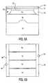
- a four-phase pixel of Fig. 5A (shown in cross-section) and 5B (shown in plan view), in which the longer gates close to the transition in accordance with the above description are preferably used, further details of which are described in the article by H. Peek et al. 'An FT-CCD image with true 2.4 x 2.4 ⁇ m 2 pixels in double membrane poly-Si technology' (IEDM 1996 pp. 35.3.1-4)
- four gates with a length of 0.9 ⁇ m of polysilicon 52 are each situated on an insulating layer 51, while an n-channel 53 extends between two stop areas 54.
- a so-called profiled peristaltic implant 55 for enlarging the well, i.e. the charge capacity, is situated between the oxide layer and the n-channel, while a p-well 56 is situated on the n-substrate 57 under the n-channel 53.
Landscapes
- Engineering & Computer Science (AREA)
- Multimedia (AREA)
- Signal Processing (AREA)
- Solid State Image Pick-Up Elements (AREA)
Abstract
Claims (7)
- Dispositif d'enregistrement d'images (10), comprenant :- une section d'image (11) avec des grilles (Ai) et une pluralité d'éléments d'image (pixels) agencés en rangées et colonnes ;- une section de stockage (12) avec des grilles (Bi) et des éléments de stockage d'image agencés en rangées et colonnes pour stocker au moins partiellement (temporairement) une charge absorbée par les pixels, dans lequel la charge est transférée aux éléments de stockage ;- une transition (13) qui est présente entre la section d'image (11) et la section de stockage (12) et une région de transition qui comprend la transition (13) et des parties de la section d'image (11) et de la section de stockage (12), et dans lequel les grilles (Ai,Bi) de la section d'image (11) et de la section de stockage (12) en dehors de la région de transition ont substantiellement la même longueur,caractérisé en ce que une ou plusieurs des grilles (A1,A2,A3,A4,B1,B2,B3,B4) dans la région de transition ont une longueur plus grande que les grilles en dehors de la région de transition.
- Dispositif d'enregistrement d'images selon la revendication 1, caractérisé en ce que les deux premières grilles (B1,B2) dans la partie de la région de transition faisant partie de la section de stockage (12) ont une longueur qui est 50% plus grande que la longueur des grilles (Bi) de la section de stockage (12) en dehors de la régions de transition.
- Dispositif d'enregistrement d'images selon la revendication 1 ou 2, caractérisé en ce que la seconde grille d'une partie de la région de transition faisant partie de la section d'image (11), vue depuis la transition (13), a une longueur d'approximativement 2,5 à 3 fois la longueur d'une grilles (Ai) de la section d'image (11) en dehors de la région de transition.
- Dispositif d'enregistrement d'images selon une quelconque des revendications précédentes, caractérisé en ce que le dopage en dessous d'une ou plusieurs grilles (A4,A3,B1,B2) dans la région de transition est modifié par rapport au dopage en dessous des grilles (Ai,Bi) en dehors de la région de transition.
- Dispositif d'enregistrement d'images selon la revendication 4, caractérisé en ce que, pendant le fonctionnement du dispositif, le potentiel de canal obtenu sous une ou plusieurs grilles (A4,A3,B1,B2) dans la région de transition est plus grand que celui obtenu en dessous des grilles (Ai,Bi) en dehors de la région de transition.
- Dispositif d'enregistrement d'images selon la revendication 4 ou 5, caractérisé en ce que le dopage modifié implique que la concentration de dopage en dessous de la ou des grilles (A4,A3,B1,B2) dans la région de transition soit inférieure à la concentration de dopage en dessous des grilles (Ai,Bi) en dehors de la région de transition.
- Dispositif d'enregistrement d'images selon la revendication 4 ou 6, caractérisé en ce que le dopage modifié est caractérisé par une concentration de dopage plus basse constituée par un dopage diminué.
Priority Applications (1)
| Application Number | Priority Date | Filing Date | Title |
|---|---|---|---|
| EP02751534A EP1417829B1 (fr) | 2001-08-02 | 2002-07-17 | Dispositif d'enregistrement d'images avec transition amelioree du stockage d'images |
Applications Claiming Priority (4)
| Application Number | Priority Date | Filing Date | Title |
|---|---|---|---|
| EP01202927 | 2001-08-02 | ||
| EP01202927 | 2001-08-02 | ||
| EP02751534A EP1417829B1 (fr) | 2001-08-02 | 2002-07-17 | Dispositif d'enregistrement d'images avec transition amelioree du stockage d'images |
| PCT/IB2002/003107 WO2003013126A1 (fr) | 2001-08-02 | 2002-07-17 | Dispositif d'enregistrement d'images avec transition amelioree du stockage d'images |
Publications (2)
| Publication Number | Publication Date |
|---|---|
| EP1417829A1 EP1417829A1 (fr) | 2004-05-12 |
| EP1417829B1 true EP1417829B1 (fr) | 2009-04-08 |
Family
ID=8180740
Family Applications (1)
| Application Number | Title | Priority Date | Filing Date |
|---|---|---|---|
| EP02751534A Expired - Lifetime EP1417829B1 (fr) | 2001-08-02 | 2002-07-17 | Dispositif d'enregistrement d'images avec transition amelioree du stockage d'images |
Country Status (4)
| Country | Link |
|---|---|
| US (1) | US6747701B2 (fr) |
| EP (1) | EP1417829B1 (fr) |
| DE (1) | DE60231882D1 (fr) |
| WO (1) | WO2003013126A1 (fr) |
Families Citing this family (1)
| Publication number | Priority date | Publication date | Assignee | Title |
|---|---|---|---|---|
| WO2002104007A2 (fr) * | 2001-06-15 | 2002-12-27 | Dalsa Corporation | Dispositif de prise d'image et camera associee |
Family Cites Families (8)
| Publication number | Priority date | Publication date | Assignee | Title |
|---|---|---|---|---|
| EP0244655B1 (fr) * | 1986-04-07 | 1994-08-10 | Fuji Photo Film Co., Ltd. | Appareil de prise de vue couleur à l'état solide |
| DE69120773T2 (de) * | 1990-11-09 | 1997-02-06 | Matsushita Electronics Corp | Ladungsträgeranordnung, Verfahren zu ihrer Herstellung und Verfahren zu ihrer Steuerung |
| JP3160382B2 (ja) * | 1992-08-27 | 2001-04-25 | 株式会社東芝 | 固体撮像装置 |
| JPH08242410A (ja) * | 1994-12-30 | 1996-09-17 | Eastman Kodak Co | 電子カメラの順次走査センサからインタレースされた画像を作成する電子カメラ |
| JP3703175B2 (ja) * | 1995-07-31 | 2005-10-05 | キヤノン株式会社 | 撮像装置 |
| US6654059B1 (en) * | 1996-10-03 | 2003-11-25 | Dalsa Corporation | Charge coupled imaging device and method in which redundant lines can be dumped |
| JP2002517136A (ja) * | 1998-05-26 | 2002-06-11 | コーニンクレッカ フィリップス エレクトロニクス エヌ ヴィ | 固体撮像装置 |
| US6331873B1 (en) * | 1998-12-03 | 2001-12-18 | Massachusetts Institute Of Technology | High-precision blooming control structure formation for an image sensor |
-
2002
- 2002-07-17 DE DE60231882T patent/DE60231882D1/de not_active Expired - Lifetime
- 2002-07-17 WO PCT/IB2002/003107 patent/WO2003013126A1/fr not_active Ceased
- 2002-07-17 EP EP02751534A patent/EP1417829B1/fr not_active Expired - Lifetime
- 2002-07-30 US US10/208,672 patent/US6747701B2/en not_active Expired - Lifetime
Also Published As
| Publication number | Publication date |
|---|---|
| EP1417829A1 (fr) | 2004-05-12 |
| DE60231882D1 (de) | 2009-05-20 |
| US20030025819A1 (en) | 2003-02-06 |
| WO2003013126A1 (fr) | 2003-02-13 |
| US6747701B2 (en) | 2004-06-08 |
Similar Documents
| Publication | Publication Date | Title |
|---|---|---|
| US7053948B2 (en) | Solid-state image pickup device with discharge gate operable in an arbitrary timing | |
| US5896172A (en) | Method of operating a CCD imager suitable for the implementation of such a method | |
| US7002630B1 (en) | Method of driving solid-state imaging device, solid-state imaging device and camera | |
| KR960002643B1 (ko) | 고체 촬상 소자 | |
| EP0732748B1 (fr) | Capteur d'images à état solide et méthode de commande | |
| US6243135B1 (en) | Solid state imaging device having overflow drain region | |
| EP0712237B1 (fr) | Méthode de commande d'un dispositif CCD de prise d'images à l'état solide et caméra vidéo l'employant | |
| EP0403939A2 (fr) | Méthode de commande d'un capteur d'image à l'état solide | |
| US6654059B1 (en) | Charge coupled imaging device and method in which redundant lines can be dumped | |
| JP2001326344A (ja) | Lodブルーミング抑圧構造を備えるフル・フレーム型イメージセンサ用高速掃き出し構造 | |
| EP0547697A2 (fr) | Dispositif de prise de vues à l'état solide et caméra munie d'un tel dispositif de prise de vues | |
| JPH05283666A (ja) | 固体撮像素子 | |
| JP2845216B2 (ja) | 固体撮像装置およびその製造方法 | |
| JPH02309877A (ja) | 固体撮像装置 | |
| US6760073B1 (en) | Solid-state image sensor | |
| US6747701B2 (en) | Image recording device with improved image storage transition | |
| EP0668691B1 (fr) | Dispositif capteur d'images à couplage de charges et caméra munie d'un tel dispositif | |
| JPS63124686A (ja) | 固体撮像素子とその駆動方法 | |
| JPS62154881A (ja) | 固体撮像装置 | |
| US20030011697A1 (en) | Image pick up device and camera provided therewith | |
| JPH07112059B2 (ja) | 固体撮像装置 | |
| Nichols et al. | Single-chip color HDTV image sensor with two polysilicon levels and with WSi/sub x/lightshield used for strapping vertical gates | |
| EP1405500B1 (fr) | Imageur a couplage de charge | |
| JPH02124685A (ja) | フレームインターライン型固体撮像素子及びその駆動方法 | |
| JPH07162754A (ja) | 固体撮像装置 |
Legal Events
| Date | Code | Title | Description |
|---|---|---|---|
| PUAI | Public reference made under article 153(3) epc to a published international application that has entered the european phase |
Free format text: ORIGINAL CODE: 0009012 |
|
| 17P | Request for examination filed |
Effective date: 20040302 |
|
| AK | Designated contracting states |
Kind code of ref document: A1 Designated state(s): AT BE BG CH CY CZ DE DK EE ES FI FR GB GR IE IT LI LU MC NL PT SE SK TR |
|
| 17Q | First examination report despatched |
Effective date: 20070605 |
|
| GRAP | Despatch of communication of intention to grant a patent |
Free format text: ORIGINAL CODE: EPIDOSNIGR1 |
|
| GRAS | Grant fee paid |
Free format text: ORIGINAL CODE: EPIDOSNIGR3 |
|
| GRAA | (expected) grant |
Free format text: ORIGINAL CODE: 0009210 |
|
| AK | Designated contracting states |
Kind code of ref document: B1 Designated state(s): DE |
|
| REF | Corresponds to: |
Ref document number: 60231882 Country of ref document: DE Date of ref document: 20090520 Kind code of ref document: P |
|
| PLBE | No opposition filed within time limit |
Free format text: ORIGINAL CODE: 0009261 |
|
| STAA | Information on the status of an ep patent application or granted ep patent |
Free format text: STATUS: NO OPPOSITION FILED WITHIN TIME LIMIT |
|
| 26N | No opposition filed |
Effective date: 20100111 |
|
| PGFP | Annual fee paid to national office [announced via postgrant information from national office to epo] |
Ref country code: DE Payment date: 20150729 Year of fee payment: 14 |
|
| REG | Reference to a national code |
Ref country code: DE Ref legal event code: R119 Ref document number: 60231882 Country of ref document: DE |
|
| PG25 | Lapsed in a contracting state [announced via postgrant information from national office to epo] |
Ref country code: DE Free format text: LAPSE BECAUSE OF NON-PAYMENT OF DUE FEES Effective date: 20170201 |