EP1418662A2 - Verfahren und Vorrichtung zur Ausgangsspannungsregelung für primärgesteuerte Schaltnetzteile - Google Patents
Verfahren und Vorrichtung zur Ausgangsspannungsregelung für primärgesteuerte Schaltnetzteile Download PDFInfo
- Publication number
- EP1418662A2 EP1418662A2 EP03251497A EP03251497A EP1418662A2 EP 1418662 A2 EP1418662 A2 EP 1418662A2 EP 03251497 A EP03251497 A EP 03251497A EP 03251497 A EP03251497 A EP 03251497A EP 1418662 A2 EP1418662 A2 EP 1418662A2
- Authority
- EP
- European Patent Office
- Prior art keywords
- capacitor
- voltage
- coupled
- resistor
- diode
- Prior art date
- Legal status (The legal status is an assumption and is not a legal conclusion. Google has not performed a legal analysis and makes no representation as to the accuracy of the status listed.)
- Withdrawn
Links
- 238000000034 method Methods 0.000 title claims abstract description 17
- 239000003990 capacitor Substances 0.000 claims abstract description 124
- 238000004804 winding Methods 0.000 claims abstract description 86
- 230000004044 response Effects 0.000 claims description 3
- 230000001105 regulatory effect Effects 0.000 claims description 2
- 238000007599 discharging Methods 0.000 claims 2
- 230000006872 improvement Effects 0.000 description 4
- 230000008878 coupling Effects 0.000 description 2
- 238000010168 coupling process Methods 0.000 description 2
- 238000005859 coupling reaction Methods 0.000 description 2
- 230000000694 effects Effects 0.000 description 2
- 230000010354 integration Effects 0.000 description 2
- 230000001010 compromised effect Effects 0.000 description 1
- 230000001419 dependent effect Effects 0.000 description 1
- 239000000463 material Substances 0.000 description 1
- 238000012986 modification Methods 0.000 description 1
- 230000004048 modification Effects 0.000 description 1
Images




Classifications
-
- H—ELECTRICITY
- H02—GENERATION; CONVERSION OR DISTRIBUTION OF ELECTRIC POWER
- H02M—APPARATUS FOR CONVERSION BETWEEN AC AND AC, BETWEEN AC AND DC, OR BETWEEN DC AND DC, AND FOR USE WITH MAINS OR SIMILAR POWER SUPPLY SYSTEMS; CONVERSION OF DC OR AC INPUT POWER INTO SURGE OUTPUT POWER; CONTROL OR REGULATION THEREOF
- H02M7/00—Conversion of AC power input into DC power output; Conversion of DC power input into AC power output
- H02M7/02—Conversion of AC power input into DC power output without possibility of reversal
- H02M7/04—Conversion of AC power input into DC power output without possibility of reversal by static converters
- H02M7/12—Conversion of AC power input into DC power output without possibility of reversal by static converters using discharge tubes with control electrode or semiconductor devices with control electrode
- H02M7/21—Conversion of AC power input into DC power output without possibility of reversal by static converters using discharge tubes with control electrode or semiconductor devices with control electrode using devices of a triode or transistor type requiring continuous application of a control signal
- H02M7/217—Conversion of AC power input into DC power output without possibility of reversal by static converters using discharge tubes with control electrode or semiconductor devices with control electrode using devices of a triode or transistor type requiring continuous application of a control signal using semiconductor devices only
-
- H—ELECTRICITY
- H02—GENERATION; CONVERSION OR DISTRIBUTION OF ELECTRIC POWER
- H02M—APPARATUS FOR CONVERSION BETWEEN AC AND AC, BETWEEN AC AND DC, OR BETWEEN DC AND DC, AND FOR USE WITH MAINS OR SIMILAR POWER SUPPLY SYSTEMS; CONVERSION OF DC OR AC INPUT POWER INTO SURGE OUTPUT POWER; CONTROL OR REGULATION THEREOF
- H02M3/00—Conversion of DC power input into DC power output
- H02M3/22—Conversion of DC power input into DC power output with intermediate conversion into AC
- H02M3/24—Conversion of DC power input into DC power output with intermediate conversion into AC by static converters
- H02M3/28—Conversion of DC power input into DC power output with intermediate conversion into AC by static converters using discharge tubes with control electrode or semiconductor devices with control electrode to produce the intermediate AC
- H02M3/325—Conversion of DC power input into DC power output with intermediate conversion into AC by static converters using discharge tubes with control electrode or semiconductor devices with control electrode to produce the intermediate AC using devices of a triode or a transistor type requiring continuous application of a control signal
- H02M3/335—Conversion of DC power input into DC power output with intermediate conversion into AC by static converters using discharge tubes with control electrode or semiconductor devices with control electrode to produce the intermediate AC using devices of a triode or a transistor type requiring continuous application of a control signal using semiconductor devices only
- H02M3/33507—Conversion of DC power input into DC power output with intermediate conversion into AC by static converters using discharge tubes with control electrode or semiconductor devices with control electrode to produce the intermediate AC using devices of a triode or a transistor type requiring continuous application of a control signal using semiconductor devices only with automatic control of the output voltage or current, e.g. flyback converters
-
- H—ELECTRICITY
- H02—GENERATION; CONVERSION OR DISTRIBUTION OF ELECTRIC POWER
- H02M—APPARATUS FOR CONVERSION BETWEEN AC AND AC, BETWEEN AC AND DC, OR BETWEEN DC AND DC, AND FOR USE WITH MAINS OR SIMILAR POWER SUPPLY SYSTEMS; CONVERSION OF DC OR AC INPUT POWER INTO SURGE OUTPUT POWER; CONTROL OR REGULATION THEREOF
- H02M3/00—Conversion of DC power input into DC power output
- H02M3/22—Conversion of DC power input into DC power output with intermediate conversion into AC
- H02M3/24—Conversion of DC power input into DC power output with intermediate conversion into AC by static converters
- H02M3/28—Conversion of DC power input into DC power output with intermediate conversion into AC by static converters using discharge tubes with control electrode or semiconductor devices with control electrode to produce the intermediate AC
- H02M3/325—Conversion of DC power input into DC power output with intermediate conversion into AC by static converters using discharge tubes with control electrode or semiconductor devices with control electrode to produce the intermediate AC using devices of a triode or a transistor type requiring continuous application of a control signal
- H02M3/335—Conversion of DC power input into DC power output with intermediate conversion into AC by static converters using discharge tubes with control electrode or semiconductor devices with control electrode to produce the intermediate AC using devices of a triode or a transistor type requiring continuous application of a control signal using semiconductor devices only
- H02M3/33507—Conversion of DC power input into DC power output with intermediate conversion into AC by static converters using discharge tubes with control electrode or semiconductor devices with control electrode to produce the intermediate AC using devices of a triode or a transistor type requiring continuous application of a control signal using semiconductor devices only with automatic control of the output voltage or current, e.g. flyback converters
- H02M3/33523—Conversion of DC power input into DC power output with intermediate conversion into AC by static converters using discharge tubes with control electrode or semiconductor devices with control electrode to produce the intermediate AC using devices of a triode or a transistor type requiring continuous application of a control signal using semiconductor devices only with automatic control of the output voltage or current, e.g. flyback converters with galvanic isolation between input and output of both the power stage and the feedback loop
Definitions
- the present invention relates generally to power supplies and, more specifically, the present invention relates to a switched mode power supply with primary side sensing of the power supply output voltage.
- the voltage sense circuit may be employed in a power supply and may include a transformer including a sense winding and an output winding.
- a first diode may be coupled to the sense winding, a first resistor may be coupled to the first diode and a first capacitor coupled to the first resistor and the first diode.
- a second diode may be coupled to the first capacitor, the first resistor and the first diode.
- a second capacitor may be coupled to the second diode such that a voltage across the second capacitor is representative of a voltage across the output winding.
- the first capacitor may be discharged in a substantially shorter period of time than the second capacitor. Additional features and benefits of the present invention will become apparent from the detailed description and figures set forth below.
- an improved technique for output voltage load regulation is provided.
- the improvement is obtained without the need for an optocoupler to provide feedback from direct output voltage sensing components and therefore provides a low cost solution.
- Regulator 105 which for example may be a TOPSwitch from Power Integrations, San Jose, CA, has an internal switch that is switched on and off according to the feedback current to regulate the voltage across capacitor 108.
- a resistor could be utilized in place of zener diode 107 depending on the design of the regulator 105.
- the output voltage 116 at the power supply output is coupled to the output winding 113 of transformer 117.
- the voltage across capacitor 108 is related to the output voltage 116 by the turns ratio between transformer output winding 113 and sense winding 111, assuming the forward drop of diodes 109 and 114 are equal.
- the output voltage 116 plus the forward diode voltage drop of diode 114 appear across output winding 113 during the off time of the regulator internal switch and while the output diode 114 is conducting.
- a primary source of error in the relationship between the voltages across transformer windings 111 and 113 is generally due to leakage inductance voltage spikes, which differ on all three transformer windings 111, 112 and 113 depending on their relative coupling and the load on each winding.
- the leakage inductance spike appears at the beginning of the regulator internal switch off time. Since winding 111 is generally lightly loaded, there is a tendency for capacitor 108 to peak charge due to these leakage spikes. Consequently, the relationship between the voltage across capacitor 108 and the output voltage 116 is corrupted.
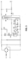
- FIG. 2 is a schematic illustrating another power supply embodiment in which primary side control is provided to regulate the output voltage 211 in a flyback power supply converter.
- the input fuse, rectification and EMI filter is shown as a single block 200 and is similar to block 100 of Figure 1 and can be appreciated to one skilled in the art.
- Components 201, 202, 203 and 204 form a clamp circuit, which limits the peak voltage across regulator 206. As in the embodiment described previously in Figure 1, this clamp is utilized to address the leakage energy stored in the primary of the transformer 212. In the embodiment of Figure 2, this clamp circuit is also used to provide feedback to regulator 206.
- the voltage across capacitor 204 is related to the output voltage 211 through the turns ratio of the transformer main input winding 207 and output winding 208.
- the main transformer winding 207 also acts as the sense winding to provide information regarding the converter output voltage across output winding 208.
- Regulator 206 which can for example be a LinkSwitch from Power Integrations of San Jose, CA, controls the voltage across capacitor 204 by responding to feedback current in resistor 203.
- leakage inductance energy introduces the most significant error in the relationship between the voltages across windings 208 and 207 and again this error degrades output voltage regulation as the power converter output load conditions vary.
- resistor 201 is included to form a low pass filter with capacitor 204 to partially filter the leakage inductance voltage spike appearing across transformer winding 207.
- the improvement in output voltage regulation that this resistor provides may not always be adequate for the load connected to the converter output.
- the resistor-capacitor (RC) time constant of resistor 311 and capacitor 310 is designed such that the discharge of capacitor 310 is much faster than that of capacitor 308, which in the illustrated embodiment discharges through the feedback zener diode 307 into regulator 305.
- the capacitor 310 has a substantially lower voltage than capacitor 308 at the start of the regulator 305 internal switch off time when the leakage inductance spike appears across sense winding 314. The leakage inductance energy therefore charges capacitor 310 substantially without influencing the voltage across capacitor 308.
- the voltage across sense winding 314 is related to the voltage across output winding 316 by the turns ratio between these windings. Capacitors 310 and 308 are therefore charged to this voltage during the conduction time of output diode 317. In this way, the voltage across capacitor 308 is a more accurate representation of the power supply output voltage 319.
- diode 309 is coupled to prevent capacitor 308 from being discharged through resistor 311.
- resistor 313 is coupled to sense winding 314 and forms a low pass filter with capacitor 310 to further filter the leakage inductance voltage spike. The improvement in output regulation provided by the embodiment described above, however, may allow the inclusion of resistor 313 to be optional in accordance with the teachings of the present invention.
- regulator 405 regulates the voltage across capacitor 407 by responding to a feedback current flowing through resistor 404.
- the RC time constant of capacitor 408 and resistor 409 is designed to be much shorter than the time constant of resistor 404 and capacitor 407. In this way, the capacitor 408 has a substantially lower voltage than capacitor 407 at the start of the regulator 405 internal switch off time when the leakage inductance spike appears across sense winding 410. The leakage inductance energy from transformer 415 therefore charges capacitor 408 substantially without influencing the voltage across capacitor 407.
- Figure 5 shows another embodiment of a power supply in which improved converter output voltage regulation is provided in accordance with the teachings of the present invention.
- the embodiment illustrated in Figure 5 shares similarities with the embodiment shown in Figure 3.
- the control signal received by the regulator circuit 505 is a voltage signal and the voltage across capacitor 507 is therefore applied directly to the control pin of regulator 505.
- resistor 506 is coupled to capacitor 507 is provides a discharge path for 507 to ensure that peak charging of capacitor 507 does not corrupt the relationship between the voltage across capacitor 507 and the voltage across the transformer output winding 515.
- resistor 506 is chosen such that the RC time constant of capacitor 507 and resistor 506 is longer than the time constant of resistor 510 and capacitor 509.
- resistor 506 could be eliminated altogether since the input impedance of the control pin of regulator 505 is finite and therefore will discharge capacitor 507 at a rate dependent on the input impedance of the control pin of regulator 505.
- the RC time constant of resistor 510 and capacitor 509 is chosen to be shorter than the time constant set up by the capacitor 507 and the input impedance of the control of regulator 505.
- the voltage control signal received by the regulator circuit 505 could be derived from the voltage across capacitor 507 using a resistor divider connected across capacitor 507 instead of a direct connection between the regulator circuit 505 and capacitor 507 as shown.
Landscapes
- Engineering & Computer Science (AREA)
- Power Engineering (AREA)
- Dc-Dc Converters (AREA)
Priority Applications (1)
| Application Number | Priority Date | Filing Date | Title |
|---|---|---|---|
| EP07023936A EP1912322A1 (de) | 2002-11-05 | 2003-03-12 | Verfahren und Vorrichtung zur Ausgangsspannungsregulierung in primär gesteuerten Schaltmodus-Netzteilen |
Applications Claiming Priority (2)
| Application Number | Priority Date | Filing Date | Title |
|---|---|---|---|
| US287891 | 2002-11-05 | ||
| US10/287,891 US6775155B2 (en) | 2002-11-05 | 2002-11-05 | Method and apparatus for output voltage regulation in primary controlled switched mode power supplies |
Related Child Applications (1)
| Application Number | Title | Priority Date | Filing Date |
|---|---|---|---|
| EP07023936A Division EP1912322A1 (de) | 2002-11-05 | 2003-03-12 | Verfahren und Vorrichtung zur Ausgangsspannungsregulierung in primär gesteuerten Schaltmodus-Netzteilen |
Publications (2)
| Publication Number | Publication Date |
|---|---|
| EP1418662A2 true EP1418662A2 (de) | 2004-05-12 |
| EP1418662A3 EP1418662A3 (de) | 2005-02-09 |
Family
ID=32107621
Family Applications (2)
| Application Number | Title | Priority Date | Filing Date |
|---|---|---|---|
| EP07023936A Withdrawn EP1912322A1 (de) | 2002-11-05 | 2003-03-12 | Verfahren und Vorrichtung zur Ausgangsspannungsregulierung in primär gesteuerten Schaltmodus-Netzteilen |
| EP03251497A Withdrawn EP1418662A3 (de) | 2002-11-05 | 2003-03-12 | Verfahren und Vorrichtung zur Ausgangsspannungsregelung für primärgesteuerte Schaltnetzteile |
Family Applications Before (1)
| Application Number | Title | Priority Date | Filing Date |
|---|---|---|---|
| EP07023936A Withdrawn EP1912322A1 (de) | 2002-11-05 | 2003-03-12 | Verfahren und Vorrichtung zur Ausgangsspannungsregulierung in primär gesteuerten Schaltmodus-Netzteilen |
Country Status (3)
| Country | Link |
|---|---|
| US (5) | US6775155B2 (de) |
| EP (2) | EP1912322A1 (de) |
| JP (1) | JP4084684B2 (de) |
Cited By (3)
| Publication number | Priority date | Publication date | Assignee | Title |
|---|---|---|---|---|
| US7515440B2 (en) | 2002-11-05 | 2009-04-07 | Power Integrations, Inc. | Method and apparatus for output voltage regulation in primary control switched mode power supplies |
| EP2523323A1 (de) * | 2011-05-11 | 2012-11-14 | Siemens Aktiengesellschaft | Frequenzumrichter mit Gleichtaktdrossel und Verfahren zum Betreiben desselben |
| EP2523331A1 (de) * | 2011-05-11 | 2012-11-14 | Siemens Aktiengesellschaft | Frequenzumrichter mit Erdschlussschutz und Verfahren zum Betreiben desselben |
Families Citing this family (29)
| Publication number | Priority date | Publication date | Assignee | Title |
|---|---|---|---|---|
| JPH0569277U (ja) * | 1992-02-24 | 1993-09-21 | 新日軽株式会社 | ドア取付け用蝶板 |
| CN101156305B (zh) * | 2005-04-08 | 2010-05-26 | 奥地利西门子公司 | 用于运行具有初级端泄漏能量反馈的开关电源部件的方法 |
| WO2006138713A1 (en) * | 2005-06-16 | 2006-12-28 | Agere Systems Inc. | Transformerless power over ethernet system |
| US7685440B2 (en) * | 2005-07-21 | 2010-03-23 | Agere Systems Inc. | Switch with fully isolated power sourcing equipment control |
| GB2438463A (en) | 2006-05-23 | 2007-11-28 | Cambridge Semiconductor Ltd | Regulating the output of a switch mode power supply |
| WO2007135453A2 (en) * | 2006-05-23 | 2007-11-29 | Cambridge Semiconductor Limited | Switch mode power supply controllers |
| WO2007135452A1 (en) * | 2006-05-23 | 2007-11-29 | Cambridge Semiconductor Limited | Switch mode power supply controllers |
| US8446746B2 (en) * | 2006-05-23 | 2013-05-21 | Cambridge Semiconductor Limited | Switch mode power supply controller with feedback signal decay sensing |
| US7248487B1 (en) | 2006-06-01 | 2007-07-24 | Cambridge Semiconductor Limited | Switch mode power supply controllers |
| GB2438464A (en) * | 2006-05-23 | 2007-11-28 | Cambridge Semiconductor Ltd | Regulating the output of a switch mode power supply |
| GB2438465B (en) * | 2006-05-23 | 2008-05-21 | Cambridge Semiconductor Ltd | Switch mode power supply controllers |
| GB2439998A (en) * | 2006-07-07 | 2008-01-16 | Cambridge Semiconductor Ltd | Estimating the output current of a switch mode power supply |
| GB2439997A (en) * | 2006-07-07 | 2008-01-16 | Cambridge Semiconductor Ltd | Estimating the output current of a switch mode power supply |
| US7471531B2 (en) | 2006-08-22 | 2008-12-30 | Agere Systems Inc. | Programmable feedback voltage pulse sampling for switched power supplies |
| US7843670B2 (en) * | 2006-09-29 | 2010-11-30 | Agere Systems Inc. | Isolated switched maintain power signature (MPS) and fault monitoring for power over Ethernet |
| US7996166B2 (en) * | 2007-03-26 | 2011-08-09 | Agere Systems Inc. | Isolated capacitive signature detection for powered devices |
| US7643320B2 (en) | 2007-03-28 | 2010-01-05 | Agere Systems Inc. | Isolated resistive signature detection for powered devices |
| JP5121307B2 (ja) * | 2007-05-28 | 2013-01-16 | ソニーモバイルコミュニケーションズ株式会社 | 無接点電力伝送コイルユニット、携帯端末、送電装置、及び、無接点電力伝送システム |
| US7808802B2 (en) * | 2007-09-06 | 2010-10-05 | Jun Cai | Isolated switched-mode power supply with output regulation from primary side |
| US7916505B2 (en) * | 2008-03-06 | 2011-03-29 | Enphase Energy, Inc. | Method and apparatus for a leakage energy recovery circuit |
| US8923015B2 (en) | 2008-11-26 | 2014-12-30 | Auckland Uniservices Limited | Primary-side power control for inductive power transfer |
| EP2209199A1 (de) * | 2009-01-20 | 2010-07-21 | ABB Schweiz AG | Verfahren zum Betrieb einer Umrichterschaltung sowie Vorrichtung zur Durchführung des Verfahrens |
| US8213187B2 (en) * | 2009-10-14 | 2012-07-03 | Power Integrations, Inc. | Method and apparatus for high-side input winding regulation |
| US8213192B2 (en) * | 2009-12-30 | 2012-07-03 | Silicon Laboratories Inc. | Primary side sensing for isolated fly-back converters |
| JP6297963B2 (ja) * | 2014-11-05 | 2018-03-20 | 住友電気工業株式会社 | 変圧装置 |
| CN106059302A (zh) * | 2016-07-18 | 2016-10-26 | 宁波三星医疗电气股份有限公司 | 一种开关电源反馈电路 |
| US11418121B2 (en) | 2019-12-30 | 2022-08-16 | Power Integrations, Inc | Auxiliary converter to provide operating power for a controller |
| US11258369B2 (en) | 2020-02-19 | 2022-02-22 | Power Integrations, Inc. | Inductive charging circuit to provide operative power for a controller |
| US12592639B2 (en) | 2023-12-21 | 2026-03-31 | Power Integrations, Inc. | Self-biasing the input controller in a power converter |
Family Cites Families (14)
| Publication number | Priority date | Publication date | Assignee | Title |
|---|---|---|---|---|
| US93839A (en) * | 1869-08-17 | Improvement in glass-house pots | ||
| DE1098094B (de) * | 1959-09-26 | 1961-01-26 | Deutsche Elektronik Gmbh | Einrichtung zur Messung der Spitzenspannung einmaliger kurzzeitiger Spannungsspitzen |
| DE2160259A1 (de) * | 1971-12-04 | 1973-06-07 | Ulrich Knick Elektronische Mes | Aussteuerungsmesser fuer tonfrequenzspannungen mit vermindertem einfluss der spannungskurvenform |
| US4833582A (en) * | 1987-03-27 | 1989-05-23 | Siemens Aktiengesellschaft | Frequency converter circuit including a single-ended blocking frequency converter |
| US5138543A (en) * | 1991-05-31 | 1992-08-11 | At&T Bell Laboratories | Output voltage estimating circuit for a power converter having galvanic isolation between input and output circuits |
| US5345164A (en) * | 1993-04-27 | 1994-09-06 | Metcal, Inc. | Power factor corrected DC power supply |
| DE29515883U1 (de) * | 1995-10-10 | 1995-11-16 | Metz-Werke GmbH & Co KG, 90763 Fürth | Schaltungsanordnung für ein Schaltnetzteil |
| US5661643A (en) * | 1996-02-20 | 1997-08-26 | Eaton Corporation | Universal power module |
| JP3236587B2 (ja) | 1999-09-30 | 2001-12-10 | 長野日本無線株式会社 | スイッチング電源装置 |
| KR100419393B1 (ko) * | 1999-12-09 | 2004-02-21 | 산켄덴키 가부시키가이샤 | Dc-dc 컨버터 |
| US6233161B1 (en) | 2000-03-02 | 2001-05-15 | Power Integrations, Inc. | Switched mode power supply responsive to voltage across energy transfer element |
| JP3985461B2 (ja) | 2000-05-02 | 2007-10-03 | 日本ビクター株式会社 | 認証方法、コンテンツ送信側機器、コンテンツ受信側機器、認証システム |
| FR2816128B1 (fr) | 2000-10-31 | 2003-02-07 | St Microelectronics Sa | Alimentation a decoupage basse tension isolee |
| US6775155B2 (en) * | 2002-11-05 | 2004-08-10 | Power Integrations, Inc. | Method and apparatus for output voltage regulation in primary controlled switched mode power supplies |
-
2002
- 2002-11-05 US US10/287,891 patent/US6775155B2/en not_active Expired - Fee Related
-
2003
- 2003-03-12 EP EP07023936A patent/EP1912322A1/de not_active Withdrawn
- 2003-03-12 EP EP03251497A patent/EP1418662A3/de not_active Withdrawn
- 2003-03-19 JP JP2003074921A patent/JP4084684B2/ja not_active Expired - Fee Related
-
2004
- 2004-07-01 US US10/882,376 patent/US6985368B2/en not_active Expired - Fee Related
-
2005
- 2005-04-05 US US11/100,229 patent/US7027312B2/en not_active Expired - Lifetime
-
2006
- 2006-01-30 US US11/343,559 patent/US7142437B2/en not_active Expired - Fee Related
- 2006-10-17 US US11/582,612 patent/US7515440B2/en not_active Expired - Fee Related
Cited By (3)
| Publication number | Priority date | Publication date | Assignee | Title |
|---|---|---|---|---|
| US7515440B2 (en) | 2002-11-05 | 2009-04-07 | Power Integrations, Inc. | Method and apparatus for output voltage regulation in primary control switched mode power supplies |
| EP2523323A1 (de) * | 2011-05-11 | 2012-11-14 | Siemens Aktiengesellschaft | Frequenzumrichter mit Gleichtaktdrossel und Verfahren zum Betreiben desselben |
| EP2523331A1 (de) * | 2011-05-11 | 2012-11-14 | Siemens Aktiengesellschaft | Frequenzumrichter mit Erdschlussschutz und Verfahren zum Betreiben desselben |
Also Published As
| Publication number | Publication date |
|---|---|
| US7515440B2 (en) | 2009-04-07 |
| JP4084684B2 (ja) | 2008-04-30 |
| US6775155B2 (en) | 2004-08-10 |
| US6985368B2 (en) | 2006-01-10 |
| US20040085782A1 (en) | 2004-05-06 |
| EP1912322A1 (de) | 2008-04-16 |
| JP2004159489A (ja) | 2004-06-03 |
| EP1418662A3 (de) | 2005-02-09 |
| US20060126366A1 (en) | 2006-06-15 |
| US7142437B2 (en) | 2006-11-28 |
| US20070035970A1 (en) | 2007-02-15 |
| US20040246747A1 (en) | 2004-12-09 |
| US20050195623A1 (en) | 2005-09-08 |
| US7027312B2 (en) | 2006-04-11 |
Similar Documents
| Publication | Publication Date | Title |
|---|---|---|
| US6775155B2 (en) | Method and apparatus for output voltage regulation in primary controlled switched mode power supplies | |
| US9293996B2 (en) | Method and apparatus for integrated cable drop compensation of a power converter | |
| US7215105B2 (en) | Method and apparatus for maintaining a constant load current with line voltage in a switch mode power supply | |
| US6643158B2 (en) | Dual input AC/DC to programmable DC output converter | |
| US7339359B2 (en) | Terminal for multiple functions in a power supply | |
| US5959851A (en) | Switched-mode power supply control circuit | |
| US20070035285A1 (en) | Methods and apparatus for maintaining an approximate constant current output characteristic in a switched mode power supply | |
| JP2013226047A (ja) | エネルギ伝達エレメントの入力にわたる電圧から導かれた電流に応答するための回路および方法 | |
| US6016260A (en) | Switched-mode power supply with current and voltage limitation | |
| KR20020079861A (ko) | 2차 펄스폭 변조 제어를 가지는 플라이백 컨버터를 위한시동 회로 | |
| US4595977A (en) | Switched mode power supply | |
| US4325111A (en) | Switched mode regulated DC to DC converter | |
| KR20000001821U (ko) | 순간 입력전압 강하 보상회로 |
Legal Events
| Date | Code | Title | Description |
|---|---|---|---|
| PUAI | Public reference made under article 153(3) epc to a published international application that has entered the european phase |
Free format text: ORIGINAL CODE: 0009012 |
|
| AK | Designated contracting states |
Kind code of ref document: A2 Designated state(s): AT BE BG CH CY CZ DE DK EE ES FI FR GB GR HU IE IT LI LU MC NL PT RO SE SI SK TR |
|
| AX | Request for extension of the european patent |
Extension state: AL LT LV MK |
|
| 17P | Request for examination filed |
Effective date: 20041001 |
|
| PUAL | Search report despatched |
Free format text: ORIGINAL CODE: 0009013 |
|
| AK | Designated contracting states |
Kind code of ref document: A3 Designated state(s): AT BE BG CH CY CZ DE DK EE ES FI FR GB GR HU IE IT LI LU MC NL PT RO SE SI SK TR |
|
| AX | Request for extension of the european patent |
Extension state: AL LT LV MK |
|
| AKX | Designation fees paid |
Designated state(s): DE FR GB IT NL SE |
|
| 17Q | First examination report despatched |
Effective date: 20050928 |
|
| RAP3 | Party data changed (applicant data changed or rights of an application transferred) |
Owner name: POWER INTEGRATIONS, INC. |
|
| STAA | Information on the status of an ep patent application or granted ep patent |
Free format text: STATUS: THE APPLICATION IS DEEMED TO BE WITHDRAWN |
|
| 18D | Application deemed to be withdrawn |
Effective date: 20150414 |