EP1420332B1 - Leistungssteuersystem - Google Patents
Leistungssteuersystem Download PDFInfo
- Publication number
- EP1420332B1 EP1420332B1 EP20030078573 EP03078573A EP1420332B1 EP 1420332 B1 EP1420332 B1 EP 1420332B1 EP 20030078573 EP20030078573 EP 20030078573 EP 03078573 A EP03078573 A EP 03078573A EP 1420332 B1 EP1420332 B1 EP 1420332B1
- Authority
- EP
- European Patent Office
- Prior art keywords
- power
- transformer
- controller
- diode
- saving
- Prior art date
- Legal status (The legal status is an assumption and is not a legal conclusion. Google has not performed a legal analysis and makes no representation as to the accuracy of the status listed.)
- Expired - Lifetime
Links
Images



Classifications
-
- G—PHYSICS
- G06—COMPUTING OR CALCULATING; COUNTING
- G06F—ELECTRIC DIGITAL DATA PROCESSING
- G06F1/00—Details not covered by groups G06F3/00 - G06F13/00 and G06F21/00
- G06F1/26—Power supply means, e.g. regulation thereof
- G06F1/32—Means for saving power
- G06F1/3203—Power management, i.e. event-based initiation of a power-saving mode
- G06F1/3206—Monitoring of events, devices or parameters that trigger a change in power modality
- G06F1/3215—Monitoring of peripheral devices
- G06F1/3218—Monitoring of peripheral devices of display devices
-
- G—PHYSICS
- G06—COMPUTING OR CALCULATING; COUNTING
- G06F—ELECTRIC DIGITAL DATA PROCESSING
- G06F1/00—Details not covered by groups G06F3/00 - G06F13/00 and G06F21/00
- G06F1/26—Power supply means, e.g. regulation thereof
-
- G—PHYSICS
- G06—COMPUTING OR CALCULATING; COUNTING
- G06F—ELECTRIC DIGITAL DATA PROCESSING
- G06F1/00—Details not covered by groups G06F3/00 - G06F13/00 and G06F21/00
- G06F1/26—Power supply means, e.g. regulation thereof
- G06F1/32—Means for saving power
- G06F1/3203—Power management, i.e. event-based initiation of a power-saving mode
- G06F1/3234—Power saving characterised by the action undertaken
- G06F1/325—Power saving in peripheral device
- G06F1/3265—Power saving in display device
-
- G—PHYSICS
- G09—EDUCATION; CRYPTOGRAPHY; DISPLAY; ADVERTISING; SEALS
- G09G—ARRANGEMENTS OR CIRCUITS FOR CONTROL OF INDICATING DEVICES USING STATIC MEANS TO PRESENT VARIABLE INFORMATION
- G09G1/00—Control arrangements or circuits, of interest only in connection with cathode-ray tube indicators; General aspects or details, e.g. selection emphasis on particular characters, dashed line or dotted line generation; Preprocessing of data
- G09G1/005—Power supply circuits
-
- H—ELECTRICITY
- H02—GENERATION; CONVERSION OR DISTRIBUTION OF ELECTRIC POWER
- H02J—ELECTRIC POWER NETWORKS; CIRCUIT ARRANGEMENTS OR SYSTEMS FOR SUPPLYING OR DISTRIBUTING ELECTRIC POWER; SYSTEMS FOR STORING ELECTRIC ENERGY
- H02J9/00—Circuit arrangements for emergency or stand-by power supply, e.g. for emergency lighting
- H02J9/005—Circuit arrangements for emergency or stand-by power supply, e.g. for emergency lighting using a power saving mode
-
- G—PHYSICS
- G09—EDUCATION; CRYPTOGRAPHY; DISPLAY; ADVERTISING; SEALS
- G09G—ARRANGEMENTS OR CIRCUITS FOR CONTROL OF INDICATING DEVICES USING STATIC MEANS TO PRESENT VARIABLE INFORMATION
- G09G2330/00—Aspects of power supply; Aspects of display protection and defect management
- G09G2330/02—Details of power systems and of start or stop of display operation
- G09G2330/021—Power management, e.g. power saving
- G09G2330/022—Power management, e.g. power saving in absence of operation, e.g. no data being entered during a predetermined time
-
- H—ELECTRICITY
- H04—ELECTRIC COMMUNICATION TECHNIQUE
- H04N—PICTORIAL COMMUNICATION, e.g. TELEVISION
- H04N5/00—Details of television systems
- H04N5/63—Generation or supply of power specially adapted for television receivers
-
- Y—GENERAL TAGGING OF NEW TECHNOLOGICAL DEVELOPMENTS; GENERAL TAGGING OF CROSS-SECTIONAL TECHNOLOGIES SPANNING OVER SEVERAL SECTIONS OF THE IPC; TECHNICAL SUBJECTS COVERED BY FORMER USPC CROSS-REFERENCE ART COLLECTIONS [XRACs] AND DIGESTS
- Y02—TECHNOLOGIES OR APPLICATIONS FOR MITIGATION OR ADAPTATION AGAINST CLIMATE CHANGE
- Y02D—CLIMATE CHANGE MITIGATION TECHNOLOGIES IN INFORMATION AND COMMUNICATION TECHNOLOGIES [ICT], I.E. INFORMATION AND COMMUNICATION TECHNOLOGIES AIMING AT THE REDUCTION OF THEIR OWN ENERGY USE
- Y02D10/00—Energy efficient computing, e.g. low power processors, power management or thermal management
-
- Y—GENERAL TAGGING OF NEW TECHNOLOGICAL DEVELOPMENTS; GENERAL TAGGING OF CROSS-SECTIONAL TECHNOLOGIES SPANNING OVER SEVERAL SECTIONS OF THE IPC; TECHNICAL SUBJECTS COVERED BY FORMER USPC CROSS-REFERENCE ART COLLECTIONS [XRACs] AND DIGESTS
- Y02—TECHNOLOGIES OR APPLICATIONS FOR MITIGATION OR ADAPTATION AGAINST CLIMATE CHANGE
- Y02D—CLIMATE CHANGE MITIGATION TECHNOLOGIES IN INFORMATION AND COMMUNICATION TECHNOLOGIES [ICT], I.E. INFORMATION AND COMMUNICATION TECHNOLOGIES AIMING AT THE REDUCTION OF THEIR OWN ENERGY USE
- Y02D30/00—Reducing energy consumption in communication networks
- Y02D30/50—Reducing energy consumption in communication networks in wire-line communication networks, e.g. low power modes or reduced link rate
Definitions
- the present invention relates to a power controlling system of a display monitor, more particularly, to a power controlling system of a computer monitor and a method thereof, capable of minimizing power consumption for automatically converting a monitor power mode to a power off mode in case that the computer is not used for a certain period of time.
- a power supply circuit in the computer monitor automatically switches a power mode of the computer to a power saving mode until a user presses any key on a keyboard, thereby saving unnecessary power consumption.
- Recent monitors in the current market mostly have this function.
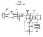
- Fig. 1 is a circuit diagram of a related art power supply circuit of a monitor. The discussion on the related art power supply circuit follows below.
- the power supply circuit includes a power input 100 for decompressing input power (AC), a noise filter 110 for filtering noises using output voltage of the power input 100 when a power switch SW1 is turned on, a rectifier 120 for rectifying the output voltage of the noise filter 100 at a bridge diode (BD1) and a condenser C1 and for dividing the rectified voltage Vd through resistors R1 to R3, a power switch 140 for outputting a switching signal by means of voltage division of the rectifier 120, and a voltage output 130 for outputting DC voltage by inducing an output of the rectifier to a secondary side transformer T1 according to an output of the power switch 140.
- AC decompressing input power
- BD1 bridge diode
- C1 condenser
- the problem of the above power supply circuit is that unless the user turns off the power of the monitor, power is continuously supplied to the monitor even when the user is not currently using the computer. As a result, element lifespans in the circuit are dramatically shortened, and thus the reliability of the power supply circuit is lowered.
- Korean patent application No. 10-1998-0048370 disclosed an embodiment of a power-saving circuit.
- Fig. 2 is a circuit diagram of a power-saving circuit disclosed in the above patent application.
- the power-saving circuit includes a rectifier 200 for rectifying and smoothing AC power, a power factor controller 210 for outputting the AC power as power factor-compensated DC voltage, power controllers 220 and 240 for controlling a plurality of transformers, having them output a plurality of different voltages from the applied DC voltage, a microcomputer 270 (Micom) used as a controller for controlling the overall power circuit and for outputting a plurality of DPM (Display Power Management) control signals in DPM mode, power-saving parts 250 and 260 for outputting a heater power or light emitting signal in response to the DPM control signal, and a main power switch 230 for supplying or switching off power voltage Vcc applied to the power controller 220 under the light emitting signal.
- a microcomputer 270 Microcomputer 270
- DPM Display Power Management
- Display Power Management control signals in DPM mode, power-saving parts 250 an d 260 for outputting a heater power or light emitting signal in response to the DPM co ntrol signal, and a main power switch 230 for supplying or switching off power voltage Vcc applied to the power controller 220 under the light emitting signal.
- the power-saving circuit satisfies the 2000 IECC, i.e. its power is set at 3 Watt in the power off mode.
- this type of power-saving circuit does not satisfy the European regulations, Blue Angel, requiring the power consumption in the power off mode to b e less than 1 Watt.
- the sub power controller 240, the M icom power (+B7), and the heater power (+B8) continue their operation by an output of the rectifier, by the sub power, and by the first power-saving part, respectively.
- GB2343823 discloses a power saving part connected to the secondary side of a sub transformer, but does not disclose two power-saving parts that are connected to an arbitrary point of the secondary side of a main transformer and output predetermined voltages in response to control signals (DPMF, DPMS) which are output from a controller.
- DPMF control signals
- US5870086 discloses a power-saving part (21, Q11) connected to the primary side of a main transformer, but does not disclose two power-saving parts that are connected to an arbitrary point of the secondary side of a main transformer and output predetermined voltages in response to control signals (DPMF, DPMS) which are output from a controller.
- DPMF control signals
- US61848751 discloses a power saving part (25, 23, 24) connected to the secondary side of a sub transformer, but does not disclose two power-saving parts that are connected to an arbitrary point of the secondary side of a main transformer and output predetermined voltages in response to control signals (DPMF, DPMS) which are output from a controller.
- DPMF control signals
- An object of the invention is to solve at least the above problems and/or disadvantages and to provide at least the advantages described hereinafter.
- one object of the present invention is to solve the above problems by providing a power controlling system for a computer, whose power consumption in a power off mode is less than 1 Watt.
- the objectives are achieved by a display monitor power controlling system according to claim 1 and a power controlling method according to claim 43.
- a power controlling system including: a power supply means for rectifying and/or co elements except the controller according to the DPM mode; and a transformer controller for outputting power to control the transformers under the control of the power control means.
- a power controlling system having a main transformer and a sub transformer, which, in response to first and second DPM signals output from a display controller, from an AC voltage being input from outside, induces at least one voltage, for use in a display, from secondary sides of the main transformer and the sub transformer, and outputs the induced voltages
- the system includes: a first power-saving part connected to an arbitrary point of a secondary side of the main transformer, for outputting a predetermined voltage in response to the first DPM signal output from the controller; a second power-saving part connected to an arbitrary point of a secondary side of the main transformer, for outputting a predetermined voltage in response to the second DPM signal output from the controller; a third power-saving part connected to the first and second power-saving parts, which turns off as the first power-saving part is turned off; a main power switch connected to one end of a primary side of the main transformer, for controlling an operation of the main transformer; and a transformer controller for controlling an operation of the main power switch according to an
- Another aspect of the invention provides a power controlling method, which includes the steps of: determining an input DPM mode to a power-saving part used as a power control means; controlling an output of the power-saving part according to the input signals, when input DPM signals are all low level signals; controlling at least one of the power-saving part, another power-saving part, and a transformer controller used as a main power controller, under an operation of the power-saving part or an output thereof; and operating a sub power to supply power only to the controller, after controlling the main power controller.
- a power off mode in a power off mode, only the Micom is being turned on and the rest of elements are all turned off.
- Power consumption of a display in the power off mode is less than 1 Watt, which satisfies the European regulations, Blue Angel.
- the operation of the Micom is more stabilized.
- Fig. 1 is a schematic block diagram illustrating a power supply circuit for a monitor according to a related art
- Fig. 2 is a schematic block diagram illustrating a power supply circuit with a power saving function according to a related art
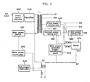
- Fig. 3 is a schematic block diagram illustrating a power supply circuit for a monitor according to a preferred embodiment of the present invention
- Fig. 4 is a detailed view of Fig. 3 ;
- Fig. 5 is a diagram illustrating first and second DPM signals according to respective DPM (Display Power Management) modes of the Micom;
- Fig. 6 is an operational flow chart of a power supply circuit according to the present invention.
- Fig. 7 is an operational flow chart of a power supply circuit of the present invention when DPM mode is low.
- Figs. 3 through 7 show the organization and the operation of the power supply circuit for a monitor.
- +B1 denotes horizontal deflection DC/DC Converter input power
- +B2 denotes video output circuit power
- +B3 denotes horizontal/vertical power
- +B4 denotes other circuit power
- +B5 denotes vertical IC driving power
- +B6 denotes heater power.
- Fig. 3 is a schematic block diagram illustrating a power supply circuit for a monitor according to a preferred embodiment of the present invention
- Fig. 4 is a detailed view of Fig. 3 .
- the power controlling system includes a main transformer T1, a sub transformer T2, a power factor controller 300, a rectifier 310, a main power switch 330, a main power controller consisting of a light-transmitting part 322 and a light-receiving part 320, a sub power controller 340, a first power-saving part 350, a second power-saving part 360, a third power-saving part 380, and a microcomputer 370 (Micom) that is used as a controller.
- a microcomputer 370 Micom
- the power factor controller 300 and the rectifier 310 are connected between an input power and a primary side of the main transformer T1, compensating power factor of the AC power that is input from outside, rectifying and smoothing the AC power, and finally supplying the DC voltage to the main transformer T1.
- the primary sides of the main transformer T1 and the sub transformer T2 receive DC voltage from the rectifier 310, and output to the secondary sides different voltages to be used for each circuit in the monitor.
- One end of the primary side of the main transformer T1 is connected to the rectifier 310 and the other end is connected to the main power switch 330.
- one end of the primary side of the sub transformer T2 is connected to the rectifier 310 and the other end is connected to the sub power controller 340.
- the first power-saving part 350 is connected to an arbitrary position of the secondary side of the main transformer T1, and in DPM mode, outputs a designated voltage (+B3) in response to a DPMF (Display Power Management First) signal from the Micom 370.
- DPMF Display Power Management First
- the first power-saving part 350 includes transistors Q1 and Q2, and resistors R1, R2 and R3.
- the emitter of the transistor Q1 is connected to an arbitrary position of the secondary side of the main transformer T1 via a diode D1, the collector of the transistor, which is an output terminal, outputs the +B3 voltage, and the base is connected to the collector of the transistor Q2 through the resistor R2.
- the base of the transistor Q2 is where a first DPM signal (DPMF signal) of the Micom is input via the resistor R3.
- the emitter of the transistor Q2 is put to earth.
- the resistor R1 is inserted between the emitter and the base of the transistor Q1.
- the transistor Q1 and Q2 is a PNP transistor and an NPN transistor, respectively.
- the second power-saving part 360 is connected to an arbitrary position of the secondary side of the main transformer T1, and in DPM mode, outputs a designated voltage (+B4) in response to a second DPM signal (DPMS signal) from the Micom 370.
- DPMS signal second DPM signal
- the second power-saving part 360 includes transistors Q3 and Q5, a diode D5, and resistors R4 and R5.
- the transistors Q3 and Q5 are preferably a PNP transistor and an NPN transistor, respectively.
- the emitter of the transistor Q3 is connected to an arbitrary point of the secondary side of the main transformer T1 via a diode D2, the base of the transistor Q3 is connected to the collector of the transistor Q5 via the resistor R5, and the collector of the transistor Q3, which is an output terminal, outputs the +B4 voltage.
- the base of the transistor Q5 is where a DPMS signal from the Micom is input, the collector of the transistor Q5 is connected to the base of the transistor Q1 via the resistor R5, and the emitter of the transistor Q5 is earthed.
- the resistor R4 is inserted between the emitter and the base of the transistor Q3.
- the cathode of the diode D5 is connected to the emitter of the transistor Q3, and the anode of the diode D5 is connected to the secondary side of the sub transformer T2 via the diode D6.
- the third power-saving part 380 is connected to the output end of the first and second power-saving parts 350 and 360, and outputs a designated voltage (+B6).
- the third power-saving part 380 includes a transistor Q4, a Zener diode ZD1, and a diode D3.
- the transistor Q4 is preferably an NPN transistor.
- the base of the transistor Q4 is connected to the collector of the transistor Q1 of the first power-saving part 350 via a resistor R9, the collector of the transistor Q4 of the third power-saving part 380 is connected to the collector of the transistor Q3 of the second power-saving part 360, and the emitter of the transistor Q4 of the third power-saving part 380, which is an output terminal, outputs the +B6 voltage.
- the anode of the Zener diode ZD1 is connected to the anode of the diode D3, and the cathode of the Zener diode ZD1 is connected to the base of the transistor Q4.
- the anode of the diode D3 is connected to the anode of the Zener diode ZD1, and the cathode of the diode D3 is earthed.
- the main power controller includes the light-transmitting part 322 and the light-receiving part 320.
- the light-transmitting part 322 is connected to one end of the second power-saving part and to the secondary side of the sub transformer T2.
- the light-receiving part 320 is connected to the main power switch 330 and to the tertiary side of the sub transformer T2.
- the light-transmitting part 322 includes a diode D4 and a photo diode PD1
- the light-receiving part 320 includes a diode D7, a resistor R7, and a phototransistor PT1.
- the photo diode PD1 of the light-transmitting part and the phototransistor PT1 of the light-receiving part are used as a light-emitting element and a light-receiving element, respectively.
- the cathode of the diode D4 is connected to the base of the transistor Q3 of the second power-saving part, and the anode of the diode D4 is connected to the cathode of the photo diode PD1.
- the anode of the photo diode PD1 is connected to the secondary side of the sub transformer T2 via the diode D6.
- the phototransistor PT1, together with the photo diode PD1, composes a photo coupler.
- the emitter of the phototransistor PT1 is connected to Vcc of the main power switch 330, and the collector of the phototransistor PT1 is connected to the cathode of the diode D7 via the resistor R7.
- the anode of the diode D7 is connected to one end of the tertiary side sub transformer T2.
- the main power switch 330 is turned on or off, being controlled by an output signal from the light-receiving part 320 of the main power controller.
- the input voltage Vcc to the main power switch 330 is connected to the emitter of the phototransistor PT1 of the light-receiving part 320.
- the power controlling system controls the first and second power-saving parts according to the first DPM signal (DPMF signal) and the second DPM signal (DPMS signal) from the Micom, and using at least one output of the first and second power-saving parts, controls the third power-saving part and/or the main power controller.
- the power factor controller 300 compensates the power factor of the AC voltage and applies the AC voltage to the rectifier 310.
- the rectifier 310 converts the AC voltage to a DC voltage, and supplies the DC voltage to the primary side of the main transformer T1 and the primary side of the sub transformer T2.
- the power supplied to the primary side of the main transformer T1 is controlled by the main power switch 330, that is in turn controlled by the main power controller.
- the power supplied to the primary side of the sub transformer T2 is controlled by the sub power controller 340.
- Fig. 5 is a diagram illustrating a first and a second DPM signal in DPM mode. As shown in Fig. 5 , in normal mode, the DPMF signal is high and the DPMS signal is also high.
- the DPMF signal is low and the DPMS signal is high.
- the DPMF signal output from the Micom is a high level signal.
- the transistor Q2 of the first power-saving part 350 is turned on, and the +B3 voltage is supplied. Accordingly, the voltage is fed to the base of the transistor Q4 of the third power-saving part 380, so the transistor Q4 is turned on and the +B6 voltage is supplied.
- the transistor Q5 and the transistor Q3 of the second power-saving part 360 are turned on, and as a result thereof, the +B4 and +B6 voltage are output.
- the voltage on the base of the transistor Q3 is lowered, and thus, a current flows in the photo diode PD1 of the light-transmitting part 322, turning on the photo diode PD1. Therefore, the phototransistor PT1 of the light-receiving part 320 is turned on, and as a result thereof, the voltage Vcc is supplied to the main power switch 330.
- the transistors Q5 and Q3 of the second power-saving part 360 are turned on, and as a result thereof, the +B4 voltage is output. Moreover, the voltage on the base of the transistor Q3 is lowered, and thus, a current flows in the photodiode PD1 of the light-transmitting part 322. Therefore, the phototransistor PT1 of the light-receiving part 320 of the main power controller is turned on, and the voltage Vcc is supplied to the main power switch 330. Accordingly, energy is transferred to the secondary side of the main transformer T1, and B1, B2, B4, B5 and B7 voltages are supplied thereby.
- the +B3 and +B6 voltages are not output because the DPMF signal is a low level signal.
- the transistor Q1 of the first power-saving part 350 is turned off and the +B3 voltage is not output.
- the transistor Q4 of the third power-saving part is turned off and the +B6 voltage is not output, either.
- the transistor Q5 of the second power-saving part 360 is turned off.
- the transistor Q3 is turned off and the +B4 voltage is not output.
- the photo coupler Ph1 which is a photo diode for the light-transmitting part 322 and for the light-receiving part 320, is turned off, and thus, Vcc is not supplied to the main power switch 330. Therefore, no voltage can be induced to the secondary side of the main transformer T1, and the +B1, +B2, and +B5 voltages are not output.
- the +B1 through +B6 voltages are off, and the power mode of the monitor becomes the power off mode to which the +B7 voltage only is applied.
- Fig. 6 is an operational flow chart of a power supply circuit according to the present invention.
- DPM mode being input to a power-saving part or power output control means is determined (S601).
- input DPM signals are the DPMF signal and the DPMS signal, and depending on the signal, the DPM mode can be in standby mode or in off mode.
- the power-saving part By the operation or output of the power-saving part, the power-saving part, the other power-saving part, and the main power controller that controls the transformer, are all or respectively controlled (S603).
- a transistor of the power-saving part As a transistor of the power-saving part, to which low DPM signals are applied, is controlled, a base voltage of the corresponding transistor is increased. Then, a main power controller including a light-transmitting part is controlled and only sub power is supplied to a controller (S604).
- Fig. 7 is an operational flow chart of a power supply circuit of the present invention when DPM mode is low.
- At least one DPM signals i.e., DPMF and DPMS signals, are input to a power-saving part as low level signals (S701).
- the power-saving part By the operation or output of the power-saving part, the power-saving part, the other power-saving part, and the main power controller including the light-transmitting and light-receiving parts, are all or respectively controlled (S702).
- a main power switch controls a main transformer (S703), and a sub transformer supplies power only to Micom, i.e., the controller (S704).
- the transistor Q5 when the DPMF/DPMS signals are output in "Low” and “Low” levels, the transistor Q5 is turned off, the base voltage of the transistor Q3 is increased higher than +B6 voltage. This cuts off the current to the PD1 322 so the PT1 320 and the main power switch are turned off.
Landscapes
- Engineering & Computer Science (AREA)
- Theoretical Computer Science (AREA)
- Physics & Mathematics (AREA)
- General Physics & Mathematics (AREA)
- General Engineering & Computer Science (AREA)
- Remote Sensing (AREA)
- Radar, Positioning & Navigation (AREA)
- Computer Hardware Design (AREA)
- Business, Economics & Management (AREA)
- Emergency Management (AREA)
- Power Engineering (AREA)
- Dc-Dc Converters (AREA)
- Control Of Electrical Variables (AREA)
- Direct Current Feeding And Distribution (AREA)
Claims (45)
- System zur Steuerung der Leistung eines Anzeigemonitors mit:einer Stromversorgungseinrichtung (300, 310) zum Gleichrichten und/oder Kompensieren einer Eingangsleistung;einem Haupt- und Nebentransformator (T1, T2) mit jeweils einer Primärseite zum Empfangen der Leistung von der Stromversorgungseinrichtung (300, 310) und Sekundärseiten zum Abgeben von Spannungen zur Verwendung für jede Schaltung in einem Monitor,einer Steuereinrichtung (370) zum Ausgeben mehrerer Anzeigeenergieverwaltungs-, DPM-Steuersignale, wobei die Steuereinrichtung (370) von der Sekundärseite des Nebentransformators versorgt wird,dadurch gekennzeichnet, daß das Leistungssteuersystem ferner aufweist:ein erstes Leistungssparteil (350) und ein zweites Leistungssparteil (360), die mit einem beliebigen Punkt einer Sekundärseite eines Haupttransformators (T1) verbunden sind und vorbestimmte Spannungen abgeben bzw. abschalten, die zur Lieferung von Leistung an Elemente im Monitor als Antwort auf die DPM-Steuersignale zu verwenden sind,ein weiteres gesondertes Leistungssparteil (380), das mit dem ersten (350) und/oder dem zweiten (360) Leistungssparteil verbunden ist und eine vorbestimmte Spannung abgibt; undeine Transformatorsteuereinrichtung (320, 322) zum Abgeben von Leistung zur Steuerung des Haupttransformators (T1) unter der Steuerung mindestens einer der Leistungssparteile (360).
- System nach Anspruch 1, dadurch gekennzeichnet, daß es ferner einen Hauptschalter zur Steuerung der Transformatoren durch ein Ausgangssignal der Transformatorsteuereinrichtung aufweist.
- System nach Anspruch 1, dadurch gekennzeichnet, daß die Stromversorgungseinrichtung eine Leistungsfaktorsteuereinrichtung und einen Gleichrichter aufweist, die zwischen eine Eingangsleistung und eine Primärseite eines Haupttransformators geschaltet sind, zum Zuführen von Ausgangsspannung zum Haupttransformator durch Kompensieren eines Leistungsfaktors und/oder Glätten einer Eingangsleistung von außen.
- System nach Anspruch 1, dadurch gekennzeichnet, daß die Primärseite des Haupttransformators und des Nebentransformators eine Gleichspannung vom Gleichrichter empfängt.
- System nach Anspruch 4, dadurch gekennzeichnet, daß ein Ende der Primärseite des Haupttransformators mit dem Gleichrichter verbunden ist und das andere Ende mit dem Hauptschalter verbunden ist.
- System nach Anspruch 4, dadurch gekennzeichnet, daß ein Ende der Primärseite des Nebentransformators mit dem Gleichrichter verbunden ist und das andere Ende mit der Nebenleistungssteuereinrichtung verbunden ist.
- System nach einem der vorhergehenden Ansprüche, dadurch gekennzeichnet, daß das erste Leistungssparteil mindestens einen Transistor (Q1, Q2) und mindestens einen Widerstand aufweist.
- System nach Anspruch 7, dadurch gekennzeichnet, daß ein Emitter von Q1 mit einem beliebigen Punkt eines Haupttransformators über eine Diode (D1) verbunden ist.
- System nach Anspruch 7, dadurch gekennzeichnet, daß ein Kollektor von Q1 ein Ausgangsanschluß zum Abgeben einer vorbestimmten Spannung ist und eine Basis von Q1 mit einem Kollektor von Q2 über einen Widerstand verbunden ist.
- System nach Anspruch 7, dadurch gekennzeichnet, daß ein DPMF-Signal, das ein erstes DPM-Signal der Steuereinrichtung ist, über einen Widerstand in die Basis von Q2 eingegeben wird.
- System nach Anspruch 7, dadurch gekennzeichnet, daß der Transistor Q1 und Q2 ein PNP-Transistor bzw. ein NPN-Transistor ist.
- System nach einem der vorhergehenden Ansprüche, dadurch gekennzeichnet, daß das zweite Leistungssparteil mindestens einen Transistor (Q3, Q5), eine Diode (D5) und mindestens einen Widerstand aufweist.
- System nach Anspruch 12, dadurch gekennzeichnet, daß der Transistor Q3 und Q5 ein PNP-Transistor bzw. ein NPN-Transistor ist.
- System nach Anspruch 13, dadurch gekennzeichnet, daß ein Emitter von Q3 mit einem beliebigen Punkt einer Sekundärseite des Haupttransformators über eine Diode (D2) verbunden ist.
- System nach Anspruch 13, dadurch gekennzeichnet, daß eine Basis von Q3 mit einem Kollektor von Q5 über einen Widerstand verbunden ist.
- System nach Anspruch 13, dadurch gekennzeichnet, daß ein DPMS-Signal der Steuereinrichtung in eine Basis von Q5 eingegeben wird.
- System nach Anspruch 13, dadurch gekennzeichnet, daß ein Kollektor von Q5 mit einer Basis von Q3 über einen Widerstand verbunden ist.
- System nach Anspruch 13, dadurch gekennzeichnet, daß ein Widerstand zwischen einem Emitter und einer Basis von Q3 eingefügt ist.
- System nach Anspruch 12, dadurch gekennzeichnet, daß eine Kathode der Diode mit einem Emitter von Q3 verbunden ist und eine Anode der Diode mit einer Sekundärseite eines Nebentransformators über eine andere Diode verbunden ist.
- System nach einem der vorhergehenden Ansprüche, dadurch gekennzeichnet, daß das dritte Leistungssparteil mindestens eines aufweist, nämlich einen Transistor Q4, eine Zenerdiode (ZD1) und/oder eine Diode (D3).
- System nach Anspruch 20, dadurch gekennzeichnet, daß der Transistor ein NPN-Transistor ist.
- System nach Anspruch 21, dadurch gekennzeichnet, daß eine Basis des Transistors mit einem Kollektor eines ersten Leistungssparteils über einen Widerstand verbunden ist.
- System nach Anspruch 21, dadurch gekennzeichnet, daß ein Kollektor des Transistors mit einem Kollektor von Q3 des zweiten Leistungssparteils verbunden ist.
- System nach Anspruch 20, dadurch gekennzeichnet, daß eine Anode der Zenerdiode (ZD1) mit einer Anode der Diode (D3) verbunden ist und eine Kathode der Zenerdiode mit einer Basis von Q4 verbunden ist.
- System nach Anspruch 20, dadurch gekennzeichnet, daß eine Anode der Diode (D3) mit einer Anode der Zenerdiode (ZD1) verbunden ist.
- System nach Anspruch 1, dadurch gekennzeichnet, daß die Transformatorsteuereinrichtung ein Lichtsendeteil und/oder ein Lichtempfangsteil aufweist.
- System nach Anspruch 26, dadurch gekennzeichnet, daß das Lichtempfangsteil mit einem Ende des zweiten Leistungssparteils und der Sekundärseite des Nebentransformators verbunden ist.
- System nach Anspruch 26, dadurch gekennzeichnet, daß eine Betriebsweise des Lichtsendeteils durch eine Betriebsweise des zweiten Leistungssparteils gesteuert wird.
- System nach Anspruch 26, dadurch gekennzeichnet, daß das Lichtsendeteil eine Diode (D4) und eine Fotodiode (PD1) aufweist.
- System nach Anspruch 29, dadurch gekennzeichnet, daß eine Kathode der Diode mit einer Basis von Q3 des zweiten Leistungssparteils verbunden ist und eine Anode der Diode mit einer Kathode der Fotodiode (PD1) verbunden ist.
- System nach Anspruch 29, dadurch gekennzeichnet, daß eine Anode der Fotodiode (PD1) mit einer Sekundärseite des Nebentransformators über eine Diode (D6) verbunden ist.
- System nach Anspruch 26, dadurch gekennzeichnet, daß das Lichtempfangsteil mit einem Hauptschalter und einer Tertiärseite eines Nebentransformators verbunden ist.
- System nach Anspruch 26, dadurch gekennzeichnet, daß das Lichtempfangsteil mindestens eines aufweist, nämlich eine Diode (D7), einen Widerstand (R7) und/oder einen Fototransistor (PT1).
- System nach Anspruch 33, dadurch gekennzeichnet, daß ein Emitter des Fototransistors (PT1) mit einer Leistung eines Hauptschalters verbunden ist und ein Kollektor des Fototransistors (PT1) mit einer Kathode der Diode über den Widerstand verbunden ist.
- System nach Anspruch 33, dadurch gekennzeichnet, daß eine Anode der Diode mit einem Ende der Tertiärseite des Nebentransformators (T2) verbunden ist.
- System nach Anspruch 26, dadurch gekennzeichnet, daß eine Fotodiode (PD1) des Lichtsendeteils und ein Fototransistor (PT1) des Lichtempfangsteils als lichtemittierendes Element bzw. Lichtempfangselement eines Fotokopplers verwendet werden
- Leistungssteuersystem nach Anspruch 1,
dadurch gekennzeichnet, daß das mindestens eine Leistungssparteil aufweist: ein erstes Leistungssparteil zum Abgeben einer vorbestimmten Spannung als Antwort auf ein erstes DPM-Signal, das von der Steuereinrichtung ausgegeben wird;ein zweites Leistungssparteil zum Abgeben einer vorbestimmten Spannung als Antwort auf das zweite DPM-Signal, das von der Steuereinrichtung ausgegeben wird, und das System ferner aufweist: einen Haupttransformator und einen Nebentransformator;einen Hauptschalter, der mit einer Primärseite des Haupttransformators verbunden ist, um eine Betriebsweise des Haupttransformators zu steuern; undeine Transformatorsteuereinrichtung zum Steuern einer Betriebsweise des Hauptschalters entsprechend einer Betriebsweise des zweiten Leistungssparteils. - System nach Anspruch 37, dadurch gekennzeichnet, daß es ferner aufweist:ein drittes Leistungssparteil, das mit dem ersten und dem zweiten Leistungssparteil verbunden ist, wobei das dritte Leistungssparteil ausgeschaltet ist, wenn das erste Leistungssparteil ausgeschaltet ist.
- System nach Anspruch 37, dadurch gekennzeichnet, daß, wenn das von der Transformatorsteuereinrichtung an das zweite Leistungssparteil angelegte Signal ein Tiefpegelsignal ist, eine entsprechende Schalteinrichtung ausgeschaltet wird und eine an die Transformatorsteuereinrichtung angelegte Spannung größer wird als eine Spannung eines weiteren Schalters, der mit der Schalteinrichtung verbunden ist.
- System nach Anspruch 39, dadurch gekennzeichnet, daß, wenn DPMF/DPMS-Signale, die ein erstes bzw. zweites DPM-Signal von der Transformatorsteuereinrichtung sind, "tief" und "tief" sind, ein Transistor Q5 des zweiten Leistungssparteils ausgeschaltet wird und eine Basisspannung eines weiteren Transistors Q3 des zweiten Leistungssparteils größer als eine an die Transformatorsteuereinrichtung angelegte Spannung (+B7) wird, wobei ein Strom zu einer Fotodiode PD1 abgeschaltet wird, wodurch ein Fototransistor PT1 und ein Hauptschalter ausgeschaltet werden.
- System nach Anspruch 37, dadurch gekennzeichnet, daß es ferner eine Nebenleistungssteuereinrichtung zum Steuern des Nebentransformators aufweist, der durch eine angelegte Spannung von einem Gleichrichter arbeitet.
- System nach Anspruch 41, dadurch gekennzeichnet, daß die Spannung der Transformatorsteuereinrichtung abgegeben wird, die durch eine an eine Primärseite des Nebentransformators angelegte Spannung induziert wird.
- Leistungssteuerverfahren für ein System zur Steuerung der Leistung eines Anzeigemonitors mit:einer Stromversorgungseinrichtung (300, 310) zum Gleichrichten und/oder Kompensieren eines Eingangsstroms;einem Haupt- und Nebentransformator (T1, T2) mit jeweils einer Primärseite zum Empfangen von Leistung von der Stromversorgungseinrichtung (300, 310) und Sekundärseiten zum Abgeben von Spannungen zur Verwendung für jede Schaltung in einem Monitor;einer Steuereinrichtung (370) zum Ausgeben mehrerer Anzeigeenergieverwaltungs-, DPM-Steuersignale, wobei die Steuereinrichtung von der Sekundärseite des Nebentransformators versorgt wird,dadurch gekennzeichnet, daß DPM-Steuersignale an ein erstes Leistungssparteil (350) und ein zweites Leistungssparteil (360) übergeben werden, die mit einem beliebigen Punkt einer Sekundärseite eines Haupttransformators (T1) verbunden sind und vorbestimmte Spannungen abgeben bzw. abschalten, die zur Lieferung von Leistung an Elemente im Monitor als Antwort auf die DPM-Steuersignale zu verwenden sind,mindestens ein Ausgabesignal des ersten und des zweiten Leistungssparteils verwendet wird, um ein weiteres gesondertes Leistungssparteil (380) zu steuern, das mit dem ersten (350) und/oder dem zweiten (360) Leistungssparteil verbunden ist und eine vorbestimmte Spannung in Abhängigkeit von dem mindestens einen Ausgangssignal abgibt; undeine Transformatorsteuereinrichtung (320, 322) zum Abgeben von Leistung verwendet wird, um den Haupttransformator (T1) unter der Steuerung mindestens eines der Leistungssparteile (360) zu steuern.
- Verfahren nach Anspruch 43, dadurch gekennzeichnet, daß die DPM-Eingangssignale ein erstes und ein zweites DPM-Signal sind.
- Leistungssteuerverfahren nach Anspruch 43, dadurch gekennzeichnet, daß die Hauptleistungssteuereinrichtung aufweist:ein Lichtsendeteil/Lichtempfangsteil.
Applications Claiming Priority (2)
| Application Number | Priority Date | Filing Date | Title |
|---|---|---|---|
| KR2002071053 | 2002-11-15 | ||
| KR10-2002-0071053A KR100474636B1 (ko) | 2002-11-15 | 2002-11-15 | 모니터의 전원 공급 장치 |
Publications (3)
| Publication Number | Publication Date |
|---|---|
| EP1420332A2 EP1420332A2 (de) | 2004-05-19 |
| EP1420332A3 EP1420332A3 (de) | 2004-09-08 |
| EP1420332B1 true EP1420332B1 (de) | 2008-05-28 |
Family
ID=36292617
Family Applications (1)
| Application Number | Title | Priority Date | Filing Date |
|---|---|---|---|
| EP20030078573 Expired - Lifetime EP1420332B1 (de) | 2002-11-15 | 2003-11-17 | Leistungssteuersystem |
Country Status (7)
| Country | Link |
|---|---|
| US (1) | US7071933B2 (de) |
| EP (1) | EP1420332B1 (de) |
| KR (1) | KR100474636B1 (de) |
| CN (2) | CN100498651C (de) |
| DE (1) | DE60321296D1 (de) |
| MX (1) | MXPA03010393A (de) |
| TW (1) | TWI266278B (de) |
Cited By (1)
| Publication number | Priority date | Publication date | Assignee | Title |
|---|---|---|---|---|
| US8680708B2 (en) | 2010-09-24 | 2014-03-25 | Yamaha Corporation | Electronic apparatus |
Families Citing this family (14)
| Publication number | Priority date | Publication date | Assignee | Title |
|---|---|---|---|---|
| KR100826246B1 (ko) * | 2004-08-27 | 2008-04-29 | 삼성전자주식회사 | 전원공급장치 및 전원공급방법 |
| US8964779B2 (en) * | 2007-11-30 | 2015-02-24 | Infineon Technologies Ag | Device and method for electronic controlling |
| US8077118B2 (en) * | 2008-03-28 | 2011-12-13 | Casio Computer Co., Ltd. | Display apparatus and driving method thereof |
| CN101551988B (zh) * | 2008-03-31 | 2011-09-21 | 神基科技股份有限公司 | 一种显示器在dpms模式运作的方法 |
| CN102023580B (zh) * | 2009-09-09 | 2013-08-14 | 深圳Tcl新技术有限公司 | 一种待机控制装置 |
| CN102054462B (zh) * | 2009-11-05 | 2013-08-14 | 晨星软件研发(深圳)有限公司 | 低耗电显示控制方法与相关显示控制器 |
| KR100974334B1 (ko) * | 2010-02-19 | 2010-08-05 | 코칩 주식회사 | 대기전력 저감장치 |
| US9099890B2 (en) * | 2011-07-19 | 2015-08-04 | General Electric Company | Apparatus for decentralized coordinated Volt/Var control (CVVC) |
| TWI486755B (zh) * | 2012-06-22 | 2015-06-01 | Askey Computer Corp | 電源供應模式切換電路及方法 |
| KR101960309B1 (ko) * | 2012-09-13 | 2019-03-20 | 엘지전자 주식회사 | 세탁물 처리장치 |
| CN104750222A (zh) * | 2013-12-31 | 2015-07-01 | 鸿富锦精密工业(武汉)有限公司 | 电源电路 |
| CN103984400A (zh) * | 2014-05-28 | 2014-08-13 | 浪潮电子信息产业股份有限公司 | 一种服务器系统错峰上电的方法 |
| CN104484025A (zh) * | 2014-12-16 | 2015-04-01 | 北京百度网讯科技有限公司 | 设备集群的上电控制系统及方法 |
| CN104991628B (zh) * | 2015-06-30 | 2020-05-26 | 北京百度网讯科技有限公司 | 数据中心智能电力监控系统和监控方法 |
Family Cites Families (14)
| Publication number | Priority date | Publication date | Assignee | Title |
|---|---|---|---|---|
| KR950005216B1 (ko) * | 1993-03-31 | 1995-05-22 | 삼성전자주식회사 | 컴퓨터 주변장치의 전원절약장치 |
| CN2182426Y (zh) * | 1994-05-26 | 1994-11-09 | 周焱 | 计算机节电器 |
| KR0150419B1 (ko) * | 1995-05-09 | 1998-10-15 | 김주용 | 리셋회로에 의한 전력절감 회로 |
| KR0177940B1 (ko) * | 1995-08-23 | 1999-05-15 | 구자홍 | 모니터의 전원 절전회로 |
| KR970066807A (ko) * | 1996-03-08 | 1997-10-13 | 구자홍 | 컴퓨터용 모니터의 전원 자동 절전 회로 |
| KR100224085B1 (ko) * | 1996-08-14 | 1999-10-15 | 윤종용 | 전원절약형 디스플레이장치 및 전원제어 방법 |
| KR100201955B1 (ko) * | 1996-09-20 | 1999-06-15 | 구자홍 | 보조전원을 이용한 소비전력 절전회로 |
| KR200160532Y1 (ko) * | 1997-03-08 | 1999-11-15 | 윤종용 | 파워 1차측의 전원공급 장치 |
| JP3392024B2 (ja) * | 1997-11-14 | 2003-03-31 | キヤノン株式会社 | 表示装置及びその省電力制御方法 |
| KR100281529B1 (ko) * | 1998-04-11 | 2001-02-15 | 윤종용 | 유니버설 시리얼 버스 디바이스를 구비한 디스플레이 장치의 전원 공급 제어 회로 |
| KR100282333B1 (ko) * | 1998-11-12 | 2001-03-02 | 구자홍 | 모니터의 절전 회로 |
| JP3831538B2 (ja) * | 1998-11-26 | 2006-10-11 | インターナショナル・ビジネス・マシーンズ・コーポレーション | ディスプレイの省電力方法及び装置 |
| TW472186B (en) * | 2000-02-11 | 2002-01-11 | Mitac Int Corp | Power saving circuit and method of display light source |
| KR100528478B1 (ko) * | 2003-09-16 | 2005-11-15 | 삼성전자주식회사 | 디스플레이 장치와 그것의 동기신호 판별장치 및 판별방법 |
-
2002
- 2002-11-15 KR KR10-2002-0071053A patent/KR100474636B1/ko not_active Expired - Fee Related
-
2003
- 2003-11-13 US US10/706,049 patent/US7071933B2/en not_active Expired - Lifetime
- 2003-11-13 TW TW92131885A patent/TWI266278B/zh not_active IP Right Cessation
- 2003-11-14 MX MXPA03010393A patent/MXPA03010393A/es active IP Right Grant
- 2003-11-17 EP EP20030078573 patent/EP1420332B1/de not_active Expired - Lifetime
- 2003-11-17 DE DE60321296T patent/DE60321296D1/de not_active Expired - Lifetime
- 2003-11-17 CN CNB2003101161394A patent/CN100498651C/zh not_active Expired - Fee Related
- 2003-11-17 CN CN2006101086734A patent/CN1912802B/zh not_active Expired - Fee Related
Cited By (1)
| Publication number | Priority date | Publication date | Assignee | Title |
|---|---|---|---|---|
| US8680708B2 (en) | 2010-09-24 | 2014-03-25 | Yamaha Corporation | Electronic apparatus |
Also Published As
| Publication number | Publication date |
|---|---|
| TWI266278B (en) | 2006-11-11 |
| CN1912802B (zh) | 2010-09-29 |
| CN1501212A (zh) | 2004-06-02 |
| US7071933B2 (en) | 2006-07-04 |
| CN100498651C (zh) | 2009-06-10 |
| EP1420332A2 (de) | 2004-05-19 |
| TW200414122A (en) | 2004-08-01 |
| KR20040043051A (ko) | 2004-05-22 |
| KR100474636B1 (ko) | 2005-03-11 |
| US20040135569A1 (en) | 2004-07-15 |
| EP1420332A3 (de) | 2004-09-08 |
| MXPA03010393A (es) | 2004-10-15 |
| CN1912802A (zh) | 2007-02-14 |
| DE60321296D1 (de) | 2008-07-10 |
Similar Documents
| Publication | Publication Date | Title |
|---|---|---|
| EP1420332B1 (de) | Leistungssteuersystem | |
| US6333862B1 (en) | Switched mode power supply and controlling method thereof | |
| KR100281529B1 (ko) | 유니버설 시리얼 버스 디바이스를 구비한 디스플레이 장치의 전원 공급 제어 회로 | |
| US5483464A (en) | Power saving apparatus for use in peripheral equipment of a computer | |
| US20040027400A1 (en) | Apparatus for controlling power supply to printer and method thereof | |
| JP3471683B2 (ja) | モニタの節電回路及び節電方法 | |
| US5936620A (en) | Power supply system capable of reducing power consumption during interruption of an external input signal given to an operating circuit | |
| US6480400B2 (en) | Power supply apparatus | |
| KR0185856B1 (ko) | 전원 공급 장치 | |
| KR0114761Y1 (ko) | 정전판단회로버 | |
| JP3008800B2 (ja) | 直流ー直流変換器 | |
| KR100208993B1 (ko) | 절전형 모니터의 순간 제어 장치 | |
| KR0177940B1 (ko) | 모니터의 전원 절전회로 | |
| KR0150419B1 (ko) | 리셋회로에 의한 전력절감 회로 | |
| KR100208990B1 (ko) | 절전형 모니터의 순간 제어 장치 | |
| KR20000002020A (ko) | 대기모드시 전력소모를 최소화하기 위한 스위칭 모드 전원공급장치 | |
| KR200247737Y1 (ko) | 영상 표시장치의 피드백 전압 안정화 회로 | |
| KR910007541B1 (ko) | Tv/라디오 절환 회로 | |
| KR20000015608A (ko) | 모니터의 초절전 회로 | |
| KR20000015102U (ko) | 대기전원시 소비전력 절감장치 | |
| KR200157653Y1 (ko) | 오디오기능이 내장된 모니터의 전력소비 절감회로 | |
| KR970002217Y1 (ko) | 주전원회로와 보조전원회로의 전환회로 | |
| KR20000010084A (ko) | 모니터의 초절전 회로 | |
| KR19990020096U (ko) | 스위칭 모드 전원공급장치의 제어회로 | |
| KR20000011142U (ko) | 모니터의 초절전 회로 |
Legal Events
| Date | Code | Title | Description |
|---|---|---|---|
| PUAI | Public reference made under article 153(3) epc to a published international application that has entered the european phase |
Free format text: ORIGINAL CODE: 0009012 |
|
| AK | Designated contracting states |
Kind code of ref document: A2 Designated state(s): AT BE BG CH CY CZ DE DK EE ES FI FR GB GR HU IE IT LI LU MC NL PT RO SE SI SK TR |
|
| AX | Request for extension of the european patent |
Extension state: AL LT LV MK |
|
| PUAL | Search report despatched |
Free format text: ORIGINAL CODE: 0009013 |
|
| AK | Designated contracting states |
Kind code of ref document: A3 Designated state(s): AT BE BG CH CY CZ DE DK EE ES FI FR GB GR HU IE IT LI LU MC NL PT RO SE SI SK TR |
|
| AX | Request for extension of the european patent |
Extension state: AL LT LV MK |
|
| RIC1 | Information provided on ipc code assigned before grant |
Ipc: 7H 04N 3/18 B Ipc: 7G 06F 1/32 A Ipc: 7G 09G 1/00 B Ipc: 7H 04N 5/63 B |
|
| 17P | Request for examination filed |
Effective date: 20050221 |
|
| 17Q | First examination report despatched |
Effective date: 20050324 |
|
| AKX | Designation fees paid |
Designated state(s): DE FR GB |
|
| 17Q | First examination report despatched |
Effective date: 20050324 |
|
| GRAP | Despatch of communication of intention to grant a patent |
Free format text: ORIGINAL CODE: EPIDOSNIGR1 |
|
| RIN1 | Information on inventor provided before grant (corrected) |
Inventor name: YUN, YEO SUNG |
|
| RAP1 | Party data changed (applicant data changed or rights of an application transferred) |
Owner name: LG ELECTRONICS INC. |
|
| GRAS | Grant fee paid |
Free format text: ORIGINAL CODE: EPIDOSNIGR3 |
|
| GRAA | (expected) grant |
Free format text: ORIGINAL CODE: 0009210 |
|
| AK | Designated contracting states |
Kind code of ref document: B1 Designated state(s): DE FR GB |
|
| REG | Reference to a national code |
Ref country code: GB Ref legal event code: FG4D |
|
| REF | Corresponds to: |
Ref document number: 60321296 Country of ref document: DE Date of ref document: 20080710 Kind code of ref document: P |
|
| PLBE | No opposition filed within time limit |
Free format text: ORIGINAL CODE: 0009261 |
|
| STAA | Information on the status of an ep patent application or granted ep patent |
Free format text: STATUS: NO OPPOSITION FILED WITHIN TIME LIMIT |
|
| 26N | No opposition filed |
Effective date: 20090303 |
|
| PGFP | Annual fee paid to national office [announced via postgrant information from national office to epo] |
Ref country code: FR Payment date: 20091123 Year of fee payment: 7 |
|
| REG | Reference to a national code |
Ref country code: FR Ref legal event code: ST Effective date: 20110801 |
|
| PG25 | Lapsed in a contracting state [announced via postgrant information from national office to epo] |
Ref country code: FR Free format text: LAPSE BECAUSE OF NON-PAYMENT OF DUE FEES Effective date: 20101130 |
|
| PGFP | Annual fee paid to national office [announced via postgrant information from national office to epo] |
Ref country code: GB Payment date: 20151023 Year of fee payment: 13 Ref country code: DE Payment date: 20151028 Year of fee payment: 13 |
|
| REG | Reference to a national code |
Ref country code: DE Ref legal event code: R119 Ref document number: 60321296 Country of ref document: DE |
|
| GBPC | Gb: european patent ceased through non-payment of renewal fee |
Effective date: 20161117 |
|
| PG25 | Lapsed in a contracting state [announced via postgrant information from national office to epo] |
Ref country code: DE Free format text: LAPSE BECAUSE OF NON-PAYMENT OF DUE FEES Effective date: 20170601 Ref country code: GB Free format text: LAPSE BECAUSE OF NON-PAYMENT OF DUE FEES Effective date: 20161117 |