EP1420464B1 - Hochtemperatursupraleitender josephson-kontakt, supraleitendes elektronisches bauelement damit und verfahren zur herstellung des hochtemperatursupraleitenden josephson-kontakts - Google Patents
Hochtemperatursupraleitender josephson-kontakt, supraleitendes elektronisches bauelement damit und verfahren zur herstellung des hochtemperatursupraleitenden josephson-kontakts Download PDFInfo
- Publication number
- EP1420464B1 EP1420464B1 EP02762793A EP02762793A EP1420464B1 EP 1420464 B1 EP1420464 B1 EP 1420464B1 EP 02762793 A EP02762793 A EP 02762793A EP 02762793 A EP02762793 A EP 02762793A EP 1420464 B1 EP1420464 B1 EP 1420464B1
- Authority
- EP
- European Patent Office
- Prior art keywords
- superconductor
- layer
- junction
- josephson junction
- josephson
- Prior art date
- Legal status (The legal status is an assumption and is not a legal conclusion. Google has not performed a legal analysis and makes no representation as to the accuracy of the status listed.)
- Expired - Lifetime
Links
Images



Classifications
-
- H—ELECTRICITY
- H10—SEMICONDUCTOR DEVICES; ELECTRIC SOLID-STATE DEVICES NOT OTHERWISE PROVIDED FOR
- H10N—ELECTRIC SOLID-STATE DEVICES NOT OTHERWISE PROVIDED FOR
- H10N60/00—Superconducting devices
- H10N60/10—Junction-based devices
-
- H—ELECTRICITY
- H10—SEMICONDUCTOR DEVICES; ELECTRIC SOLID-STATE DEVICES NOT OTHERWISE PROVIDED FOR
- H10N—ELECTRIC SOLID-STATE DEVICES NOT OTHERWISE PROVIDED FOR
- H10N60/00—Superconducting devices
- H10N60/01—Manufacture or treatment
- H10N60/0912—Manufacture or treatment of Josephson-effect devices
- H10N60/0941—Manufacture or treatment of Josephson-effect devices comprising high-Tc ceramic materials
-
- H—ELECTRICITY
- H10—SEMICONDUCTOR DEVICES; ELECTRIC SOLID-STATE DEVICES NOT OTHERWISE PROVIDED FOR
- H10N—ELECTRIC SOLID-STATE DEVICES NOT OTHERWISE PROVIDED FOR
- H10N60/00—Superconducting devices
- H10N60/10—Junction-based devices
- H10N60/12—Josephson-effect devices
- H10N60/124—Josephson-effect devices comprising high-Tc ceramic materials
Definitions
- the present invention relates to a high temperature superconducting Josephson junction, a superconducting electronic device provided with the high temperature superconducting Josephson junction, and a method of manufacturing the high temperature superconducting Josephson junction.
- a superconductor with unique properties such as (1) having zero electric resistance, (2) being perfect diamagnet and (3) exhibiting the Josephson effect, is expected to have wide applications including transmission of electric power, generation of electric power, confinement of plasma for nuclear fusion, magnetically levitated vehicles, magnetic shields, ultra-high sensitivity magnetic sensors, high-speed microwave communication devices and high-speed computers.
- H-Tc oxide high temperature superconductors having ever higher superconducting transition temperatures
- YBa 2 Cu 3 O y is a high temperature superconductor that does not include harmful substances such as Tl and Hg and has relatively low anisotropy, and is therefore viewed as the most promising candidate for a material to be used in practical applications such as electronic devices and electric wires. It is known that the most useful superconducting properties can be obtained when the valence n of copper atom (Cu n+ ) in the formula is within a range of 2.0 ⁇ n ⁇ 2.67, each superconductor having a sufficient number of oxygen atoms to meet the requirements of a the valence of copper.
- the YBa 2 Cu 3 O y superconductors is known to exhibit superconducting transition temperature Tc of about 90K also when the component Y is replaced with a rare earth element (La, Nd, Sm and Eu, Gd, Dy, Ho, Er, Tm, Yb, Lu) (superconductors obtained from such substitution are collectively called the 123 superconductor.)
- a rare earth element La, Nd, Sm and Eu, Gd, Dy, Ho, Er, Tm, Yb, Lu
- superconductor to electronic devices include a Josephson device that utilizes the Josephson effect, that requires the Josephson junction forming technology that employs physical film forming process such as sputtering or laser deposition process to form a thin film.
- Josephson junction of an oxide high temperature superconductor
- various forms have been proposed including bi-crystal junctions, bi-epitaxial junctions, step-edge junctions, bridge junctions, ramp-edge junctions and stacked junctions (Susumu Takada, Oyo Butsuri 62, 443 (1993)).
- the ramp-edge junction that has a tunneling barrier layer formed obliquely between a pair of oxide high temperature superconductors is viewed as a promising junction structure because the tunneling barrier layer has a high driving capability during switching operation and the critical current can be controlled by adjusting the thickness of the tunneling barrier layer (Mutsuo HIDAKA, Tetsuro SATO, Shuichi TAHARA: Oyo Butsuri 67, 1167 (1998)).
- Fig. 1 schematically shows the ramp-edge type Josephson junction.
- the ramp-edge type Josephson junction is formed by depositing a high temperature superconductor thin film 2 as a first superconductor on a substrate 1 by a physical film forming process, forming an inter-layer insulation film 3 such as CeO 2 or SrTiO 3 on the high temperature superconductor thin film, etching the high temperature superconductor thin film 2 together with the inter-layer insulation film so as to form an edge, forming a layer that would make a barrier on the edge surface 2a so as to form a junction, and depositing a high temperature superconductor thin film 4 as a second superconductor thereon.
- an inter-layer insulation film 3 such as CeO 2 or SrTiO 3
- IcRn product is the product of the maximum current (critical current Ic), that can flow under superconducting condition at a given temperature, and the resistivity (Rn) of the junction that has returned to the state of normal conductivity upon disruption of superconductivity, the product being normalized by the dimension of the junction.
- Ic critical current
- Rn resistivity
- the IcRn product represents the magnitude of signal handled during switching. The larger the IcRn product, the higher the speed of switching operation can be made.
- the ramp-edge junction shows larger value of IcRn product than the Josephson junctions of other structures.
- PBCO PrBa 2 Cu 3 O y
- YBCO YBa 2 Cu 3 O y
- the stacked junction is made by stacking an oxide high temperature superconductor layer, a tunneling barrier layer and an oxide high temperature superconductor layer one on another, and has been researched for the prospect of being advantageously used in building large-scale integration in the future.
- Fig. 2 is a sectional view of a stacked type high temperature superconducting Josephson junction.
- the stacked type high temperature superconducting Josephson junction is made by forming a first superconductor 2 and an inter-layer insulation film 3 successively on a substrate 1, forming an opening 3b in the inter-layer insulation film 3 at a position where a Josephson junction is to be made, making a junction by forming a barrier layer in the opening 3b, and depositing a second superconductor 4 thereon.
- PrBa 2 Cu 3 O y (PBCO) layer, Nb-doped SrTiO 3 layer or a process-damaged layer is used as the tunneling barrier layer.
- the tunneling barrier formed in the form of a thin film is referred to as an artificial barrier.
- the tunneling barrier that utilizes, without forming a thin film, a layer of which the surface has been damaged by the bombardment of ions during the process is referred to as Interface-Engineered Junction (IEJ).
- IEJ Interface-Engineered Junction
- the IEJ has such an advantage that larger tunnel current can be drawn because of an extremely thin junction layer, and therefore has been researched extensively ( B.H. Moeckly et al., Appl. Phys. Lett. 71, 2526 (1997 )).
- the diagram shows that the intervals between CuO 2 planes, that are major transmission paths for high temperature superconduction, in the c-axis direction are the same in the first and second superconductors since the junction is formed by using the same high temperature superconductor for the first and second superconductors.
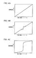
- Figs. 4A through 4C illustrate the current-voltage (I-V) characteristic across the junction varying with different thickness of the Josephson junctions.
- first and second superconductors are made of the same superconductor material as the example shown in Fig. 3 , FF type I-V characteristic is likely to result since the first and second superconductors have high affinity with each other so that the first and second superconductors may be short circuited across the interface of the junction at some points if the conditions of forming the second superconductor are similar to those of the first superconductor.
- I-V characteristic of a junction may be made less likely to become FF type by forming the first and second superconductors from materials of different compositions, thereby causing the first and second superconductors to have less affinity with each other.
- the superconductors When the first and second superconductors are formed from materials of different compositions, the superconductors have different intervals between CuO 2 planes, that are major transmission paths in the high temperature superconductors, in the c-axis direction, so that the CuO 2 planes of the first and second superconductors become less compatible to each other at the junction, and the junction should be less likely to have FF type I-V characteristics as shown in Fig. 5 .
- second superconductor/first superconductor as YBa 2 Cu 3 O y /NdBa 2 Cu 3 O y , YbBa 2 Cu 3 O y /YBa 2 Cu 3 O y , Y(Ba, La) 2 Cu 3 O y /YBa 2 Cu 3 O y , and YBa 2 Cu 3 O y /Y(Ba, La) 2 Cu 3 O y have been tried.
- a physical film forming process such as sputtering process or laser deposition process does not offer process conditions having large margins that allow it to form a c-axis orientation film that is good in all respects including superconductivity, surface flatness and crystallinity, which are related to achieving high quality of superconductor film.
- the upper and lower electrodes are formed while seeking trade-off points, in the actual film forming process.
- the most important portion of a Josephson junction, ramp-edge type Josephson junction in particular, is a layer as thin as 1 to 2 nm where the first and second superconductors make contact, and reliability of the product device depends on establishing the technology to form this portion with good reproducibility. Actually, however, the conditions for reliably forming the desired junction have not been clarified.
- junction layer When the junction layer is too thick, superconducting current cannot flow and therefore the junction shows current-voltage characteristic (I-V characteristic) of a resistive material as shown in Fig. 4A .
- Producing a superconducting electronic device that employs the Josephson effect requires it to form a number of Josephson junctions that show the RSJ characteristic described above and have appropriate values of critical current Ic and IcRn product. At present, however, there is significant variance among the Josephson junctions, and satisfactory levels of stability of characteristics and reliability have not been achieved.
- J. Talvacchio et al for example, in order to have a circuit consisting of 100 junctions or more to operate, variations in the characteristics represented in terms of the proportion (percentage) of standard deviation ( ⁇ ) of the value of the characteristic in question to the mean value of the characteristic (X) must be controlled to within 10% (100 ⁇ /X ⁇ 10) ( J. Talvacchio et al., IEEE Trans. Appl. Supercond. 7, 2051 (1997 )). A successful case of achieving this requirement for ramp-edge type Josephson junction has recently been reported.
- Saotome et al. achieved a standard deviation ( ⁇ ) of 7.9% at 4.2K for 100 junctions made by using YBa 2 Cu 3 O y-x for the superconductor electrode and CeO 2 for the insulation layer ( Soutome et al., Proceedings of 62nd Academic Lecture Conference of The Japanese Applied Physics Society, No. 1, p. 195 14a-G-7 (2001, 9/11-14 )). They did not use any material that included La, and achieved the value described above with such a structure and a process in which La does not mix in between the two superconducting electrodes.
- a first object of the present invention is to provide a Josephson junction, particularly a ramp-edge type Josephson junction and an electronic device provided with the Josephson junction of high performance and high reliability that can be made easily and reliably under film forming conditions with generous margins for error by solving the first problem described above, and further to provide a method of manufacturing the Josephson junction conveniently.
- a second object of the present invention is to provide a high temperature superconducting Josephson junction that allows less variations among a plurality of Josephson junctions and enables it to improve the characteristics and reliability of a product that employs the Josephson junction, and to provide a superconducting electronic device that incorporates the high temperature superconducting Josephson junction.
- First aspect of the present invention has been conceived on the basis of the findings described above, and provides the Josephson junction, a method of manufacturing the Josephson junction and an electronic device provided with the Josephson junction as follows.
- the barrier layer of the Josephson junction preferably includes cations with ionic radius in the case of being 6-coordinated with oxygen (O), of 0.0947 nm or larger in a concentration of 35 to 65% in terms of cation atom ratio. This causes the perovskite structure that has good affinity with the first and second superconductors to be stabilized so as to form a uniform barrier layer.
- the barrier layer is preferably joined with the two superconductors through ramp-edge junction or stacked junction.
- Structure of the Josephson junction can be materialized in "ramp-edge junction” and "stacked junction”.
- the superconducting electronic device is characterized in that at least one high temperature superconducting Josephson junction according to the first aspect of the present invention is provided therein.
- the present invention provides a Josephson junction that has high reliability and high performance by properly controlling the composition of the superconductor material, and makes it possible to manufacture a high performance Josephson junction with high efficiency in stable conditions by improving the way elements are supplied when forming the superconductor layers.
- the present invention will be described in detail below together with the operation thereof.
- the Josephson junction according to the present invention is made by forming the first superconductor and the second superconductor from a high temperature superconductor material made up of A (one or more element selected from a group of La, Nd, Sm, Eu, Gd, Dy, Ho, Er, Tm, Yb, Lu and Y), B (one or more element selected from a group of Ba, Sr and Ca), Cu and oxygen, while the first superconductors and the second superconductor are constituted from five or more elements and have compositions differing from each other.
- A one or more element selected from a group of La, Nd, Sm, Eu, Gd, Dy, Ho, Er, Tm, Yb, Lu and Y
- B one or more element selected from a group of Ba, Sr and Ca
- Cu and oxygen while the first superconductors and the second superconductor are constituted from five or more elements and have compositions differing from each other.
- the constitution described above increases the degree of freedom with regards to the material so as to make it possible to manufacture the high-quality Josephson junction within the restraints of the film forming apparatus, and makes it easier to control the properties of the Josephson junction.
- composition of the film material is one of the most important factors.
- a copper oxide superconductor includes cations of A, Ba and Cu disposed regularly.
- the disparity in the composition results in a lattice defect in the crystal that constitutes the film, thereby straining the crystal.
- the strain not only appears on the surface in the form of bulges or dents resulting in impaired surface flatness, but also disturbs the crystal orientation, thus affecting adversely the film properties.
- existence of the disparity in the composition described above also causes the excess component to precipitate on the film surface when forming the film, again impairing the surface flatness of the film and resulting in degradation in the properties.
- the copper oxide superconductor When the copper oxide superconductor is constituted from five or more elements, a superconductor without impurity included therein can be formed even when the process conditions vary somewhat during formation of the superconductor. This is because the elements other than Cu and oxygen can occupy the element site of each other in the crystal structure.
- the Josephson junction is made of a 4-element superconductor material, for example YBa 2 Cu 3 O y , then the ratio of Y to Ba must not be other than 1:2 and deviation of the composition from this ratio immediately materializes in the form of impurity precipitation.
- the component Y is completely or partially replaced with one or more element selected from the group of La, Nd, Sm, Eu, Gd, Dy, Ho, Er, Tm, Yb and Lu, or element Ba is completely or partially replaced with Sr and/or Ca so as to make a constitution of five or more elements
- the only condition to be satisfied is that the total number of atoms of the elements other than Cu and oxygen is equal to the number of Cu atoms.
- regular arrangement is attained without causing lattice defects or precipitation of impurity.
- the degree of freedom in the composition is increased in that some margins are allowed for the proportions of the elements other than Cu and oxygen to deviate. This is an advantage not found in the 4-element superconductor material YBa 2 Cu 3 O y where the ratio of Y to Ba must not be other than 1:2.
- the greater degree of freedom in the material composition of the superconductor constituted from five or more elements significantly relaxes the restrictions on the film forming conditions, so as to make it possible to manufacture varieties of Josephson junction in order to meet the restraints of the film forming apparatus and the required product characteristics. That is, the film forming conditions can be controlled so as to form a satisfactory c-axis orientation film of superconductor also by constituting the superconductor from five or more elements and adjusting the composition of the superconductor material to clear the restraints of the film forming apparatus.
- high-quality Josephson junctions can be manufactured simply by changing the element source (target) of properly controlled composition when forming superconductor thin film, in spite of restraints of the film forming apparatus.
- Formation of the second superconductor layer of the Josephson junction must be carried out under such conditions that do not deteriorate the first superconductor layer that has already been formed.
- An important parameter with this regard is the substrate temperature (film forming temperature), and it is desired that film forming temperature for the second superconductor layer be lower than that of the first superconductor layer. This requirement can be met without leading to lower performance when the superconductor is constituted from five or more elements. This is because constituting the superconductor from five or more elements allows for a margin of error in controlling the film forming temperature.
- the Josephson junction according to the first aspect of the present invention can be made with as high a quality as is permitted by the restraints of the film forming apparatus. Properties of the Josephson junction may also be controlled during the process.
- multiple-element constitution of the superconductor material that makes the Josephson junction namely constitution from five or more elements, also has an effect of increasing the IcRn product.
- the high temperature superconducting Josephson junction is made by a physical film forming process with a plurality of element sources (targets) disposed in the airtight film forming chamber and the plurality of element sources are switched as required so as to form the upper and lower superconductor layers of different compositions each including at least five elements, composition of the thin film can be easily controlled over a wide range without replacing the element sources (targets) in the film forming chamber.
- the invention makes it possible to form the thin film of controlled composition easily without opening the airtight film forming chamber to the atmosphere to change the element source (target), by providing the plurality of element sources (targets) disposed in the airtight film forming chamber and depositing the particles of the elements on a substrate through plasma or laser irradiation while switching the plurality of element sources and making an arrangement for the control of the amount of particles supplied from each element source.
- the present inventors reached the following finding. That is, stability can be improved without compromising the characteristics and therefore variability in the characteristics among chips can be restrained when the barrier layer includes one or more elements selected from the group of La, Nd, Sm and Eu, and one or more elements selected from the group of Y, Gd, Dy, Ho, Er, Tm, Yb and Lu, and preferably cations that have ionic radius in case of being 6-coordinated with oxygen being 0.0947 nm or larger are included in a concentration of 35 to 65% in terms of cation atom ratio.
- the high temperature superconducting Josephson junction according to the second aspect of the present invention is a Josephson junction having a barrier layer sandwiched by two superconductors wherein the superconductors include one or more elements (RE) selected from the group of Y, La, Nd, Sm, Eu, Gd, Dy, Ho, Er, Tm, Yb and Lu, one or more elements (AE) selected from the group of Ba, Sr and Ca, and Cu and oxygen (O), while the barrier layer includes one or more elements (RE1) selected from the group of La, Nd, Sm and Eu, and one or more elements (RE2) selected from the group of Y, Gd, Dy, Ho, Er, Tm, Yb and Lu.
- the superconductors include one or more elements (RE) selected from the group of Y, La, Nd, Sm, Eu, Gd, Dy, Ho, Er, Tm, Yb and Lu, one or more elements (RE2) selected from the group of Y, Gd, Dy, Ho, Er, Tm
- the barrier layer preferably includes cations that have ionic radius in the case of being 6-coordinated with oxygen (O) being 0.0947 nm or larger in a concentration of 35 to 65% in terms of cation atom ratio. This causes the perovskite structure that has good affinity with the first and second superconductors to be stabilized so as to form a uniform barrier layer.
- the barrier layer is preferably joined with the two superconductors through a ramp-edge junction or a stacked junction.
- the structure of the Josephson junction can be formed as a ramp-edge junction or a stacked junction.
- the present invention provides a superconducting electronic device that is provided with at least one high temperature superconducting Josephson junction according to the second aspect of the present invention.
- the barrier layer located at the junction interface is said to be in a crystal phase that has a perovskite structure of thickness as small as about 2 nm.
- the perovskite structure is represented by chemical formula ABO 3 , that has such a structure as an atom located at site A (atom A) is surrounded by twelve oxygen atoms and an atom located at site B (atom B) is surrounded by six oxygen atoms.
- a cation having a relatively large ionic radius occupies site A and a cation having small ionic radius occupies site B.
- Y atoms may occupy the 12-coordinate sites, and Y may precipitate in the form of stable phase such as Y 2 O 3 . Precipitation of such a different phase causes degradation in controllability and reliability of the characteristics of Josephson junctions.
- the barrier layer takes on a perovskite structure represented by Y 1-x BaCu x O y (x ⁇ 0.5, y ⁇ 3) with lattice constant in a range from 0.41 to 0.43 nm.
- Investigation of the composition by means of analytical type transmission electron microscope revealed that the proportion of Ba: Y + Cu deviated from 1:1.
- Y atoms that cannot occupy site A would precipitate in the form of Y 2 O 3 .
- Lattice constant of YBa 2 Cu 3 O y high-temperature superconductor is a ⁇ b ⁇ c/3 ⁇ 0.38 - 0.39 nm, that is less than 0.41 - 0.43 nm.
- the barrier layer includes one or more elements (RE1) selected from the group of La, Nd, Sm and Eu, and one or more elements (RE2) selected from the group of Y, Gd, Dy, Ho, Er, Tm, Yb and Lu
- the element (RE1) that constitutes the barrier layer is, since this element has a relatively large ionic radius among the elements (RE) that constitute the superconductor, it is likely to occupy site A of the perovskite structure.
- the element (RE2) that constitutes the barrier layer is likely to occupy site B of the perovskite structure.
- the two superconductor layers each include five elements and have compositions different from each other. This increases the margins of error for the process conditions that allow it to form a c-axis orientation film that is good in all respects including superconductivity, surface flatness and crystallinity, thus making it easier to form the thin superconductor film that has high quality.
- a Josephson junction that uses a layer damaged during processing (damaged layer produced when cutting the ramp edge plane of the first superconductor), too, the I-V characteristic can be easily made to that of RSJ type, and Josephson junctions having a large value of IcRn product and high reliability can be obtained.
- Fig. 1 is a sectional view of a high temperature superconducting Josephson junction of the ramp-edge type according to a first embodiment of the present invention.
- reference numeral 1 denotes a substrate
- 2 denotes a first superconductor
- 3 denotes an inter-layer insulation film
- 4 denotes a second superconductor
- 5 denotes a barrier layer.
- the first superconductor 2 is processed at an edge thereof so as to form an edge face 2a inclined by a predetermined angle from the surface of the substrate 1.
- the inter-layer insulation film 3 is also processed to form an edge face inclined against the substrate 1, namely, an edge face 3a lying in the same plane as the edge face 2a of the first superconductor 2.
- the second superconductor 4 is formed so as to cover the first superconductor 2 and the inter-layer insulation film 3 as a whole in the Josephson junction.
- An extremely thin barrier layer 5 is formed in the interface between the second superconductor 4 and the edge face 2a of the first superconductor 2.
- the ramp-edge type Josephson junction of such a structure is made as the barrier layer 5 is sandwiched by two superconductors 2 and 4.
- the substrate 1 is an insulating substrate with an extremely flat surface and is preferably made of an inorganic insulating material such as (La 0.3 Sr 0.7 )(Al 0.65 Ta 0.35 )O 3 , MgO, SrTiO 3 (STO), NdGaO 3 or LaAlO 3 .
- an inorganic insulating material such as (La 0.3 Sr 0.7 )(Al 0.65 Ta 0.35 )O 3 , MgO, SrTiO 3 (STO), NdGaO 3 or LaAlO 3 .
- the first superconductor 2 and the second superconductor 4 are made of copper oxide high temperature superconductor, that is a ceramic material of perovskite structure that includes one or more elements (Re) selected from among the group of Y, La, Nd, Sm, Eu, Gd, Dy, Ho, Er, Tm, Yb and Lu, one or more elements (Ae) selected from the group of Ba, Sr and Ca, and Cu and oxygen (O).
- Re copper oxide high temperature superconductor
- composition of the first superconductor 2 and the second superconductor 4 are required only to satisfy the requirements described above.
- Y 3-x-y Ba x La y Cu 3 O z YBLCO
- YBa 2 Cu 3 O z YBCO
- NdBa 2 Cu 3 O 2 NdBCO
- YbBa 2 Cu 3 O y YbBCO
- Yb 3-x-y Ba x La y Cu 3 O 2
- the inter-layer insulation film 3 is made of an insulating material that can insulate between the first superconductor 2 and the second superconductor 4, and such materials are preferably used as CeO 2 , (La 0.3 Sr 0.7 )(Al 0.65 Ta 0.35 )O 3 , SrTiO 3 (STO) or CaSnO 3 .
- the barrier layer 5 is an extremely thin layer made of an oxide compound having a composition different from those of the first superconductor 2 and the second superconductor 4 and includes one or more elements (RE1) selected from the group of La, Nd, Sm and Eu, and one or more elements (RE2) selected from the group of Y, Gd, Dy, Ho, Er, Tm, Yb and Lu.
- elements RE1 selected from the group of La, Nd, Sm and Eu
- RE2 elements selected from the group of Y, Gd, Dy, Ho, Er, Tm, Yb and Lu.
- Y 3-x-y Ba x La y Cu 3 O w (YBLCO), (Y, Yb) 1-x-y z Ba x La y Cu 2 O w or Nd 1-x-y-z Y x Ba y Cu z O w is preferably used, where x, y, z and w take values that stabilize the crystal structure based on perovskite structure.
- the barrier layer includes cations with ionic radius in case of being 6-coordinated with oxygen (O) 0.0947 nm or larger in a concentration of 35 to 65% in terms of cation atom ratio, and the oxygen content w is a value that is sufficient to maintain the perovskite structure.
- the barrier layer 5 may include alkali metal, transition metal or other elements added by such a technique as artificial barrier.
- the barrier layer preferably includes cations that have ionic radius in case of being 6-coordinated with oxygen (O) 0.0947 nm or larger in a concentration of 35 to 65% in terms of cation atom ratio.
- Composition of the barrier layer can be quantitatively analyzed by using an analytical type transmission electron microscope with electron beam about 1 nm in diameter or less. Ionic radius given in this embodiment, however, is determined by making reference to Shannon's paper ( R.D. Shannon, Acta Cryst. A32 p.751 (1976 )).
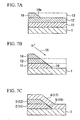
- a first superconductor layer 11 and an inter-layer insulation film 12 are formed successively on the substrate 1 by RF sputtering process, CVD process, reactive CVD process or the like, and then a photo-resist layer 13 is formed on the inter-layer insulation film 12 by spin coating process or the like.
- the photo-resist layer 13 is patterned by photolithography, and reflow processing is applied to the patterned photo-resist, thereby to form the mask 14 having an edge 14a that is gently inclined.
- the mask 14 is used to etch the inter-layer insulation film 12 and the first superconductor layer 11 with Ar ion (Ar + ) bombardment 15, so as to form gently inclined surfaces at the edges of the inter-layer insulation film 12 and the first superconductor layer 11 of the Josephson junction.
- Ar ion (Ar + ) bombardment 15 the ramp surface of the first superconductor layer 11 is damaged by the Ar ion (Ar + ) bombardment 15 to form an extremely thin damaged layer 16.
- the mask 14 is then removed by means of an ashing apparatus.
- a second superconductor layer 17 is formed on the first superconductor layer 11 and the inter-layer insulation film 12 by laser deposition or the like.
- the damaged layer 16 produced on the ramp surface of the first superconductor layer 11 reacts with the first superconductor layer 11 and the second superconductor layer 17, so as to turn into the barrier layer 5.
- electrodes are formed from an electrically conductive material such as gold (Au) by vapor deposition or sputtering process, at predetermined positions on the first superconductor layer 11 and the second superconductor layer 17.
- Au gold
- the ramp-edge type Josephson junction having the extremely thin barrier layer 5 sandwiched between the two superconductors 2 and 4 can be easily made by using the IEJ technique.
- the barrier layer 5 includes one or more elements (RE1) selected from the group of La, Nd, Sm and Eu, and one or more elements (RE2) selected from the group of Y, Gd, Dy, Ho, Er, Tm, Yb and Lu, the element (RE1) is likely to occupy site A and the element (RE2) is likely to occupy site B, so that stability of the barrier layer 5 can be improved.
- elements (RE1) selected from the group of La, Nd, Sm and Eu
- elements (RE2) selected from the group of Y, Gd, Dy, Ho, Er, Tm, Yb and Lu
- the barrier layer 5 includes the element (RE1) and the element (RE2), lattice matching between the barrier layer 5 and the two superconductors 2 and 4 can be improved, thereby producing a more stable Josephson junction.
- Fig. 2 is a sectional view of the stacked type high temperature superconducting Josephson junction according to the second embodiment of the present invention.
- the first superconductor 2 and the inter-layer insulation film 3 are formed successively on the substrate 1, the opening 3b is formed in the inter-layer insulation film 3 at a position where a Josephson junction is to be made, the second superconductor 4 is formed on the inter-layer insulation film 3 and on the first superconductor 2 that is exposed through the opening 3b, and the damaged layer produced by bombarding Ar ions (Ar + ) on the surface of the first superconductor 2 that is exposed through the opening 3b reacts with the first superconductor 2 and the second superconductor 4 so as to turn into the extremely thin barrier layer 5.
- Ar + Ar ions
- the Josephson junction of this embodiment has a structure different from that of the Josephson junction of the first embodiment described previously.
- the Josephson junction of this embodiment can be easily made by an IEJ technique similarly to the Josephson junction of the first embodiment.
- the stacked type high temperature superconducting Josephson junction of this embodiment can also achieve exactly the same effect as that of the ramp-edge type high temperature superconducting Josephson junction of the first embodiment.
- the Josephson junction is of an IEJ type wherein the layer damaged during processing is used as the junction, as shown in Fig. 1 , while formation of such a ramp-edge type Josephson junction was attempted as the variance ( ⁇ /X) was restrained within 10% and critical current Ic is 1.0 mA or higher (4.2K). 25 Pieces of the device were made for each test.
- the inter-layer insulation film of (La,Sr) 2 AlTaO 6 (LSAT) was formed to a thickness of 200 nm under the same conditions on the first superconductor made of YBa 2 Cu 3 O y .
- the second superconductor made of YBa 2 Cu 3 O y was formed to a thickness of 200 nm by laser deposition.
- oxygen was introduced at a pressure of 26.7 Pa (200 mTorr) and the YBa 2 Cu 3 O y target having stoichiometrical composition was irradiated with laser beam of 400 mJ output. Energy density of the laser beam on the target was 1.5 J/cm 2 .
- the junction made under the conditions of 60 mm for the distance between the substrate and the target and 690 to 710°C for the substrate temperature (film forming temperature) showed RSJ type I-V characteristic at 4.2K.
- I-V characteristic, Ic and IcRn product measured on ramp-edge type Josephson junctions made with different film forming temperatures (substrate temperatures) for the second superconductor are shown in Table 1.
- Table 1 Second superconductor layer forming temperature (°C)
- I-V characteristic, Ic and IcRn product measured on the ramp-edge type Josephson junctions made with the above materials used for the second superconductor are shown in Table 2.
- Table 2 Second superconductor layer forming temperature (°C) I-V characteristic Critical current Ic (mA) IcRn (mV) 740 FF - - 730 RSJ 1.0 2.0 720 RSJ 1.1 2.1 710 RSJ 0.8 2.0 700 RSJ 0.6 1.3 690 Resistor - - 680 Resistor - -
- a Y 0.9 Ba 1.9 La 0.2 Cu 3 O y film was formed to a thickness of 200 nm for the first superconductor on the substrate by off-axis high frequency sputtering process.
- a c-axis orientation film having flat surface was obtained when the substrate temperature was 750°C.
- the inter-layer insulation film of (La,Sr) 2 AlTaO 6 (LSAT) was formed to a thickness of 200 nm with a technique similar to that of the comparative test on the first superconductor layer made of Y 0.9 Ba 1.9 La 0.2 Cu 3 O y that was formed as described above.
- LSAT Layer-layer insulation film
- patterning was carried out by photolithography, and the ramp surface of the first superconductor was formed by applying Ar ion bombardment (acceleration voltage 500 V) at an angle of 30°.
- ramp-edge type Josephson junction was completed by forming a YBa 1.7 Sr 0.3 Cu 3 O y film to a thickness of 200 nm by laser deposition (substrate temperature 720°C) for the second superconductor.
- the value of Ic tended to decrease when the temperature of forming the second superconductor was reduced, similarly as shown by the data of Table 1 for Example 1. For this reason, the YBa 2 Cu 3 O y film for the second superconductor was formed at 680°C, hoping to achieve an Ic of 0.5 mA. However, a resistor resulted instead of a Josephson junction.
- the second superconductor was made from a thin YbBa 2 Cu 3 O y film that allows it to form a c-axis orientation film at a lower temperature than in the case of YBa 2 Cu 3 O y , and the c-axis orientation film was obtained when the substrate temperature (film forming temperature) was in a range from 650 to 680°C.
- I-V characteristic, Ic and IcRn product measured on the ramp-edge type Josephson junctions made with the above materials used for the second superconductor are shown in Table 3.
- Table 3 Second superconductor layer forming temperature (°C) I-V characteristic Critical current Ic (mA) Ic (mA) IcRn (mV) 690 FF - - 680 FF - - 670 RSJ 0.4 1.7 660 RSJ 0.2 1.4 650 Resistor - -
- the process of forming the Josephson junction was closely examined. Although the X-ray diffraction analysis of the YBa 2 Cu 3 O y film of the second superconductor showed c-axis orientation, observation with an optical microscope revealed that the surface was very rough so that contrast could easily be obtained.
- the second superconductor layer was formed from Yb 0.9 Ba 1.9 Nd 0.2 Cu 3 O y made by replacing Yb and Ba in YbBa 2 Cu 3 O y with a small amount of Nd that can partially substitute the atomic sites of both Yb and Ba, by laser deposition at the substrate temperature (film forming temperature) of 670°C.
- Example 1 and Example 2 were conducted in the conventional manner, but it is very tedious to open the airtight film forming chamber (vacuum chamber) to the atmosphere and replace the target material, in order to achieve the target characteristics.
- Fig. 8 schematically shows the target stage of the laser deposition film forming apparatus used in the example.
- Placed on the target stage are three target materials of SmBa 2 Cu 3 O y , YBa 2 Cu 3 O y and YbBa 2 Cu 3 O y , the target stage being rotated so as to select the target material to be irradiated with a laser beam and to control the duration and the number of irradiations, thereby to control the composition of the superconductor film of solid solution system to be formed on the substrate.
- This control over the composition of the superconductor film to be formed also enables it to control the substrate temperature that allows it to yield a c-axis orientation film that has a flat surface.
- the film forming temperature (substrate temperature) at which the c-axis orientation film can be made by laser deposition is from 750 to 780°C for SmBa 2 Cu 3 O y , from 700 to 730°C for YBa 2 Cu 3 O y , and from 650 to 680°C for YbBa 2 Cu 3 O y , and therefore the c-axis orientation film can be made at a temperature in a range from 700 to 780°C for (Sm, Y)Ba 2 Cu 3 O y , and from 650 to 730°C for (Y, Yb)Ba 2 Cu 3 O y .
- the ramp-edge type Josephson junctions having various combinations of the second superconductor layer and the first superconductor layer of different compositions were manufactured by placing the three kinds of target material in the vacuum chamber of the film forming apparatus, while setting the film forming temperature (substrate temperature) from 700 to 780°C when forming the first superconductor layer, and setting the film forming temperature (substrate temperature) from 650 to 730°C when forming the second superconductor layer without opening the vacuum chamber to the atmosphere and changing the target material.
- junctions having critical current Ic of 0.5 mA, 1.0 mA, 1.5 mA and 2.0 mA are represented by tests Nos. 19, 10, 7 and 3.
- junctions having critical current Ic of 0.7 mA are represented by tests Nos. 14 and 18, they have different values of IcRn, namely, 2.1 mV and 3.1 mV. This means that junctions having different values of IcRn can be made even when Ic is the same, by changing Ln.
- the Josephson junctions are of the IEJ type wherein the layer damaged during processing is used as the junction, while formation of ramp-edge type Josephson junctions having the same critical current Ic of about 1.0 mA (4.2K) but different values of IcRn was attempted.
- the junction device comprising the second superconductor and the first superconductor made of YBa 1.7 Sr 0.3 Cu 3 O y and Y 0.9 Ba 1.9 Sr 0.2 Cu 3 O y , respectively, manufactured in Example 1 showed critical current Ic of 1.2 mA and IcRn product of 2.2 mV.
- ramp-edge type Josephson junctions with the second superconductor changed to a multiple-component material of Gd 0.5 Tm 0.5 Ba 1.7 Sr 0.3 Cu 3 O y or Eu 0.5 Lu 0.5 Ba 1.7 Sr 0.3 Cu 3 O y .
- Mean ionic radius of Gd and Tm and mean ionic radius of Eu and Lu are similar to the ionic radius of Y.
- Ramp-edge type Josephson junction was manufactured by using Y 0.9 Ba 1.9 La 0.2 Cu 3 O y for the first superconductor, Y 0.95 Ba 1.95 La 0.1 Cu 3 O y for the second superconductor and (La 0.3 Sr 0.7 )(Al 0.65 Ta 0.35 )O 3 (hereinafter referred to as LSAT) for the substrate by using the IEJ technique.
- the first superconductor was formed on a LSAT substrate by the off-axis high frequency sputtering process, and an inter-layer insulation film of LSAT was formed thereon, both to thicknesses of 200 nm. Then, the inter-layer insulation film was coated with photo-resist by a spin coating process, with the photo-resist film being patterned by photolithography, and reflow process was applied so as to form a gentle slope at the edge. Then, the inter-layer insulation film and the first superconductor were etched by Ar ions applied with acceleration voltage of 400 V and ion current 50 mA. Bombardment of Ar ions was carried out while rotating the substrate with the ion beam inclined by 30° from the substrate surface.
- Example 1 The samples of Example 1 were made by further depositing gold (Au) and forming an electrode of predetermined shape through proper patterning.
- Observation of the barrier layer with an analytical type transmission electron microscope having an electron beam of about 1 nm diameter showed that thickness of the barrier layer was 1 nm or less at most points.
- Atoms having ionic radius in the case of being 6-coordinated with oxygen of 0.0947 nm or larger were Ba and La which accounted for 51% in terms of cation atom ratio.
- Ramp-edge type Josephson junctions were manufactured by the IEJ technique using YBa 2 Cu 3 O y for the first superconductor and the second superconductor.
- the first superconductor layer was formed on a LSAT substrate and an inter-layer insulation film of LSAT was formed thereon, both to thicknesses of 200 nm, by the off-axis high frequency sputtering process. Then, gentle slopes were formed on the inter-layer insulation film and the first superconductor layer similarly to Example 1, and second superconductor layer was formed thereon.
- Ramp-edge type Josephson junctions were manufactured by using Y 0.9 Ba 1.9 La 0.2 Cu 3 O y for the first superconductor and Yb 0.9 Ba 1.9 La 0.2 Cu 3 O y for the second superconductor by using the IEJ technique.
- the substrate was made of MgO and the inter-layer insulation film was made of CeO 2 .
- Ramp-edge type Josephson junction was manufactured by the IEJ technique similarly to Example 6, except for using YBa 2 Cu 3 O y that does not include La for the first superconductor.
- Atoms having ionic radius in the case of being 6-coordinated with oxygen of 0.0947 nm or larger was Ba which accounted for 34% in terms of cation atom ratio.
- Ramp-edge type Josephson junctions were manufactured by using Nd 0.9 Ba 1.9 La 0.2 Cu 3 O y for the first superconductor layer and Y 0.9 Ba 1.9 La 0.2 Cu 3 O y for the second superconductor layer, by the artificial barrier technique that formed a thin Y 2 Cu 2 O 5 film before forming the second superconductor layer.
- the first superconductor layer was formed on a substrate made of MgO and an inter-layer insulation film made of CeO 2 was formed thereon, each to a thickness of 200 nm by the off-axis high frequency sputtering process. Then similarly to Example 1, the inter-layer insulation film and the first superconductor were processed to form a gentle slope. A Y 2 Cu 2 O 5 film about 3 nm thick was formed thereon by laser deposition, and further over which the second superconductor layer was formed.
- Ramp-edge type Josephson junctions were manufactured by the IEJ technique similarly to Example 3, although the process of forming the Y 2 Cu 2 O 5 film was omitted.
- junctions formed on the substrate four junctions showed I-V characteristics of the FF type, not a Josephson junction. The remaining six showed I-V characteristics of the RSJ type, indicating they were Josephson junctions.
- Ramp-edge type Josephson junction was manufactured by artificial barrier technique similarly to Example 7, except for using Y 0.2 Nd 0.9 Ba 1.9 Cu 3 O y for the first superconductor layer and Y 0.9 Nd 0.2 Ba 1.9 Cu 3 O y for the second superconductor layer, while forming a thin Y 2 BaCuO 5 film before forming the second superconductor layer.
- Ten Josephson junctions formed on the substrate all showed I-V characteristics of the RSJ type. They also showed IcRn product in a range from 2.1 to 2.5 mV at 4.2K, and critical current Ic of about 1.0 mA. Upon measurement of critical current Ic of 100 Josephson junctions connected in series on a substrate, the critical current Ic showed variance ( ⁇ /X) of 7.3%.
- Ramp-edge type Josephson junction was manufactured by the artificial barrier technique similarly to Example 8, except for forming Nd 4 Ba 2 Cu 2 O 10 film instead of the Y 2 BaCuO 5 before forming the second superconductor layer.
- junctions formed on the substrate three junctions showed I-V characteristic of FF type, not Josephson junction. The remaining seven showed I-V characteristics of the RSJ type, indicating they were Josephson junctions.
- Atoms having ionic radius in the case of being 6-coordinated with oxygen of 0.0947 nm or larger were Nd and Ba which accounted for 66% in terms of cation atom ratio.
- Stacked type superconducting Josephson junctions were manufactured by using Y 0.9 Ba 1.9 La 0.2 Cu 3 O y for the first superconductor and Yb 0.9 Ba 1.9 La 0.2 Cu 3 O y for the second superconductor by using the IEJ technique.
- the substrate was made of MgO and the inter-layer insulation film was made of CeO 2 .
- the first superconductor layer and the inter-layer insulation film were formed by off-axis high frequency sputtering processes both to thickness of 200 nm. Then, the inter-layer insulation film was coated with photo-resist by a spin coating process, with the photo-resist film being patterned by photolithography so as to make a mask. Then the inter-layer insulation film was etched by Ar ions applied with acceleration voltage of 400 V and ion current 50 mA using the mask, thereby to form an opening in the inter-layer insulation film at a position where the Josephson junction is to be formed.
- the exposed surface of the first superconductor is covered with a damage layer caused by Ar ion bombardment. With the remaining resist being removed by means of an ashing apparatus, the second superconductor layer was formed on the inter-layer insulation film and the first superconductor by laser deposition process.
- Ten Josephson junctions formed on the substrate all showed I-V characteristics of the RSJ type. These Josephson junctions also showed IcRn product in a range from 1.2 to 1.6 mV at 4.2K, and critical current Ic of about 0.3 mA. Measurement of critical current Ic of ten Josephson junctions formed on a substrate showed variance ( ⁇ /X) of 9.8%.
- Atoms having ionic radius in the case of being 6-coordinated with oxygen of 0.0947 nm or larger were Ba and La which accounted for 47% in terms of cation atom ratio.
- Ramp-edge type Josephson junctions were manufactured by using Y 0.9 Nd 0.2 Ba 1.9 Cu 3 O y for the first superconductor layer and Y 0.95 Nd 0.1 Ba 1.95 Cu 3 O y for the second superconductor layer, by the artificial barrier technique that formed a thin Nd 2 CuO 4 film before forming the second superconductor layer.
- thickness of the Nd 2 CuO 4 film was changed to study the effect of the thickness on the Josephson junction.
- the first superconductor layer was formed on a substrate made of MgO and an inter-layer insulation film made of CeO 2 was formed thereon, each to a thickness of 200 nm by the off-axis high frequency sputtering process. Then, similarly to Example 1, the inter-layer insulation film and the first superconductor were processed to form a gentle slope. Nd 2 CuO 4 films having thicknesses ranging from about 0.5 to 50 nm were formed by laser deposition, whereon the second superconductor layer was then formed.
- I-V characteristic, critical current Ic, variance ⁇ /X of critical current Ic and ratio (Nd + Ba):(Y + Cu) were determined for each sample, with the data shown in Table 6.
- the I-V characteristics and critical currents Ic were measured on ten Josephson junctions formed on the substrate. I-V characteristics are indicated in the table as FF, RSJ or resistor.
- the variance ⁇ /X was determined from measurements of critical current Ic of 100 Josephson junctions formed on the same substrate at 4.2K. Table 6 Sample No.
- Table 6 shows that I-V characteristics of the RSJ type is obtained when thickness of the Nd 2 CuO 4 film is in a range from 1 to 20 nm, and the variance ⁇ /X becomes less than 10% when the thickness is in a range from 2 to 5 nm. It was also found that samples that are from 2 to 3 nm thick, in particular, show I-V characteristics of the RSJ type with variance ⁇ /X less than 8%, thus showing the effect of suppressing the variability in characteristics.
- the two superconductors that interpose the barrier layer include one or more elements selected from the group of Y, La, Nd, Sm, Eu, Gd, Dy, Ho, Er, Tm, Yb and Lu, one or more elements selected from the group of Ba, Sr and Ca, and Cu and oxygen (O), so that each of the two superconductors include at least five elements of different composition from each other.
- This constitution enables control of the characteristics of the junction, and provides a Josephson junction of high reliability that can meet the requirements for the design of various circuits, on a stable basis, for ease of operation.
- the superconductors that interpose the barrier layer include one or more elements (RE) selected from the group of Y, La, Nd, Sm, Eu, Gd, Dy, Ho, Er, Tm, Yb and Lu, one or more elements (AE) selected from the group of Ba, Sr and Ca, and Cu and oxygen (O), while the barrier layer includes one or more elements (RE1) selected from the group of La, Nd, Sm and Eu, and one or more elements (RE2) selected from the group of Y, Gd, Dy, Ho, Er, Tm, Yb and Lu.
- RE elements selected from the group of Y, La, Nd, Sm, Eu, Gd, Dy, Ho, Er, Tm, Yb and Lu.
- This constitution improves the lattice matching between the barrier layer and the two superconductors, thus achieving more stable Josephson junctions.
- a Josephson junction can be provided that has good RSJ characteristics, and has extremely small variance in the critical current Ic and in IcRn product.
- the superconducting electronic device of the present invention that has one or more high temperature superconducting Josephson junctions of the first aspect of the present invention has the Josephson junctions of high reliability that can meet the requirements imposed by the design of various circuits.
- the superconducting electronic device of the present invention that has one or more high temperature superconducting Josephson junctions of the second aspect of the present invention allows it to suppress the variability in the characteristics of the Josephson junctions provided in a superconducting electronic device to a low level, thus improving the electrical characteristics and reliability of the superconducting electronic device. As a result, electrical characteristics and reliability of the product that uses the superconducting electronic device can be improved.
- the present invention has very high significance to the industry.
Landscapes
- Engineering & Computer Science (AREA)
- Chemical & Material Sciences (AREA)
- Ceramic Engineering (AREA)
- Manufacturing & Machinery (AREA)
- Superconductor Devices And Manufacturing Methods Thereof (AREA)
- Oxygen, Ozone, And Oxides In General (AREA)
Claims (6)
- Hochtemperatursupraleitender Josephson-Kontakt, aufweisend eine Sperrschicht (5), die zwischen zwei Supraleiter-Schichten (2, 4) liegend angeordnet ist, wobei jede Supraleiter-Schicht zumindest fünf Elemente aufweist, die ausgewählt sind aus(a) zumindest einem aus Y, La, Nd, Sm, Eu, Gd, Dy, Ho, Er, Tm, Yb und Lu;(b) zumindest einem aus Ba, Sr und Ca;(c) Cu; und(d) Sauerstoff (O),dadurch gekennzeichnet, dass die Supraleiter-Schichten (2, 4) eine voneinander verschiedene Zusammensetzung aufweisen.
- Hochtemperatursupraleitender Josephson-Kontakt nach Anspruch 1, wobei die Sperrschicht (5) eines oder mehrere Elemente aufweist, die ausgewählt sind aus der Gruppe von La, Nd, Sm und Eu, und eines oder mehrere Elemente, die ausgewählt sind aus der Gruppe von Y, Gd, Dy, Ho, Er, Tm, Yb und Lu.
- Hochtemperatursupraleitender Josephson-Kontakt nach Anspruch 1 oder 2, wobei die Sperrschicht (5) Kationen aufweist, die mit Sauerstoff (O) sechsfach koordiniert sind und einen Ionenradius von 0,0947 nm oder größer in einer Konzentration von 35 bis 65% bezüglich des Kationen-Atomverhältnisses aufweisen.
- Hochtemperatursupraleitender Josephson-Kontakt nach einem der Ansprüche 1 bis 3, wobei die zwei Supraleiter-Schichten (2, 4) und die Sperrschicht (5) eine Struktur vom Rampen-Kanten-Typ oder vom gestapelten Typ aufweisen.
- Verfahren zur Herstellung eines hochtemperatursupraleitenden Josephson-Kontakts, der eine Sperrschicht (5) aufweist, die zwischen zwei Supraleiter-Schichten (2, 4) liegend angeordnet ist, mittels eines physikalischen Filmbildungsprozesses, wobei jede Supraleiter-Schicht zumindest fünf Elemente aufweist, die ausgewählt sind aus(a) zumindest einem aus Y, La, Nd, Sm, Eu, Gd, Dy, Ho, Er, Tm, Yb und Lu;(b) zumindest einem aus Ba, Sr und Ca;(c) Cu; und(d) Sauerstoff (O),dadurch gekennzeichnet, dass die zwei oben erwähnten Supraleiter-Schichten (2, 4) jeweils eine voneinander verschiedene Zusammensetzung aufweisen,
und dadurch, dass eine Mehrzahl von Elementquellen in einer luftdichten Filmbildungskammer angeordnet sind und die Mehrzahl von Elementquellen je nach Bedarf so geschaltet werden, dass sie eine obere Supraleiter-Schicht und eine untere Supraleiterschicht bilden. - Supraleitende Vorrichtung, die einen oder mehrere der hochtemperatursupraleitenden Josephson-Kontakte nach einem der Ansprüche 1 bis 4 aufweist.
Applications Claiming Priority (5)
| Application Number | Priority Date | Filing Date | Title |
|---|---|---|---|
| JP2001251137 | 2001-08-22 | ||
| JP2001251137A JP2003069094A (ja) | 2001-08-22 | 2001-08-22 | ランプエッジ型ジョセフソン接合素子及びその製造方法 |
| JP2002064448 | 2002-03-08 | ||
| JP2002064448A JP2003264319A (ja) | 2002-03-08 | 2002-03-08 | 高温超電導ジョセフソン接合及びそれを備えた超電導電子デバイス |
| PCT/JP2002/008320 WO2003019684A1 (fr) | 2001-08-22 | 2002-08-16 | Jonction josephson de supraconducteurs haute temperature, procede de fabrication associe et dispositif electronique supraconducteur comprenant ladite jonction |
Publications (4)
| Publication Number | Publication Date |
|---|---|
| EP1420464A1 EP1420464A1 (de) | 2004-05-19 |
| EP1420464A4 EP1420464A4 (de) | 2009-08-05 |
| EP1420464B1 true EP1420464B1 (de) | 2011-05-04 |
| EP1420464B8 EP1420464B8 (de) | 2011-09-14 |
Family
ID=26620766
Family Applications (1)
| Application Number | Title | Priority Date | Filing Date |
|---|---|---|---|
| EP02762793A Expired - Lifetime EP1420464B8 (de) | 2001-08-22 | 2002-08-16 | Hochtemperatursupraleitender josephson-kontakt, supraleitendes elektronisches bauelement damit und verfahren zur herstellung des hochtemperatursupraleitenden josephson-kontakts |
Country Status (7)
| Country | Link |
|---|---|
| US (1) | US6999806B2 (de) |
| EP (1) | EP1420464B8 (de) |
| KR (1) | KR20040032093A (de) |
| CN (1) | CN1488174A (de) |
| AT (1) | ATE508482T1 (de) |
| DE (1) | DE60239941D1 (de) |
| WO (1) | WO2003019684A1 (de) |
Families Citing this family (31)
| Publication number | Priority date | Publication date | Assignee | Title |
|---|---|---|---|---|
| JP2003059352A (ja) * | 2001-08-22 | 2003-02-28 | Internatl Superconductivity Technology Center | 表面が平坦な高温超電導体膜 |
| JP2004071923A (ja) * | 2002-08-08 | 2004-03-04 | Fujitsu Ltd | 高温超電導装置 |
| JP2004296969A (ja) * | 2003-03-28 | 2004-10-21 | Fujitsu Ltd | 高温超電導装置及びその製造方法 |
| JP2004303820A (ja) * | 2003-03-28 | 2004-10-28 | Fujitsu Ltd | 超伝導回路 |
| US7286032B2 (en) * | 2003-07-10 | 2007-10-23 | Superpower, Inc. | Rare-earth-Ba-Cu-O superconductors and methods of making same |
| JP5289673B2 (ja) * | 2005-10-21 | 2013-09-11 | 中国電力株式会社 | 超電導接合素子および超電導接合回路 |
| US8032196B2 (en) * | 2006-08-23 | 2011-10-04 | Chugoku Electric Power Co., Inc. | Josephson device, method of forming Josephson device and superconductor circuit |
| US20080146449A1 (en) * | 2006-12-14 | 2008-06-19 | Jerome Lesueur | Electrical device and method of manufacturing same |
| US8204564B2 (en) * | 2007-11-07 | 2012-06-19 | Brookhaven Science Associates, Llc | High temperature interfacial superconductivity |
| US8951808B2 (en) * | 2009-02-27 | 2015-02-10 | D-Wave Systems Inc. | Systems and methods for fabrication of superconducting integrated circuits |
| US8301214B1 (en) * | 2010-01-08 | 2012-10-30 | Hypres, Inc. | System and method for providing multi-conductive layer metallic interconnects for superconducting integrated circuits |
| CN102437281A (zh) * | 2011-12-08 | 2012-05-02 | 南京大学 | 一种超导隧道结及其制备方法 |
| WO2013180780A2 (en) | 2012-03-08 | 2013-12-05 | D-Wave Systems Inc. | Systems and methods for fabrication of superconducting integrated circuits |
| US9666783B2 (en) * | 2012-04-04 | 2017-05-30 | Forschungszentrum Juelich Gmbh | Reproducible step-edge Josephson junction |
| CN104377299B (zh) * | 2014-08-21 | 2017-09-26 | 中国科学院上海微系统与信息技术研究所 | 无磁屏蔽环境下抑制磁场干扰的squid器件的结构 |
| US10410828B2 (en) * | 2014-12-22 | 2019-09-10 | Carl Zeiss Microscopy, Llc | Charged particle beam system and methods |
| CN105428517B (zh) * | 2015-11-06 | 2018-05-25 | 中国科学院上海微系统与信息技术研究所 | 一种双通道超导连接及其制备方法 |
| WO2017163205A1 (en) * | 2016-03-23 | 2017-09-28 | Unisa | Femtosecond laser based method for fabrication of micro- and nano-constriction type structures on a yba2cu3o7-x superconducting thin film |
| FR3051603B1 (fr) * | 2016-05-20 | 2018-11-23 | Thales | Dispositif comprenant une jonction josephson |
| WO2018013436A1 (en) * | 2016-07-11 | 2018-01-18 | Ambature, Inc. | Improved josephson junction using molecular beam epitaxy |
| WO2018044868A1 (en) | 2016-08-30 | 2018-03-08 | University Of Houston System | Quality control of high performance superconductor tapes |
| EP4142457B1 (de) | 2017-02-01 | 2024-07-10 | D-Wave Systems Inc. | Systeme und verfahren zur herstellung von supraleitenden integrierten schaltungen |
| US11145802B2 (en) | 2018-10-19 | 2021-10-12 | Commonwealth Scientific And Industrial Research Organisation | Multiple step edge fabrication |
| US20200152851A1 (en) | 2018-11-13 | 2020-05-14 | D-Wave Systems Inc. | Systems and methods for fabricating superconducting integrated circuits |
| US12102017B2 (en) | 2019-02-15 | 2024-09-24 | D-Wave Systems Inc. | Kinetic inductance for couplers and compact qubits |
| US12367412B2 (en) | 2019-12-05 | 2025-07-22 | 1372934 B.C. Ltd. | Systems and methods for fabricating flux trap mitigating superconducting integrated circuits |
| WO2021231224A1 (en) | 2020-05-11 | 2021-11-18 | D-Wave Systems Inc. | Kinetic inductance devices, methods for fabricating kinetic inductance devices, and articles employing the same |
| CN113517386B (zh) * | 2020-08-06 | 2022-05-31 | 阿里巴巴集团控股有限公司 | 约瑟夫森结、约瑟夫森结的制备方法、装置及超导电路 |
| CN113239548B (zh) * | 2021-05-18 | 2022-03-15 | 北京理工大学 | 一种基于高温超导约瑟夫森结的混频建模方法 |
| US12392823B2 (en) | 2021-11-05 | 2025-08-19 | D-Wave Systems Inc. | Systems and methods for on-chip noise measurements |
| CN119811780B (zh) * | 2025-02-20 | 2025-12-05 | 松山湖材料实验室 | 一种Lu掺杂高温超导原材料及其制备方法和用途 |
Family Cites Families (14)
| Publication number | Priority date | Publication date | Assignee | Title |
|---|---|---|---|---|
| JPH0829938B2 (ja) | 1988-01-22 | 1996-03-27 | 住友電気工業株式会社 | 複合酸化物超電導薄膜とその作製方法 |
| JPH01145878A (ja) * | 1987-12-02 | 1989-06-07 | Hitachi Ltd | 酸化物超電導素子 |
| CA1339020C (en) * | 1987-12-20 | 1997-03-25 | Sumitomo Electric Industries, Ltd. | Superconducting thin film and wire and a process for producing the same |
| JPH02277275A (ja) * | 1989-04-19 | 1990-11-13 | Hitachi Ltd | 電子キヤリア無限層状構造酸化物超伝導体及びジョセフソン接合 |
| JPH0537030A (ja) * | 1991-07-29 | 1993-02-12 | Nippon Telegr & Teleph Corp <Ntt> | 超伝導整流素子 |
| JPH06263588A (ja) | 1993-03-09 | 1994-09-20 | Sumitomo Electric Ind Ltd | 酸化物超電導膜の製造方法 |
| AU7458796A (en) * | 1995-10-24 | 1997-05-15 | Regents Of The University Of California, The | High temperature superconducting josephson junctions and squids |
| JP2908346B2 (ja) * | 1996-08-29 | 1999-06-21 | 株式会社東芝 | 超電導構造体 |
| US5939730A (en) * | 1996-11-04 | 1999-08-17 | Trw Inc. | Self-aligned thin barrier high temperature superconductor edge junction |
| US5892243A (en) * | 1996-12-06 | 1999-04-06 | Trw Inc. | High-temperature SSNS and SNS Josephson junction and method of making junction |
| KR100249782B1 (ko) * | 1997-11-20 | 2000-03-15 | 정선종 | 입방정 yba2cu3ox 박막을 장벽층으로 사용한 초전도 접합의 제조방법 |
| US5972845A (en) * | 1997-11-26 | 1999-10-26 | The United States Of America As Represented By The Secretary Of The Army | High critical temperature superconductors in the system La3-z . Me.subz Ba3 Ca1-v Ncv Cu7 O16+x where Me=a rare earth or alkaline metal ION and Nc is a Mg, Cd ION |
| JP3278638B2 (ja) | 1998-09-01 | 2002-04-30 | 日本電気株式会社 | 高温超伝導ジョセフソン接合およびその製造方法 |
| JP3425422B2 (ja) * | 2000-10-31 | 2003-07-14 | 株式会社東芝 | 超電導素子の製造方法 |
-
2002
- 2002-08-16 AT AT02762793T patent/ATE508482T1/de not_active IP Right Cessation
- 2002-08-16 KR KR10-2003-7010006A patent/KR20040032093A/ko not_active Withdrawn
- 2002-08-16 EP EP02762793A patent/EP1420464B8/de not_active Expired - Lifetime
- 2002-08-16 DE DE60239941T patent/DE60239941D1/de not_active Expired - Lifetime
- 2002-08-16 US US10/466,077 patent/US6999806B2/en not_active Expired - Fee Related
- 2002-08-16 CN CNA028040562A patent/CN1488174A/zh active Pending
- 2002-08-16 WO PCT/JP2002/008320 patent/WO2003019684A1/ja not_active Ceased
Also Published As
| Publication number | Publication date |
|---|---|
| WO2003019684A1 (fr) | 2003-03-06 |
| EP1420464B8 (de) | 2011-09-14 |
| EP1420464A1 (de) | 2004-05-19 |
| KR20040032093A (ko) | 2004-04-14 |
| ATE508482T1 (de) | 2011-05-15 |
| DE60239941D1 (de) | 2011-06-16 |
| CN1488174A (zh) | 2004-04-07 |
| US20040077504A1 (en) | 2004-04-22 |
| US6999806B2 (en) | 2006-02-14 |
| EP1420464A4 (de) | 2009-08-05 |
Similar Documents
| Publication | Publication Date | Title |
|---|---|---|
| US6999806B2 (en) | High temperature superconducting josephson junctin, superconducting electronic device provided with the former and method of manufacturing high temperature superconducting josephson junction | |
| US5162298A (en) | Grain boundary junction devices using high tc superconductors | |
| EP0364101B1 (de) | Methode zur Bildung eines Schwach-Kopplungs-Josephson-Übergangs und supraleitende Einrichtung, welche diesen Übergang benutzt | |
| US8032196B2 (en) | Josephson device, method of forming Josephson device and superconductor circuit | |
| US6541789B1 (en) | High temperature superconductor Josephson junction element and manufacturing method for the same | |
| CN1022654C (zh) | 隧道型约瑟夫森器件及其制造方法 | |
| JP2671916B2 (ja) | 超電導体の製造方法及び超電導回路の作製方法 | |
| EP0327493B1 (de) | Epitaxische Anordnung von Hochtemperatur-Supraleitern | |
| US5399881A (en) | High-temperature Josephson junction and method | |
| EP0410373B1 (de) | Verfahren zur Herstellung einer supraleitenden Schaltung | |
| US5229360A (en) | Method for forming a multilayer superconducting circuit | |
| EP0341148B1 (de) | Halbleitersubstrat mit dünner Supraleiterschicht | |
| US6790675B2 (en) | Josephson device and fabrication process thereof | |
| JPH05129671A (ja) | 超電導磁気抵抗効果素子およびその製造方法 | |
| US6719924B2 (en) | Superconducting device and method of manufacturing the same | |
| EP0296973B1 (de) | Verfahren zur Herstellung einer supraleitenden Schaltung | |
| JP2022136441A (ja) | 超伝導体素子、及び、超伝導体素子の製造方法 | |
| JP2003264319A (ja) | 高温超電導ジョセフソン接合及びそれを備えた超電導電子デバイス | |
| JP2003069094A (ja) | ランプエッジ型ジョセフソン接合素子及びその製造方法 | |
| Setsune et al. | Planar SNS Josephson junctions using multilayer Bi system | |
| Chrisey | Progress in the first ten years of HTS film growth | |
| Takeuchi | In-plane aligned a-axis oriented YBa (2) Cu (3) O (7-x) heterostructures and Josephson junctions | |
| Takahashi et al. | Preparation of Substrates for Superconductive Devices Using Bi-System Low-Tc Single Crystals | |
| JPH05190924A (ja) | 電界効果素子用積層薄膜および該積層薄膜を用いた電界効果トランジスター | |
| Venkatesan et al. | Pulsed Laser Deposited Metal-Oxide Based Superconductor, Semiconductor and Dielectric Heterostructures and Superlattices |
Legal Events
| Date | Code | Title | Description |
|---|---|---|---|
| PUAI | Public reference made under article 153(3) epc to a published international application that has entered the european phase |
Free format text: ORIGINAL CODE: 0009012 |
|
| 17P | Request for examination filed |
Effective date: 20030711 |
|
| AK | Designated contracting states |
Kind code of ref document: A1 Designated state(s): AT BE BG CH CY CZ DE DK EE ES FI FR GB GR IE IT LI LU MC NL PT SE SK TR |
|
| A4 | Supplementary search report drawn up and despatched |
Effective date: 20090702 |
|
| 17Q | First examination report despatched |
Effective date: 20090918 |
|
| RTI1 | Title (correction) |
Free format text: HIGH-TEMPERATURE SUPERCONDUCTING JOSEPHSON JUNCTION, SUPERCONDUCTING ELECTRONIC DEVICE HAVING THE SAME, AND METHOD FOR FORMING THE HIGH-TEMPERATURE SUPERCONDUCTING JOSEPHSON JUNC |
|
| GRAP | Despatch of communication of intention to grant a patent |
Free format text: ORIGINAL CODE: EPIDOSNIGR1 |
|
| GRAS | Grant fee paid |
Free format text: ORIGINAL CODE: EPIDOSNIGR3 |
|
| GRAA | (expected) grant |
Free format text: ORIGINAL CODE: 0009210 |
|
| AK | Designated contracting states |
Kind code of ref document: B1 Designated state(s): AT BE BG CH CY CZ DE DK EE ES FI FR GB GR IE IT LI LU MC NL PT SE SK TR |
|
| REG | Reference to a national code |
Ref country code: GB Ref legal event code: FG4D |
|
| RAP2 | Party data changed (patent owner data changed or rights of a patent transferred) |
Owner name: INTERNATIONAL SUPERCONDUCTIVITY TECHNOLOGY CENTER, |
|
| RIN2 | Information on inventor provided after grant (corrected) |
Inventor name: ADACHI, SEIJI Inventor name: TANABE, KEIICHI Inventor name: WAKANA, HIRONORI |
|
| REG | Reference to a national code |
Ref country code: CH Ref legal event code: EP |
|
| REG | Reference to a national code |
Ref country code: IE Ref legal event code: FG4D |
|
| REF | Corresponds to: |
Ref document number: 60239941 Country of ref document: DE Date of ref document: 20110616 Kind code of ref document: P |
|
| REG | Reference to a national code |
Ref country code: DE Ref legal event code: R096 Ref document number: 60239941 Country of ref document: DE Effective date: 20110616 |
|
| REG | Reference to a national code |
Ref country code: DE Ref legal event code: R081 Ref document number: 60239941 Country of ref document: DE Owner name: INTERNATIONAL SUPERCONDUCTIVITY TECHNOLOGY CEN, JP Free format text: FORMER OWNER: INTERNATIONAL SUPERCONDUCTIVITY TECHNOLOGY CENTER, THE JURIDICAL FOUNDATION, TOKIO/TOKYO, JP Effective date: 20110503 |
|
| REG | Reference to a national code |
Ref country code: NL Ref legal event code: VDEP Effective date: 20110504 |
|
| PG25 | Lapsed in a contracting state [announced via postgrant information from national office to epo] |
Ref country code: SE Free format text: LAPSE BECAUSE OF FAILURE TO SUBMIT A TRANSLATION OF THE DESCRIPTION OR TO PAY THE FEE WITHIN THE PRESCRIBED TIME-LIMIT Effective date: 20110504 Ref country code: PT Free format text: LAPSE BECAUSE OF FAILURE TO SUBMIT A TRANSLATION OF THE DESCRIPTION OR TO PAY THE FEE WITHIN THE PRESCRIBED TIME-LIMIT Effective date: 20110905 |
|
| PG25 | Lapsed in a contracting state [announced via postgrant information from national office to epo] |
Ref country code: AT Free format text: LAPSE BECAUSE OF FAILURE TO SUBMIT A TRANSLATION OF THE DESCRIPTION OR TO PAY THE FEE WITHIN THE PRESCRIBED TIME-LIMIT Effective date: 20110504 Ref country code: FI Free format text: LAPSE BECAUSE OF FAILURE TO SUBMIT A TRANSLATION OF THE DESCRIPTION OR TO PAY THE FEE WITHIN THE PRESCRIBED TIME-LIMIT Effective date: 20110504 Ref country code: BE Free format text: LAPSE BECAUSE OF FAILURE TO SUBMIT A TRANSLATION OF THE DESCRIPTION OR TO PAY THE FEE WITHIN THE PRESCRIBED TIME-LIMIT Effective date: 20110504 Ref country code: ES Free format text: LAPSE BECAUSE OF FAILURE TO SUBMIT A TRANSLATION OF THE DESCRIPTION OR TO PAY THE FEE WITHIN THE PRESCRIBED TIME-LIMIT Effective date: 20110815 Ref country code: CY Free format text: LAPSE BECAUSE OF FAILURE TO SUBMIT A TRANSLATION OF THE DESCRIPTION OR TO PAY THE FEE WITHIN THE PRESCRIBED TIME-LIMIT Effective date: 20110504 Ref country code: GR Free format text: LAPSE BECAUSE OF FAILURE TO SUBMIT A TRANSLATION OF THE DESCRIPTION OR TO PAY THE FEE WITHIN THE PRESCRIBED TIME-LIMIT Effective date: 20110805 |
|
| PG25 | Lapsed in a contracting state [announced via postgrant information from national office to epo] |
Ref country code: NL Free format text: LAPSE BECAUSE OF FAILURE TO SUBMIT A TRANSLATION OF THE DESCRIPTION OR TO PAY THE FEE WITHIN THE PRESCRIBED TIME-LIMIT Effective date: 20110504 |
|
| PG25 | Lapsed in a contracting state [announced via postgrant information from national office to epo] |
Ref country code: EE Free format text: LAPSE BECAUSE OF FAILURE TO SUBMIT A TRANSLATION OF THE DESCRIPTION OR TO PAY THE FEE WITHIN THE PRESCRIBED TIME-LIMIT Effective date: 20110504 Ref country code: CZ Free format text: LAPSE BECAUSE OF FAILURE TO SUBMIT A TRANSLATION OF THE DESCRIPTION OR TO PAY THE FEE WITHIN THE PRESCRIBED TIME-LIMIT Effective date: 20110504 |
|
| PG25 | Lapsed in a contracting state [announced via postgrant information from national office to epo] |
Ref country code: SK Free format text: LAPSE BECAUSE OF FAILURE TO SUBMIT A TRANSLATION OF THE DESCRIPTION OR TO PAY THE FEE WITHIN THE PRESCRIBED TIME-LIMIT Effective date: 20110504 Ref country code: DK Free format text: LAPSE BECAUSE OF FAILURE TO SUBMIT A TRANSLATION OF THE DESCRIPTION OR TO PAY THE FEE WITHIN THE PRESCRIBED TIME-LIMIT Effective date: 20110504 |
|
| PLBE | No opposition filed within time limit |
Free format text: ORIGINAL CODE: 0009261 |
|
| STAA | Information on the status of an ep patent application or granted ep patent |
Free format text: STATUS: NO OPPOSITION FILED WITHIN TIME LIMIT |
|
| PG25 | Lapsed in a contracting state [announced via postgrant information from national office to epo] |
Ref country code: MC Free format text: LAPSE BECAUSE OF NON-PAYMENT OF DUE FEES Effective date: 20110831 |
|
| REG | Reference to a national code |
Ref country code: CH Ref legal event code: PL |
|
| 26N | No opposition filed |
Effective date: 20120207 |
|
| PG25 | Lapsed in a contracting state [announced via postgrant information from national office to epo] |
Ref country code: LI Free format text: LAPSE BECAUSE OF NON-PAYMENT OF DUE FEES Effective date: 20110831 Ref country code: CH Free format text: LAPSE BECAUSE OF NON-PAYMENT OF DUE FEES Effective date: 20110831 |
|
| REG | Reference to a national code |
Ref country code: FR Ref legal event code: ST Effective date: 20120430 |
|
| REG | Reference to a national code |
Ref country code: IE Ref legal event code: MM4A |
|
| PG25 | Lapsed in a contracting state [announced via postgrant information from national office to epo] |
Ref country code: IT Free format text: LAPSE BECAUSE OF FAILURE TO SUBMIT A TRANSLATION OF THE DESCRIPTION OR TO PAY THE FEE WITHIN THE PRESCRIBED TIME-LIMIT Effective date: 20110504 |
|
| REG | Reference to a national code |
Ref country code: DE Ref legal event code: R097 Ref document number: 60239941 Country of ref document: DE Effective date: 20120207 |
|
| PG25 | Lapsed in a contracting state [announced via postgrant information from national office to epo] |
Ref country code: IE Free format text: LAPSE BECAUSE OF NON-PAYMENT OF DUE FEES Effective date: 20110816 |
|
| PG25 | Lapsed in a contracting state [announced via postgrant information from national office to epo] |
Ref country code: FR Free format text: LAPSE BECAUSE OF NON-PAYMENT OF DUE FEES Effective date: 20110831 |
|
| PG25 | Lapsed in a contracting state [announced via postgrant information from national office to epo] |
Ref country code: LU Free format text: LAPSE BECAUSE OF NON-PAYMENT OF DUE FEES Effective date: 20110816 |
|
| PG25 | Lapsed in a contracting state [announced via postgrant information from national office to epo] |
Ref country code: BG Free format text: LAPSE BECAUSE OF FAILURE TO SUBMIT A TRANSLATION OF THE DESCRIPTION OR TO PAY THE FEE WITHIN THE PRESCRIBED TIME-LIMIT Effective date: 20110804 |
|
| PG25 | Lapsed in a contracting state [announced via postgrant information from national office to epo] |
Ref country code: TR Free format text: LAPSE BECAUSE OF FAILURE TO SUBMIT A TRANSLATION OF THE DESCRIPTION OR TO PAY THE FEE WITHIN THE PRESCRIBED TIME-LIMIT Effective date: 20110504 |
|
| PGFP | Annual fee paid to national office [announced via postgrant information from national office to epo] |
Ref country code: DE Payment date: 20130812 Year of fee payment: 12 |
|
| PGFP | Annual fee paid to national office [announced via postgrant information from national office to epo] |
Ref country code: GB Payment date: 20130816 Year of fee payment: 12 |
|
| REG | Reference to a national code |
Ref country code: DE Ref legal event code: R119 Ref document number: 60239941 Country of ref document: DE |
|
| GBPC | Gb: european patent ceased through non-payment of renewal fee |
Effective date: 20140816 |
|
| REG | Reference to a national code |
Ref country code: DE Ref legal event code: R119 Ref document number: 60239941 Country of ref document: DE Effective date: 20150303 |
|
| PG25 | Lapsed in a contracting state [announced via postgrant information from national office to epo] |
Ref country code: GB Free format text: LAPSE BECAUSE OF NON-PAYMENT OF DUE FEES Effective date: 20140816 Ref country code: DE Free format text: LAPSE BECAUSE OF NON-PAYMENT OF DUE FEES Effective date: 20150303 |