EP1422658A2 - Méthode et dispositif d'annotation d'un objet avec des données électroniques - Google Patents
Méthode et dispositif d'annotation d'un objet avec des données électroniques Download PDFInfo
- Publication number
- EP1422658A2 EP1422658A2 EP03257042A EP03257042A EP1422658A2 EP 1422658 A2 EP1422658 A2 EP 1422658A2 EP 03257042 A EP03257042 A EP 03257042A EP 03257042 A EP03257042 A EP 03257042A EP 1422658 A2 EP1422658 A2 EP 1422658A2
- Authority
- EP
- European Patent Office
- Prior art keywords
- memory
- memory tag
- tag
- transceiver
- wireless communication
- Prior art date
- Legal status (The legal status is an assumption and is not a legal conclusion. Google has not performed a legal analysis and makes no representation as to the accuracy of the status listed.)
- Ceased
Links
Images

Classifications
-
- G—PHYSICS
- G06—COMPUTING OR CALCULATING; COUNTING
- G06K—GRAPHICAL DATA READING; PRESENTATION OF DATA; RECORD CARRIERS; HANDLING RECORD CARRIERS
- G06K19/00—Record carriers for use with machines and with at least a part designed to carry digital markings
- G06K19/06—Record carriers for use with machines and with at least a part designed to carry digital markings characterised by the kind of the digital marking, e.g. shape, nature, code
- G06K19/067—Record carriers with conductive marks, printed circuits or semiconductor circuit elements, e.g. credit or identity cards also with resonating or responding marks without active components
- G06K19/07—Record carriers with conductive marks, printed circuits or semiconductor circuit elements, e.g. credit or identity cards also with resonating or responding marks without active components with integrated circuit chips
- G06K19/077—Constructional details, e.g. mounting of circuits in the carrier
- G06K19/07749—Constructional details, e.g. mounting of circuits in the carrier the record carrier being capable of non-contact communication, e.g. constructional details of the antenna of a non-contact smart card
- G06K19/07758—Constructional details, e.g. mounting of circuits in the carrier the record carrier being capable of non-contact communication, e.g. constructional details of the antenna of a non-contact smart card arrangements for adhering the record carrier to further objects or living beings, functioning as an identification tag
-
- G—PHYSICS
- G06—COMPUTING OR CALCULATING; COUNTING
- G06K—GRAPHICAL DATA READING; PRESENTATION OF DATA; RECORD CARRIERS; HANDLING RECORD CARRIERS
- G06K7/00—Methods or arrangements for sensing record carriers, e.g. for reading patterns
- G06K7/08—Methods or arrangements for sensing record carriers, e.g. for reading patterns by means detecting the change of an electrostatic or magnetic field, e.g. by detecting change of capacitance between electrodes
-
- G—PHYSICS
- G06—COMPUTING OR CALCULATING; COUNTING
- G06K—GRAPHICAL DATA READING; PRESENTATION OF DATA; RECORD CARRIERS; HANDLING RECORD CARRIERS
- G06K19/00—Record carriers for use with machines and with at least a part designed to carry digital markings
- G06K19/06—Record carriers for use with machines and with at least a part designed to carry digital markings characterised by the kind of the digital marking, e.g. shape, nature, code
- G06K19/067—Record carriers with conductive marks, printed circuits or semiconductor circuit elements, e.g. credit or identity cards also with resonating or responding marks without active components
- G06K19/07—Record carriers with conductive marks, printed circuits or semiconductor circuit elements, e.g. credit or identity cards also with resonating or responding marks without active components with integrated circuit chips
- G06K19/072—Record carriers with conductive marks, printed circuits or semiconductor circuit elements, e.g. credit or identity cards also with resonating or responding marks without active components with integrated circuit chips the record carrier comprising a plurality of integrated circuit chips
-
- G—PHYSICS
- G06—COMPUTING OR CALCULATING; COUNTING
- G06K—GRAPHICAL DATA READING; PRESENTATION OF DATA; RECORD CARRIERS; HANDLING RECORD CARRIERS
- G06K19/00—Record carriers for use with machines and with at least a part designed to carry digital markings
- G06K19/06—Record carriers for use with machines and with at least a part designed to carry digital markings characterised by the kind of the digital marking, e.g. shape, nature, code
- G06K19/067—Record carriers with conductive marks, printed circuits or semiconductor circuit elements, e.g. credit or identity cards also with resonating or responding marks without active components
- G06K19/07—Record carriers with conductive marks, printed circuits or semiconductor circuit elements, e.g. credit or identity cards also with resonating or responding marks without active components with integrated circuit chips
- G06K19/0723—Record carriers with conductive marks, printed circuits or semiconductor circuit elements, e.g. credit or identity cards also with resonating or responding marks without active components with integrated circuit chips the record carrier comprising an arrangement for non-contact communication, e.g. wireless communication circuits on transponder cards, non-contact smart cards or RFIDs
-
- G—PHYSICS
- G06—COMPUTING OR CALCULATING; COUNTING
- G06K—GRAPHICAL DATA READING; PRESENTATION OF DATA; RECORD CARRIERS; HANDLING RECORD CARRIERS
- G06K19/00—Record carriers for use with machines and with at least a part designed to carry digital markings
- G06K19/06—Record carriers for use with machines and with at least a part designed to carry digital markings characterised by the kind of the digital marking, e.g. shape, nature, code
- G06K19/067—Record carriers with conductive marks, printed circuits or semiconductor circuit elements, e.g. credit or identity cards also with resonating or responding marks without active components
- G06K19/07—Record carriers with conductive marks, printed circuits or semiconductor circuit elements, e.g. credit or identity cards also with resonating or responding marks without active components with integrated circuit chips
- G06K19/077—Constructional details, e.g. mounting of circuits in the carrier
-
- G—PHYSICS
- G06—COMPUTING OR CALCULATING; COUNTING
- G06K—GRAPHICAL DATA READING; PRESENTATION OF DATA; RECORD CARRIERS; HANDLING RECORD CARRIERS
- G06K19/00—Record carriers for use with machines and with at least a part designed to carry digital markings
- G06K19/06—Record carriers for use with machines and with at least a part designed to carry digital markings characterised by the kind of the digital marking, e.g. shape, nature, code
- G06K19/067—Record carriers with conductive marks, printed circuits or semiconductor circuit elements, e.g. credit or identity cards also with resonating or responding marks without active components
- G06K19/07—Record carriers with conductive marks, printed circuits or semiconductor circuit elements, e.g. credit or identity cards also with resonating or responding marks without active components with integrated circuit chips
- G06K19/077—Constructional details, e.g. mounting of circuits in the carrier
- G06K19/07749—Constructional details, e.g. mounting of circuits in the carrier the record carrier being capable of non-contact communication, e.g. constructional details of the antenna of a non-contact smart card
-
- G—PHYSICS
- G06—COMPUTING OR CALCULATING; COUNTING
- G06K—GRAPHICAL DATA READING; PRESENTATION OF DATA; RECORD CARRIERS; HANDLING RECORD CARRIERS
- G06K19/00—Record carriers for use with machines and with at least a part designed to carry digital markings
- G06K19/06—Record carriers for use with machines and with at least a part designed to carry digital markings characterised by the kind of the digital marking, e.g. shape, nature, code
- G06K19/067—Record carriers with conductive marks, printed circuits or semiconductor circuit elements, e.g. credit or identity cards also with resonating or responding marks without active components
- G06K19/07—Record carriers with conductive marks, printed circuits or semiconductor circuit elements, e.g. credit or identity cards also with resonating or responding marks without active components with integrated circuit chips
- G06K19/077—Constructional details, e.g. mounting of circuits in the carrier
- G06K19/07749—Constructional details, e.g. mounting of circuits in the carrier the record carrier being capable of non-contact communication, e.g. constructional details of the antenna of a non-contact smart card
- G06K19/07773—Antenna details
- G06K19/07775—Antenna details the antenna being on-chip
-
- G—PHYSICS
- G06—COMPUTING OR CALCULATING; COUNTING
- G06K—GRAPHICAL DATA READING; PRESENTATION OF DATA; RECORD CARRIERS; HANDLING RECORD CARRIERS
- G06K19/00—Record carriers for use with machines and with at least a part designed to carry digital markings
- G06K19/06—Record carriers for use with machines and with at least a part designed to carry digital markings characterised by the kind of the digital marking, e.g. shape, nature, code
- G06K19/067—Record carriers with conductive marks, printed circuits or semiconductor circuit elements, e.g. credit or identity cards also with resonating or responding marks without active components
- G06K19/07—Record carriers with conductive marks, printed circuits or semiconductor circuit elements, e.g. credit or identity cards also with resonating or responding marks without active components with integrated circuit chips
- G06K19/077—Constructional details, e.g. mounting of circuits in the carrier
- G06K19/07749—Constructional details, e.g. mounting of circuits in the carrier the record carrier being capable of non-contact communication, e.g. constructional details of the antenna of a non-contact smart card
- G06K19/07773—Antenna details
- G06K19/07777—Antenna details the antenna being of the inductive type
- G06K19/07779—Antenna details the antenna being of the inductive type the inductive antenna being a coil
-
- G—PHYSICS
- G06—COMPUTING OR CALCULATING; COUNTING
- G06K—GRAPHICAL DATA READING; PRESENTATION OF DATA; RECORD CARRIERS; HANDLING RECORD CARRIERS
- G06K7/00—Methods or arrangements for sensing record carriers, e.g. for reading patterns
- G06K7/0008—General problems related to the reading of electronic memory record carriers, independent of its reading method, e.g. power transfer
-
- G—PHYSICS
- G06—COMPUTING OR CALCULATING; COUNTING
- G06K—GRAPHICAL DATA READING; PRESENTATION OF DATA; RECORD CARRIERS; HANDLING RECORD CARRIERS
- G06K7/00—Methods or arrangements for sensing record carriers, e.g. for reading patterns
- G06K7/08—Methods or arrangements for sensing record carriers, e.g. for reading patterns by means detecting the change of an electrostatic or magnetic field, e.g. by detecting change of capacitance between electrodes
- G06K7/082—Methods or arrangements for sensing record carriers, e.g. for reading patterns by means detecting the change of an electrostatic or magnetic field, e.g. by detecting change of capacitance between electrodes using inductive or magnetic sensors
-
- G—PHYSICS
- G06—COMPUTING OR CALCULATING; COUNTING
- G06K—GRAPHICAL DATA READING; PRESENTATION OF DATA; RECORD CARRIERS; HANDLING RECORD CARRIERS
- G06K7/00—Methods or arrangements for sensing record carriers, e.g. for reading patterns
- G06K7/10—Methods or arrangements for sensing record carriers, e.g. for reading patterns by electromagnetic radiation, e.g. optical sensing; by corpuscular radiation
-
- G—PHYSICS
- G09—EDUCATION; CRYPTOGRAPHY; DISPLAY; ADVERTISING; SEALS
- G09F—DISPLAYING; ADVERTISING; SIGNS; LABELS OR NAME-PLATES; SEALS
- G09F3/00—Labels, tag tickets, or similar identification or indication means; Seals; Postage or like stamps
- G09F3/02—Forms or constructions
Definitions
- the invention relates to a method of annotating an item, in particular although not exclusively a document, with electronic data and apparatus therefor.
- RFID tags in the form of Radio Frequency Identification (RFID) tags are well known in the prior art.
- RFID tags come in many forms but all comprise an integrated circuit on which in use data can be stored and a coil which enables it to be interrogated by a reader which also powers it by means of an inductive (wireless) link.
- RFID tags are quite large, due to the frequency they operate at (13.56MHz) and the size of coil they thus require, and operate over large ranges and have very small storage capacities. Smaller RFID tags have also been developed, operating at various frequencies, but still having small storage capacities.
- Some RFID tags include Read Only Memory (ROM) and are written to at the time of manufacture, whilst others have read and write capability.
- RFID tags have tended to be used in quite simple applications, such as for file tracking within offices or in place of or in addition to bar codes for product identification and supply chain management.
- RFID tags can be put in the annotation of items, such as documents, with data over and above that printed on them.
- EP 1 076 316 A2 Eastman Kodak Company describe the use of an RFID tag of conventional form secured to a print, being an output image on a substrate, possibly of a photograph.
- the examples of data given range from 8 bits to 256 bits.
- a technique is described for communicating with multiple prints within range of the transceiver used to communicate with them, such as for example if a single print needs to be located amongst a file of such prints.
- the present invention seeks to provide an improved method for annotation of items, such as documents, and apparatus for doing so.
- a method of annotating an item with electronic data comprising securing a memory tag to the item, the memory tag comprising a memory and a transponder to enable wireless communication with the memory tag, and having an external dimension D, wherein the memory tag is adapted for wireless communication only with a transceiver located within a distance of 10D of the memory tag.
- the memory tag may be adapted for wireless communication only with a transceiver located within a distance of 5D of the memory tag.
- the memory tag is preferably adapted for wireless communication only with a transceiver located within a distance of 3D of the memory tag.
- the method may include securing a plurality of memory tags to the item.
- the or each memory tag is an RFID tag in which the transponder includes an antenna coil and all components of the RFID tag, including the antenna coil, are provided on a chip.
- the item may be a document which may for example comprise one or more sheets of paper.
- apparatus for annotating an item with electronic data
- the apparatus comprises a memory tag which in use is secured to the item, and a transceiver for wireless communication with the memory tag, the memory tag including a memory and a transponder, and having an external dimension D, wherein the memory tag and transceiver are adapted for wireless communication therebetween only when the transceiver is located within a distance of 10D of the memory tag.
- the memory tag and transceiver may be adapted for wireless communication therebetween only when the transceiver is located within a distance of 5D of the memory tag.
- the memory tag and transceiver are adapted for wireless communication therebetween only when the transceiver is located within a distance of 3D of the memory tag.
- the apparatus may include a plurality of memory tags.
- the or each memory tag is powered as a result of wireless communication with the transceiver by inductive coupling, and is capable of having data read from it or written to it as a result of the wireless communication with the transceiver.
- the or each memory tag is an RFID tag in which the transponder includes an antenna coil and all components of the RFID tag, including the antenna coil, are provided on a chip.
- the antenna coil may have five or fewer turns located around the periphery of the chip.
- the antenna coil has two or a single turn located around the periphery of the chip.
- the memory may conveniently be FRAM or MRAM and preferably has a capacity of at least 0.5Mbits.
- an item annotated with electronic data stored on a memory tag secured to it wherein the memory tag comprises a memory and a transponder to enable wireless communication with the memory tag, and has an external dimension D, wherein the memory tag is adapted for wireless communication only with a transceiver located within a distance of 10D of the memory tag.
- the item may be annotated with electronic data according to the method of the first aspect of the invention and this may be performed using apparatus according to the second aspect of the invention.
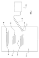
- Figure 1 illustrates an item, in this case a sheet of paper 10, bearing printing 12, which has been annotated with electronic data using a plurality of memory tags 14.
- the memory tags 14 have been secured to the sheet of paper 10 at various locations over it's surface, although they may alternatively be embedded in the paper sheet 10, preferably in locations identified by the printing 12, in order to assist in locating them for the purposes of reading data from or writing data to the memory tags 14.
- a hand held read/write device 16 is used to communicate with the memory tags 14 in wireless manner, as will be discussed further below.
- the read/write device 16 is also connected to a host computer, display, data rendering device or other apparatus 18 from which the data for writing to the memory tags 14 is received, and/or the data read from the memory tags 14 is passed.
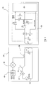
- the memory tag 14 is an RFID memory tag provided on a chip, and comprises an RFID transponder circuit 20, a memory 22, a power supply capacitor 24 and an antenna coil 26 having only a few turns e.g. five, or as in this case a single turn.
- the RFID transponder circuit 20 operates at 2.45GHz, is of an area of approximately 0.5 mm 2 , and will be described further below.
- the memory 22 provides IMbit of capacity of non-volatile memory and is of an area of approximately 1 mm 2 , and uses FRAM (ferroelectric random access memory) or MRAM (magnetoresistive random access memory) or similar memory technology requiring low power.
- the memory tags 14 are of a substantially square shape in plan view with an external dimension D for their sides of around 1 mm.
- the RFID transponder circuit 20 of the memory tag 14 comprises a capacitor C2 which, in combination with the antenna coil L2(26), forms a resonant circuit with component values being chosen to tune the combination to approximately 2.45GHz for inductive coupling with the read/write device 16.
- the portion of transponder circuit 20 responsible for power supply is diode D1 and capacitor C4(24), with diode D1 rectifying the alternating current generated by the inductive coupling and the capacitor C4 acts as a power supply storage.
- the portion of the transponder circuit 20 responsible for receiving transmitted data from the read/write device 16 is diode D2, capacitor C5 and resistor R1 which form a simple envelope detector; the data thus received is stored in memory 22.
- the portion of the transponder circuit 20 responsible for the reading of data from the memory 22 is the tuned circuit L2/C2 in combination with S1 and C3, switching C3 in and out of the circuit using S1 changes the resonance of tuned circuit L2/C2 resulting in phase modulation of the reflected power from the memory tag 14 to the read/write device 16.
- the circuit 28 of the read/write device 16 comprises a signal generator 30 which generates a signal at the chosen frequency of 2.45GHz. This signal passes via an amplitude modulator 32, where it is amplitude modulated with data to be written to the memory tag 14, and a splitter 34, to an antenna L1 and capacitor C1 which form a tuned circuit.
- the component values of L1 and C1 being chosen to tune it to 2.45GHz, as for the tuned circuit in the memory tag 14, in order to maximise inductive coupling between the two circuits, and thus transmission of power and data to the memory tag 14.
- the splitter 34 takes a part (as much as 50% of the power) of the amplitude modulated signal, for use as a reference signal, and passes it to a multiplier 36.
- the transmitted amplitude modulated signal and received signal are multiplied and then pass through a low pass filter 40 to provide a signal comprising the phase modulation from the memory tag 14 and thus indicative of the data read from the memory tag 14.
- This signal is then passed to the host computer or other device 18 to which the read/write device 16 is connected, for subsequent data processing.
- Amplitude Shift Keying (ASK) which only requires the simple envelope detector D2/C5 described in the circuit 20.
- ASK Amplitude Shift Keying
- FSK Frequency Shift Keying
- PSK Phase Shift Keying
- power transfer of around 25% can be achieved with a distance of around 1.8mm between the antennae L1 and L2, of the read/write device 16 and memory tag 14 respectively. This is sufficient to transfer enough power to the memory tag 14 for it to operate.
- the memory tags 14 have an external dimension D of around 1 mm, as described above, and therefore the read/write device 16 can communicate with them over a relatively short range, in this example of approximately 2D, (as illustrated on Figure 1 by broken circle 17).
- the distance over which the read/write device 16 and memory tag 14 will communicate effectively will clearly vary with the exact details of their construction, and it may therefore be up to 10D. Distances greater than this would limit the ability to use a plurality of memory tags 14 on a single sheet of paper 10, or other item, due to the distances which would be necessary between the memory tags 14 to ensure that the read/write device 16 does communicate with the desired memory tag 14 out of a number present.
- a communication distance of 5D or less is preferable.
- the memory tags 14 will preferably have a data rate of 10Mbitss -1 , which is two orders of magnitude faster than is typical in prior art devices. Such a data rate would enable the read/write device 16 to be held over the memory tag for a very short period of time ("brush and go") for the data to be read or written as appropriate.
- memory tags 14 described above operate at 2.45GHz it should be understood that memory tags operating at other frequencies may be used to implement the invention.
- Factors affacting the choice of operating frequency for the memory tags are: a) government regulations concerning radio frequency transmissions; b) adequate bandwidth (consistent with government regulations); c) frequency high enough to render the physical size of components in the memory tag small enough to keep the area of silicon required low (and hence the cost to manufacture low); d) frequency low enough to provide adequate performance when using low-cost high-volume CMOS technology to manufacture the memory tag.
Landscapes
- Engineering & Computer Science (AREA)
- Physics & Mathematics (AREA)
- General Physics & Mathematics (AREA)
- Theoretical Computer Science (AREA)
- Computer Hardware Design (AREA)
- Microelectronics & Electronic Packaging (AREA)
- Artificial Intelligence (AREA)
- Computer Networks & Wireless Communication (AREA)
- Computer Vision & Pattern Recognition (AREA)
- Health & Medical Sciences (AREA)
- Toxicology (AREA)
- General Health & Medical Sciences (AREA)
- Electromagnetism (AREA)
- Near-Field Transmission Systems (AREA)
- Radar Systems Or Details Thereof (AREA)
Applications Claiming Priority (2)
| Application Number | Priority Date | Filing Date | Title |
|---|---|---|---|
| GB0227197A GB2395592B (en) | 2002-11-21 | 2002-11-21 | Method of annotating an item with electronic data and apparatus therefor |
| GB0227197 | 2002-11-21 |
Publications (2)
| Publication Number | Publication Date |
|---|---|
| EP1422658A2 true EP1422658A2 (fr) | 2004-05-26 |
| EP1422658A3 EP1422658A3 (fr) | 2006-12-13 |
Family
ID=9948275
Family Applications (1)
| Application Number | Title | Priority Date | Filing Date |
|---|---|---|---|
| EP03257042A Ceased EP1422658A3 (fr) | 2002-11-21 | 2003-11-07 | Méthode et dispositif d'annotation d'un objet avec des données électroniques |
Country Status (3)
| Country | Link |
|---|---|
| US (2) | US7142115B2 (fr) |
| EP (1) | EP1422658A3 (fr) |
| GB (1) | GB2395592B (fr) |
Cited By (6)
| Publication number | Priority date | Publication date | Assignee | Title |
|---|---|---|---|---|
| GB2419780A (en) * | 2004-10-29 | 2006-05-03 | Hewlett Packard Development Co | Interaction between Service Providers and Customers |
| WO2009103293A1 (fr) * | 2008-02-18 | 2009-08-27 | Aalborg Universitet | Amélioration du rendement de puissance de la technique de modulation par déplacement de charge |
| EP2397976A3 (fr) * | 2007-10-02 | 2012-04-04 | Sharp Kabushiki Kaisha | Dispositif de stockage semi-conducteur et système de stockage |
| US8463663B2 (en) | 2004-10-29 | 2013-06-11 | Hewlett-Packard Development Company, L.P. | Storage of purchase-related information |
| US8970375B2 (en) | 2005-06-14 | 2015-03-03 | Hewlett-Packard Development Company, L.P. | Memory tag, method for providing information and enabling the release of stored content, and apparatus therefor |
| US9286613B2 (en) | 2004-10-29 | 2016-03-15 | Hewlett-Packard Development Company, L.P. | Ordering of goods or services using memory for storing digital content |
Families Citing this family (20)
| Publication number | Priority date | Publication date | Assignee | Title |
|---|---|---|---|---|
| US7487112B2 (en) | 2000-06-29 | 2009-02-03 | Barnes Jr Melvin L | System, method, and computer program product for providing location based services and mobile e-commerce |
| US8611919B2 (en) | 2002-05-23 | 2013-12-17 | Wounder Gmbh., Llc | System, method, and computer program product for providing location based services and mobile e-commerce |
| US10489449B2 (en) | 2002-05-23 | 2019-11-26 | Gula Consulting Limited Liability Company | Computer accepting voice input and/or generating audible output |
| GB2397272B (en) * | 2003-01-15 | 2006-11-15 | Hewlett Packard Co | Secure physical documents and methods and apparatus for publishing and reading them |
| GB2397273B (en) * | 2003-01-15 | 2007-08-01 | Hewlett Packard Co | Physial multimedia documents and methods and apparatus for publishing and reading them |
| GB2410590B (en) * | 2004-01-30 | 2007-02-14 | Hewlett Packard Development Co | Physical object with memory tag and apparatus for use with such objects |
| GB0402025D0 (en) * | 2004-01-30 | 2004-03-03 | Hewlett Packard Development Co | Physical object with memory tag and apparatus for use with such objects |
| US7246754B2 (en) * | 2004-02-18 | 2007-07-24 | Hewlett-Packard Development Company, L.P. | Secure currency |
| GB2418760B (en) * | 2004-10-01 | 2010-07-14 | Hewlett Packard Development Co | Securing electronic annotations |
| DE202004019107U1 (de) * | 2004-12-10 | 2006-04-20 | Wincor Nixdorf International Gmbh | Wettschein |
| JP4843249B2 (ja) * | 2005-05-10 | 2011-12-21 | 富士通株式会社 | タグ情報管理装置およびicタグ |
| GB2428122B (en) * | 2005-07-08 | 2011-03-23 | Hewlett Packard Development Co | Pharmaceutical product packaging |
| WO2007096793A1 (fr) * | 2006-02-22 | 2007-08-30 | Koninklijke Philips Electronics N.V. | Élément imprimé comportant une mémoire |
| DE102008027347A1 (de) * | 2008-06-07 | 2009-12-10 | Wincor Nixdorf International Gmbh | Verfahren und Vorrichtung zum Bearbeiten von Spielscheinen |
| US8151023B2 (en) * | 2008-08-26 | 2012-04-03 | Sandisk Il Ltd. | Hybrid storage of documents |
| US11783138B2 (en) * | 2012-04-04 | 2023-10-10 | Hypertherm, Inc. | Configuring signal devices in thermal processing systems |
| US12275082B2 (en) | 2013-11-13 | 2025-04-15 | Hypertherm, Inc. | Consumable cartridge for a plasma arc cutting system |
| US12521905B2 (en) | 2014-03-07 | 2026-01-13 | Hypertherm, Inc. | Liquid pressurization pump and systems with data storage |
| MX2019009420A (es) | 2017-02-09 | 2019-10-02 | Hypertherm Inc | Anillo rotacional y elemento de contacto para un cartucho de antorcha de arco de plasma. |
| CN108229617B (zh) * | 2018-01-15 | 2019-10-01 | 重庆品胜科技有限公司 | 标签打印机的rfid标签打印方法以及标签打印机 |
Family Cites Families (20)
| Publication number | Priority date | Publication date | Assignee | Title |
|---|---|---|---|---|
| US6097301A (en) * | 1996-04-04 | 2000-08-01 | Micron Communications, Inc. | RF identification system with restricted range |
| US5790946A (en) * | 1993-07-15 | 1998-08-04 | Rotzoll; Robert R. | Wake up device for a communications system |
| US5971281A (en) * | 1996-08-26 | 1999-10-26 | Storage Technology Corporation | Method for storing multiple logical data volumes on a single physical volume utilizing writable labels and physical volume produced thereby |
| US6164532A (en) * | 1997-05-15 | 2000-12-26 | Hitachi, Ltd. | Power transmission system, power transmission/communication system and reader and/or writer |
| US6104291A (en) * | 1998-01-09 | 2000-08-15 | Intermec Ip Corp. | Method and apparatus for testing RFID tags |
| US6362738B1 (en) * | 1998-04-16 | 2002-03-26 | Motorola, Inc. | Reader for use in a radio frequency identification system and method thereof |
| US20030225572A1 (en) * | 1998-07-08 | 2003-12-04 | Adams Guy De Warrenne Bruce | Selectively attachable device for electronic annotation and methods therefor |
| US6342830B1 (en) * | 1998-09-10 | 2002-01-29 | Xerox Corporation | Controlled shielding of electronic tags |
| US6446208B1 (en) * | 1998-09-10 | 2002-09-03 | Xerox Corporation | User interface system based on sequentially read electronic tags |
| JP4144954B2 (ja) * | 1999-01-08 | 2008-09-03 | 横浜ゴム株式会社 | タイヤ用トランスポンダのスキャナ |
| US6246326B1 (en) * | 1999-05-05 | 2001-06-12 | Intermec Ip Corp. | Performance optimized smart label printer |
| JP2001024145A (ja) * | 1999-07-13 | 2001-01-26 | Shinko Electric Ind Co Ltd | 半導体装置及びその製造方法 |
| US6259369B1 (en) * | 1999-09-30 | 2001-07-10 | Moore North America, Inc. | Low cost long distance RFID reading |
| TW531976B (en) * | 2001-01-11 | 2003-05-11 | Hanex Co Ltd | Communication apparatus and installing structure, manufacturing method and communication method |
| DE10159395B4 (de) * | 2001-12-04 | 2010-11-11 | Braun Gmbh | Vorrichtung zur Zahnreinigung |
| GB2397273B (en) * | 2003-01-15 | 2007-08-01 | Hewlett Packard Co | Physial multimedia documents and methods and apparatus for publishing and reading them |
| GB2397272B (en) * | 2003-01-15 | 2006-11-15 | Hewlett Packard Co | Secure physical documents and methods and apparatus for publishing and reading them |
| US8025573B2 (en) * | 2004-07-30 | 2011-09-27 | Hewlett-Packard Development Company, L.P. | Physical representational objects with digital memory and methods of manufacture and use thereof |
| GB2416893A (en) * | 2004-07-30 | 2006-02-08 | Hewlett Packard Development Co | Providing digital rewards associated with physical products |
| GB2422692B (en) * | 2005-01-31 | 2009-08-12 | Hewlett Packard Development Co | Software updates for electronic appliances |
-
2002
- 2002-11-21 GB GB0227197A patent/GB2395592B/en not_active Expired - Fee Related
-
2003
- 2003-10-31 US US10/697,265 patent/US7142115B2/en not_active Expired - Lifetime
- 2003-11-07 EP EP03257042A patent/EP1422658A3/fr not_active Ceased
-
2006
- 2006-11-22 US US11/708,740 patent/US7535359B2/en not_active Expired - Fee Related
Cited By (7)
| Publication number | Priority date | Publication date | Assignee | Title |
|---|---|---|---|---|
| GB2419780A (en) * | 2004-10-29 | 2006-05-03 | Hewlett Packard Development Co | Interaction between Service Providers and Customers |
| US8463663B2 (en) | 2004-10-29 | 2013-06-11 | Hewlett-Packard Development Company, L.P. | Storage of purchase-related information |
| US9286613B2 (en) | 2004-10-29 | 2016-03-15 | Hewlett-Packard Development Company, L.P. | Ordering of goods or services using memory for storing digital content |
| US8970375B2 (en) | 2005-06-14 | 2015-03-03 | Hewlett-Packard Development Company, L.P. | Memory tag, method for providing information and enabling the release of stored content, and apparatus therefor |
| EP2397976A3 (fr) * | 2007-10-02 | 2012-04-04 | Sharp Kabushiki Kaisha | Dispositif de stockage semi-conducteur et système de stockage |
| US8655350B2 (en) | 2007-10-02 | 2014-02-18 | Sharp Kabushiki Kaisha | Semiconductor storage device and storage system |
| WO2009103293A1 (fr) * | 2008-02-18 | 2009-08-27 | Aalborg Universitet | Amélioration du rendement de puissance de la technique de modulation par déplacement de charge |
Also Published As
| Publication number | Publication date |
|---|---|
| US20040099743A1 (en) | 2004-05-27 |
| GB2395592B (en) | 2006-05-17 |
| EP1422658A3 (fr) | 2006-12-13 |
| US7535359B2 (en) | 2009-05-19 |
| GB2395592A (en) | 2004-05-26 |
| US7142115B2 (en) | 2006-11-28 |
| GB0227197D0 (en) | 2002-12-24 |
| US20070164864A1 (en) | 2007-07-19 |
Similar Documents
| Publication | Publication Date | Title |
|---|---|---|
| US7142115B2 (en) | Method of annotating an item with electronic data and apparatus therefor | |
| US7855646B2 (en) | Inductive coupling in documents | |
| US11288565B2 (en) | Non-transferable radio frequency identification label or tag | |
| AU2003220174B2 (en) | Integrated circuit with enhanced coupling | |
| US9098790B2 (en) | Methods and apparatus for preserving privacy in an RFID system | |
| JP2009537886A (ja) | 複数のアンテナ及びそれに付随するアンテナ選択回路を有する非接触型無線周波数デバイス | |
| CN101542499B (zh) | 借助于无源谐振电路的射频通信应答器的优化读取方法和系统 | |
| JP3649374B2 (ja) | アンテナ装置及びカード状記憶媒体 | |
| GB2412153A (en) | Digital pen with a memory tag reader/writer | |
| US8441340B2 (en) | Tag communication devices | |
| US7362625B2 (en) | Interface configuration by a memory tag | |
| KR101388156B1 (ko) | 반도체장치 | |
| GB2423673A (en) | Memory tag attached to document storing revision information | |
| JP5427345B2 (ja) | Rfid用icチップ | |
| JP2006185373A (ja) | 非接触認識装置を備えた積層シート状製品および通信方法 | |
| JP2001005926A (ja) | 非接触情報媒体及びこれを用いた通信システム | |
| HK1136099A (en) | Device with no radiofrequency contact comprising several antennas and associated antenna selection circuit | |
| JP2015225577A (ja) | 電子パスポート | |
| JP2007258924A (ja) | 無線タグ用アンテナ及びこれを使用した物品の管理システム |
Legal Events
| Date | Code | Title | Description |
|---|---|---|---|
| PUAI | Public reference made under article 153(3) epc to a published international application that has entered the european phase |
Free format text: ORIGINAL CODE: 0009012 |
|
| AK | Designated contracting states |
Kind code of ref document: A2 Designated state(s): AT BE BG CH CY CZ DE DK EE ES FI FR GB GR HU IE IT LI LU MC NL PT RO SE SI SK TR |
|
| AX | Request for extension of the european patent |
Extension state: AL LT LV MK |
|
| PUAL | Search report despatched |
Free format text: ORIGINAL CODE: 0009013 |
|
| AK | Designated contracting states |
Kind code of ref document: A3 Designated state(s): AT BE BG CH CY CZ DE DK EE ES FI FR GB GR HU IE IT LI LU MC NL PT RO SE SI SK TR |
|
| AX | Request for extension of the european patent |
Extension state: AL LT LV MK |
|
| 17P | Request for examination filed |
Effective date: 20070530 |
|
| 17Q | First examination report despatched |
Effective date: 20070703 |
|
| AKX | Designation fees paid |
Designated state(s): AT BE BG CH CY CZ DE DK EE ES FI FR GB GR HU IE IT LI LU MC NL PT RO SE SI SK TR |
|
| STAA | Information on the status of an ep patent application or granted ep patent |
Free format text: STATUS: THE APPLICATION HAS BEEN REFUSED |
|
| 18R | Application refused |
Effective date: 20081010 |