EP1422748A1 - Film semi-conducteur en nitrure du groupe iii et son procede de production - Google Patents
Film semi-conducteur en nitrure du groupe iii et son procede de production Download PDFInfo
- Publication number
- EP1422748A1 EP1422748A1 EP02751808A EP02751808A EP1422748A1 EP 1422748 A1 EP1422748 A1 EP 1422748A1 EP 02751808 A EP02751808 A EP 02751808A EP 02751808 A EP02751808 A EP 02751808A EP 1422748 A1 EP1422748 A1 EP 1422748A1
- Authority
- EP
- European Patent Office
- Prior art keywords
- group iii
- nitride semiconductor
- iii nitride
- nano
- etching
- Prior art date
- Legal status (The legal status is an assumption and is not a legal conclusion. Google has not performed a legal analysis and makes no representation as to the accuracy of the status listed.)
- Withdrawn
Links
Images



Classifications
-
- C—CHEMISTRY; METALLURGY
- C30—CRYSTAL GROWTH
- C30B—SINGLE-CRYSTAL GROWTH; UNIDIRECTIONAL SOLIDIFICATION OF EUTECTIC MATERIAL OR UNIDIRECTIONAL DEMIXING OF EUTECTOID MATERIAL; REFINING BY ZONE-MELTING OF MATERIAL; PRODUCTION OF A HOMOGENEOUS POLYCRYSTALLINE MATERIAL WITH DEFINED STRUCTURE; SINGLE CRYSTALS OR HOMOGENEOUS POLYCRYSTALLINE MATERIAL WITH DEFINED STRUCTURE; AFTER-TREATMENT OF SINGLE CRYSTALS OR A HOMOGENEOUS POLYCRYSTALLINE MATERIAL WITH DEFINED STRUCTURE; APPARATUS THEREFOR
- C30B25/00—Single-crystal growth by chemical reaction of reactive gases, e.g. chemical vapour-deposition growth
- C30B25/02—Epitaxial-layer growth
-
- C—CHEMISTRY; METALLURGY
- C30—CRYSTAL GROWTH
- C30B—SINGLE-CRYSTAL GROWTH; UNIDIRECTIONAL SOLIDIFICATION OF EUTECTIC MATERIAL OR UNIDIRECTIONAL DEMIXING OF EUTECTOID MATERIAL; REFINING BY ZONE-MELTING OF MATERIAL; PRODUCTION OF A HOMOGENEOUS POLYCRYSTALLINE MATERIAL WITH DEFINED STRUCTURE; SINGLE CRYSTALS OR HOMOGENEOUS POLYCRYSTALLINE MATERIAL WITH DEFINED STRUCTURE; AFTER-TREATMENT OF SINGLE CRYSTALS OR A HOMOGENEOUS POLYCRYSTALLINE MATERIAL WITH DEFINED STRUCTURE; APPARATUS THEREFOR
- C30B29/00—Single crystals or homogeneous polycrystalline material with defined structure characterised by the material or by their shape
- C30B29/10—Inorganic compounds or compositions
- C30B29/40—AIIIBV compounds wherein A is B, Al, Ga, In or Tl and B is N, P, As, Sb or Bi
- C30B29/403—AIII-nitrides
-
- C—CHEMISTRY; METALLURGY
- C30—CRYSTAL GROWTH
- C30B—SINGLE-CRYSTAL GROWTH; UNIDIRECTIONAL SOLIDIFICATION OF EUTECTIC MATERIAL OR UNIDIRECTIONAL DEMIXING OF EUTECTOID MATERIAL; REFINING BY ZONE-MELTING OF MATERIAL; PRODUCTION OF A HOMOGENEOUS POLYCRYSTALLINE MATERIAL WITH DEFINED STRUCTURE; SINGLE CRYSTALS OR HOMOGENEOUS POLYCRYSTALLINE MATERIAL WITH DEFINED STRUCTURE; AFTER-TREATMENT OF SINGLE CRYSTALS OR A HOMOGENEOUS POLYCRYSTALLINE MATERIAL WITH DEFINED STRUCTURE; APPARATUS THEREFOR
- C30B29/00—Single crystals or homogeneous polycrystalline material with defined structure characterised by the material or by their shape
- C30B29/10—Inorganic compounds or compositions
- C30B29/40—AIIIBV compounds wherein A is B, Al, Ga, In or Tl and B is N, P, As, Sb or Bi
- C30B29/403—AIII-nitrides
- C30B29/406—Gallium nitride
-
- C—CHEMISTRY; METALLURGY
- C30—CRYSTAL GROWTH
- C30B—SINGLE-CRYSTAL GROWTH; UNIDIRECTIONAL SOLIDIFICATION OF EUTECTIC MATERIAL OR UNIDIRECTIONAL DEMIXING OF EUTECTOID MATERIAL; REFINING BY ZONE-MELTING OF MATERIAL; PRODUCTION OF A HOMOGENEOUS POLYCRYSTALLINE MATERIAL WITH DEFINED STRUCTURE; SINGLE CRYSTALS OR HOMOGENEOUS POLYCRYSTALLINE MATERIAL WITH DEFINED STRUCTURE; AFTER-TREATMENT OF SINGLE CRYSTALS OR A HOMOGENEOUS POLYCRYSTALLINE MATERIAL WITH DEFINED STRUCTURE; APPARATUS THEREFOR
- C30B29/00—Single crystals or homogeneous polycrystalline material with defined structure characterised by the material or by their shape
- C30B29/60—Single crystals or homogeneous polycrystalline material with defined structure characterised by the material or by their shape characterised by shape
- C30B29/605—Products containing multiple oriented crystallites, e.g. columnar crystallites
-
- H—ELECTRICITY
- H10—SEMICONDUCTOR DEVICES; ELECTRIC SOLID-STATE DEVICES NOT OTHERWISE PROVIDED FOR
- H10H—INORGANIC LIGHT-EMITTING SEMICONDUCTOR DEVICES HAVING POTENTIAL BARRIERS
- H10H20/00—Individual inorganic light-emitting semiconductor devices having potential barriers, e.g. light-emitting diodes [LED]
- H10H20/80—Constructional details
- H10H20/81—Bodies
- H10H20/819—Bodies characterised by their shape, e.g. curved or truncated substrates
- H10H20/82—Roughened surfaces, e.g. at the interface between epitaxial layers
-
- H—ELECTRICITY
- H10—SEMICONDUCTOR DEVICES; ELECTRIC SOLID-STATE DEVICES NOT OTHERWISE PROVIDED FOR
- H10P—GENERIC PROCESSES OR APPARATUS FOR THE MANUFACTURE OR TREATMENT OF DEVICES COVERED BY CLASS H10
- H10P14/00—Formation of materials, e.g. in the shape of layers or pillars
- H10P14/20—Formation of materials, e.g. in the shape of layers or pillars of semiconductor materials
- H10P14/27—Formation of materials, e.g. in the shape of layers or pillars of semiconductor materials using selective deposition, e.g. simultaneous growth of monocrystalline and non-monocrystalline semiconductor materials
- H10P14/271—Formation of materials, e.g. in the shape of layers or pillars of semiconductor materials using selective deposition, e.g. simultaneous growth of monocrystalline and non-monocrystalline semiconductor materials characterised by the preparation of substrate for selective deposition
-
- H—ELECTRICITY
- H10—SEMICONDUCTOR DEVICES; ELECTRIC SOLID-STATE DEVICES NOT OTHERWISE PROVIDED FOR
- H10P—GENERIC PROCESSES OR APPARATUS FOR THE MANUFACTURE OR TREATMENT OF DEVICES COVERED BY CLASS H10
- H10P14/00—Formation of materials, e.g. in the shape of layers or pillars
- H10P14/20—Formation of materials, e.g. in the shape of layers or pillars of semiconductor materials
- H10P14/27—Formation of materials, e.g. in the shape of layers or pillars of semiconductor materials using selective deposition, e.g. simultaneous growth of monocrystalline and non-monocrystalline semiconductor materials
- H10P14/276—Lateral overgrowth
- H10P14/278—Pendeoepitaxy
-
- H—ELECTRICITY
- H10—SEMICONDUCTOR DEVICES; ELECTRIC SOLID-STATE DEVICES NOT OTHERWISE PROVIDED FOR
- H10P—GENERIC PROCESSES OR APPARATUS FOR THE MANUFACTURE OR TREATMENT OF DEVICES COVERED BY CLASS H10
- H10P14/00—Formation of materials, e.g. in the shape of layers or pillars
- H10P14/20—Formation of materials, e.g. in the shape of layers or pillars of semiconductor materials
- H10P14/29—Formation of materials, e.g. in the shape of layers or pillars of semiconductor materials characterised by the substrates
- H10P14/2901—Materials
- H10P14/2921—Materials being crystalline insulating materials
-
- H—ELECTRICITY
- H10—SEMICONDUCTOR DEVICES; ELECTRIC SOLID-STATE DEVICES NOT OTHERWISE PROVIDED FOR
- H10P—GENERIC PROCESSES OR APPARATUS FOR THE MANUFACTURE OR TREATMENT OF DEVICES COVERED BY CLASS H10
- H10P14/00—Formation of materials, e.g. in the shape of layers or pillars
- H10P14/20—Formation of materials, e.g. in the shape of layers or pillars of semiconductor materials
- H10P14/32—Formation of materials, e.g. in the shape of layers or pillars of semiconductor materials characterised by intermediate layers between substrates and deposited layers
- H10P14/3202—Materials thereof
- H10P14/3214—Materials thereof being Group IIIA-VA semiconductors
- H10P14/3216—Nitrides
-
- H—ELECTRICITY
- H10—SEMICONDUCTOR DEVICES; ELECTRIC SOLID-STATE DEVICES NOT OTHERWISE PROVIDED FOR
- H10P—GENERIC PROCESSES OR APPARATUS FOR THE MANUFACTURE OR TREATMENT OF DEVICES COVERED BY CLASS H10
- H10P14/00—Formation of materials, e.g. in the shape of layers or pillars
- H10P14/20—Formation of materials, e.g. in the shape of layers or pillars of semiconductor materials
- H10P14/32—Formation of materials, e.g. in the shape of layers or pillars of semiconductor materials characterised by intermediate layers between substrates and deposited layers
- H10P14/3242—Structure
- H10P14/3244—Layer structure
- H10P14/3248—Layer structure consisting of two layers
-
- H—ELECTRICITY
- H10—SEMICONDUCTOR DEVICES; ELECTRIC SOLID-STATE DEVICES NOT OTHERWISE PROVIDED FOR
- H10P—GENERIC PROCESSES OR APPARATUS FOR THE MANUFACTURE OR TREATMENT OF DEVICES COVERED BY CLASS H10
- H10P14/00—Formation of materials, e.g. in the shape of layers or pillars
- H10P14/20—Formation of materials, e.g. in the shape of layers or pillars of semiconductor materials
- H10P14/32—Formation of materials, e.g. in the shape of layers or pillars of semiconductor materials characterised by intermediate layers between substrates and deposited layers
- H10P14/3242—Structure
- H10P14/3256—Microstructure
-
- H—ELECTRICITY
- H10—SEMICONDUCTOR DEVICES; ELECTRIC SOLID-STATE DEVICES NOT OTHERWISE PROVIDED FOR
- H10P—GENERIC PROCESSES OR APPARATUS FOR THE MANUFACTURE OR TREATMENT OF DEVICES COVERED BY CLASS H10
- H10P14/00—Formation of materials, e.g. in the shape of layers or pillars
- H10P14/20—Formation of materials, e.g. in the shape of layers or pillars of semiconductor materials
- H10P14/34—Deposited materials, e.g. layers
- H10P14/3402—Deposited materials, e.g. layers characterised by the chemical composition
- H10P14/3414—Deposited materials, e.g. layers characterised by the chemical composition being group IIIA-VIA materials
- H10P14/3416—Nitrides
-
- H—ELECTRICITY
- H10—SEMICONDUCTOR DEVICES; ELECTRIC SOLID-STATE DEVICES NOT OTHERWISE PROVIDED FOR
- H10P—GENERIC PROCESSES OR APPARATUS FOR THE MANUFACTURE OR TREATMENT OF DEVICES COVERED BY CLASS H10
- H10P50/00—Etching of wafers, substrates or parts of devices
- H10P50/20—Dry etching; Plasma etching; Reactive-ion etching
- H10P50/24—Dry etching; Plasma etching; Reactive-ion etching of semiconductor materials
- H10P50/246—Dry etching; Plasma etching; Reactive-ion etching of semiconductor materials of Group III-V materials
-
- H—ELECTRICITY
- H10—SEMICONDUCTOR DEVICES; ELECTRIC SOLID-STATE DEVICES NOT OTHERWISE PROVIDED FOR
- H10P—GENERIC PROCESSES OR APPARATUS FOR THE MANUFACTURE OR TREATMENT OF DEVICES COVERED BY CLASS H10
- H10P50/00—Etching of wafers, substrates or parts of devices
- H10P50/69—Etching of wafers, substrates or parts of devices using masks for semiconductor materials
- H10P50/691—Etching of wafers, substrates or parts of devices using masks for semiconductor materials for Group V materials or Group III-V materials
- H10P50/693—Etching of wafers, substrates or parts of devices using masks for semiconductor materials for Group V materials or Group III-V materials characterised by their size, orientation, disposition, behaviour or shape, in horizontal or vertical plane
- H10P50/694—Etching of wafers, substrates or parts of devices using masks for semiconductor materials for Group V materials or Group III-V materials characterised by their size, orientation, disposition, behaviour or shape, in horizontal or vertical plane characterised by their behaviour during the process, e.g. soluble masks or redeposited masks
-
- H—ELECTRICITY
- H10—SEMICONDUCTOR DEVICES; ELECTRIC SOLID-STATE DEVICES NOT OTHERWISE PROVIDED FOR
- H10H—INORGANIC LIGHT-EMITTING SEMICONDUCTOR DEVICES HAVING POTENTIAL BARRIERS
- H10H20/00—Individual inorganic light-emitting semiconductor devices having potential barriers, e.g. light-emitting diodes [LED]
- H10H20/80—Constructional details
- H10H20/81—Bodies
- H10H20/822—Materials of the light-emitting regions
- H10H20/824—Materials of the light-emitting regions comprising only Group III-V materials, e.g. GaP
- H10H20/825—Materials of the light-emitting regions comprising only Group III-V materials, e.g. GaP containing nitrogen, e.g. GaN
-
- H—ELECTRICITY
- H10—SEMICONDUCTOR DEVICES; ELECTRIC SOLID-STATE DEVICES NOT OTHERWISE PROVIDED FOR
- H10P—GENERIC PROCESSES OR APPARATUS FOR THE MANUFACTURE OR TREATMENT OF DEVICES COVERED BY CLASS H10
- H10P14/00—Formation of materials, e.g. in the shape of layers or pillars
- H10P14/20—Formation of materials, e.g. in the shape of layers or pillars of semiconductor materials
- H10P14/24—Formation of materials, e.g. in the shape of layers or pillars of semiconductor materials using chemical vapour deposition [CVD]
Definitions
- the present invention relates to a group III nitride semiconductor film and a method of fabricating the same.
- a group III nitride semiconductor film for example, a mixed crystal Al x Ga y In 1-x-y N (0 ⁇ x ⁇ 1, 0 ⁇ y ⁇ 1 and 0 ⁇ x+y ⁇ 1) made by mixing GaN, Al or In at a suitable ratio has an energy gap ranging from 0.75 eV to 6.288 eV and is a direct transition type semiconductor. Accordingly, the group III nitride semiconductor has eminent characteristics in a luminous efficiency as compared with materials belonging to an indirect transition type such as SiC and is suitable for a material for light emitting diodes, laser diodes, ultraviolet ray detecting elements and the like.
- a buffer layer of AlN or GaN is formed on a substrate differing from the group III nitride semiconductor film in a lattice constant and a thermal expansion coefficient, such as sapphire, SiC, Si or GaAs.
- GaN is formed on the buffer layer by an epitaxial growth method.
- a known light-emitting chip of blue LED employing GaN has a double heterostructure in which a GaN buffer layer, n-type GaN layer, n-type GaAlN layer, InGaN layer, p-type GaAlN layer and p-type GaN layer are sequentially laminated on a sapphire substrate.
- a GaN film has a large number of lattice defects due to a difference in the lattice constant between a grown GaN film and the substrate. Accordingly, in order that a group III nitride semiconductor film having fewer lattice defects and a large film thickness may be made, an epitaxial lateral overgrowth (ELO) using a stripe mask (for example, JP-A-10-312971) or re-growth after partial elimination by etching (PENDEO) is carried out in order that a group III nitride semiconductor film having fewer lattice defects and a large film thickness may be made.
- ELO epitaxial lateral overgrowth
- PENDEO re-growth after partial elimination by etching
- ELO and PENDEO have been devised to make a GaN film with fewer lattice defects.
- spaces between growth starting parts are in the order of micrometers and relatively larger. Accordingly, the film is grown while lattice defects are transferred from lower layers to upper ones, whereupon a uniform crystal film involving fewer lattice defects cannot be obtained.
- a high purity group III nitride semiconductor film cannot be obtained in ELO by the influence of contamination by SiO 2 which is a mask material.
- no electrode can be provided on an upper side of the sapphire substrate since sapphire serving as the substrate material is electrically insulating. Accordingly, a part of the semiconductor film needs to be exposed in order that electrodes may be provided on the group III nitride semiconductor film.
- the group III nitride semiconductor film For example, when the foregoing double hetero structure is exemplified, parts of the p-type GaN layer which is an uppermost layer, p-type GaAlN layer, InGaN layer and n-type GaAlN layer are eliminated in this order.
- An n-electrode is provided on the surface of the n-type GaN layer.
- a p-electrode is provided on the surface of the uppermost p-type GaN layer.
- GaN has a larger refractive index than glass or the like (for example, glass has a refractive index of 1.5 and GaN 2.5) and accordingly, reflection on an interface between crystal and space results in a problem. More specifically, when GaN is used, the aforesaid problem is a loss in emitted light in a light-emitting element and a reduction in light detecting sensitivity in a light detecting element. Thus, the aforesaid problem is an obstacle to making full use of each element's performance, whereupon it is difficult to manufacture a light-emitting element or light detecting element each having superior characteristics. Processes as multilayer film coating have conventionally been employed to overcome the problem.
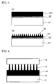
- a first invention is a method of fabricating a group III nitride semiconductor film characterized by 1 ⁇ a nano-pillar fabricating step of fabricating nano-pillars by dry-etching a group III nitride semiconductor film while an etching retarding substance having a smaller etching rate than the group III nitride semiconductor is present on a surface of the group III nitride semiconductor (a lower layer) to be etched, and 2 ⁇ a depositing step of depositing another group III nitride semiconductor (an upper layer) on the nano-pillars, thereby making the group III nitride semiconductor film.
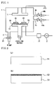
- the etching retarding substance is placed as a solid substance in an etching chamber in the 1 ⁇ nano-pillar fabricating step so as to be exposed to an etching gas in dry etching.
- the etching retarding substance is SiO 2 .
- a third invention is a methodof fabricating a group III nitride semiconductor film,characterized by 3 ⁇ anano-pillarfabricating step of dry-etching a group III nitride semiconductor film while an etching retarding substance having a smaller etching rate than the group III nitride semiconductor film is present on a surface of the group III nitride semiconductor film, thereby fabricating nano-pillars.
- a material for the group III nitride semiconductor film fabricated by the present invention is a group III-V semiconductor containing a group III element such as GaN, GaAlN, InGaN or the like (gallium, for example) and can generally be represented by chemical formula, Al x Ga y In 1-x-y N (0 ⁇ x ⁇ 1, 0 ⁇ y ⁇ 1 and 0 ⁇ x+y ⁇ 1).
- group III nitride semiconductor films may be pure or doped with impurity, which may be a p-type or n-type.
- the group III nitride semiconductor film may have a monolayer or multilayer structure.
- all the layers may be formed of the group III nitride semiconductor film or at least one of the layers may be formed of the group III nitride semiconductor film.
- the group III nitride semiconductor film may be formed on a substrate of sapphire or the like, for example.
- the present invention may be employed for fabrication of a group III nitride semiconductor film having a multilayer structure such as a double heterostructure, for example.
- dry etching is an etching method making use of gas discharge, differing from a chemical wet etching and includes for example, a reactive ion etching (RIE) , an electron cyclotron resonance etching (ECR) and an inductive coupling plasma etching (ICP).
- RIE reactive ion etching
- ECR electron cyclotron resonance etching
- ICP inductive coupling plasma etching
- the “nano-pillars” means a structure in which a plurality of small pillars each having a section sized in the nanometer order protrude.
- the nano-pillars have an exceedingly small probability of lattice defects which are present on the etched group III nitride semiconductor film.
- the aforesaid lattice defects even if the nano-pillars involve them, do not almost affect another group III nitride semiconductor film deposited with the top of each nano-pillar serving as a core of crystal growth.
- the light reflectance is reduced by providing nano-pillars on the surface of the group III nitride semiconductor film, whereby the light transmittance is improved.
- the dry-etching is carried out while the etching retarding substance is present on the surface of the target group III nitride semiconductor. Since the etching retarding substance has a lower etching rate than the group III nitride semiconductor, the etching retarding substance serves as a micro-mask on a part of the surface to which the etching retarding substance is adherent, so that a micro rugged structure is formed at an initial stage of the etching.
- the subsequently ionized etching retarding substance will adhere to the convex portion with higher probability.
- re-adherence of the etching retarding substance and etching by an etching gas plasma repeatedly progress, whereby the nano-pillars are fabricated.
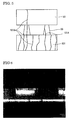
- nano-pillars have a dimension of not more than about 100 nm and in addition, a space (gap) between adjacent nano-pillars can be ranged from several tens nm to about 100 nm on the average. Accordingly, the nano-pillar and the gap can repeatedly be constructed at a distance of about 100 nm. Then, nano-pillars whose maximum number is about 1 ⁇ 10 6 are constructed for every 1 cm, and accordingly, nano-pillars whose maximum number is about 1 ⁇ 10 12 can be fabricated for every 1 cm 2 .
- a type of the etching gas is not dependent but any type of gas which can generally be used in the dry etching of the group III nitride semiconductor may be employed.
- an inert gas such as a Cl 2 gas, BCl 3 gas, SiCl 4 gas, SF 6 gas CHF 3 gas, CF 4 gas, CCl 2 F 2 gas, CCl 4 gas, Ar or the like may be employed individually or in a mixture.
- a flow rate of gas ranges from 0.1 ml/min to 500 ml/min.
- an internal pressure of the etching chamber in the dry etching is similar to that in the normal dry etching and can be set in a range from 0.01 Pa to 100 Pa, for example.
- a high frequency power density is the same as in the normal dry etching.
- an electric power density can be set to range from 0.01 W/cm 2 to 10 W/cm 2 .
- silicon dioxide SiO 2
- another group III nitride semiconductor (an upper layer) is deposited on the nano-pillars which serves as cores comprising thus formed group III nitride semiconductor (a lower layer) (2 ⁇ a depositing step).
- a chemical etching is carried out in order that the etching retarding substance on the nano-pillar surfaces may be eliminated completely so that the elimination contributes to smooth formation of the upper layer.
- a method of depositing the upper layer is exemplified a metal organic vapor phase epitaxy method (MOVPE), a hydride VPE method (HVPE), a molecular beam epitaxy method (MBE) or the like.
- the probability that lattice defects present in the lower layer group III nitride semiconductor remains present in the nano-pillars is exceedingly small. Accordingly, the group III nitride semiconductor (an upper layer) involving fewer lattice defects is deposited on an upper face of the lower layer.
- the upper layer is deposited on the nano-pillars comprising the group III nitride semiconductor having the same physical properties such as the lattice constant as the upper layer. Accordingly, the upper layer is exceedingly stable as compared with the case where the upper layer is deposited on an upper face of the substance having a different lattice constant and thermal expansion coefficient such as sapphire as in the conventional structure.
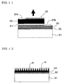
- a method of separating the nano-pillars from the upper layer includes physical methods (for example, cutting by a sharp blade or a cutter provided with a substance having a high hardness, such as diamond or breaking the nano-pillars by application of impulse or shearing stress) and chemical methods (melting only the nano-pillars by soaking them in an etchant, thereby separating the nano-pillars). Furthermore, it is preferable that the face on which the nano-pillars are located is ground and flattened.
- optical devices such as light emitting elements, bipolar devices such as transistors and unipolar devices such as FET's can be fabricated.
- the group III nitride semiconductor film having no stress-strain, fewer lattice defects and a large thickness can efficiently be fabricated in a short period of time. Furthermore, the mixed crystal involving fewer lattice defects, Al x Ga y In 1-x-y N (0 ⁇ x ⁇ 1, 0 ⁇ y ⁇ 1 and 0 ⁇ x+y ⁇ 1), is formed on the aforesaid group III nitride semiconductor film, whereby a multilayer film can be formed. Consequently, light emitting and detecting devices having high light emitting and detecting efficiencies respectively can be provided.
- Nano-pillars 50 are thus formed on the surface of the group III nitride semiconductor film 101 by the etching, as shown in FIG. 8D.
- Each nano-pillar 50 has a diameter ranging from about 10 nm to about 200 nm.
- a space between each nano-pillar 50 and another nano-pillar 50 adjacent thereto is about 100 nm on the average.
- the diameter and space of the nano-pillars 50 can be changed suitably according the conditions of the etching.
- a mask in the order of nanometer is required when an ordinary lithography is used for formation of the above-described nano-pillars.
- a wavelength in the order of nanometer is also necessary for light used in the exposure. Consequently, a method using the lithography cannot currently be realized.
- a pair of positive and negative electrodes 57A and 57B are formed on the group III nitride semiconductor film thus fabricated.
- the positive electrode 57A is formed on the upper side of the p-GaN layer 62.
- the negative electrode 57B is formed on the surface of the n-GaN layer 60 after a depression has been formed by the etching so as to extend through the p-GaN layer 62 and InGaN layer 61 and reach the n-GaN layer 60.
- SiO 2 was deposited on the upper side of GaN, for example, by the RF sputtering, so as to have a thickness of about 300 nm and a line of 5 ⁇ m wide and space pattern were fabricated in the ⁇ 1100> direction by the ordinary photolithography technique, whereby an etching sample 55 was made.
- GaN an upper layer
- TMG trimethyl gallium
- NH 3 was caused to flow at ⁇ mol/min.
- the temperature was 1000°C and pressure was 300 Torr. Under these conditions, the growth of GaN by about 3 ⁇ m to 4 ⁇ m per hour was confirmed.
- GaN of the upper layer had a film thickness of about 3 ⁇ m.
Landscapes
- Chemical & Material Sciences (AREA)
- Engineering & Computer Science (AREA)
- Crystallography & Structural Chemistry (AREA)
- Materials Engineering (AREA)
- Metallurgy (AREA)
- Organic Chemistry (AREA)
- Inorganic Chemistry (AREA)
- Chemical Kinetics & Catalysis (AREA)
- General Chemical & Material Sciences (AREA)
- Led Devices (AREA)
- Drying Of Semiconductors (AREA)
- Recrystallisation Techniques (AREA)
Applications Claiming Priority (3)
| Application Number | Priority Date | Filing Date | Title |
|---|---|---|---|
| JP2001233011 | 2001-08-01 | ||
| JP2001233011 | 2001-08-01 | ||
| PCT/JP2002/007748 WO2003015143A1 (fr) | 2001-08-01 | 2002-07-30 | Film semi-conducteur en nitrure du groupe iii et son procede de production |
Publications (1)
| Publication Number | Publication Date |
|---|---|
| EP1422748A1 true EP1422748A1 (fr) | 2004-05-26 |
Family
ID=19064839
Family Applications (1)
| Application Number | Title | Priority Date | Filing Date |
|---|---|---|---|
| EP02751808A Withdrawn EP1422748A1 (fr) | 2001-08-01 | 2002-07-30 | Film semi-conducteur en nitrure du groupe iii et son procede de production |
Country Status (4)
| Country | Link |
|---|---|
| US (1) | US20040157358A1 (fr) |
| EP (1) | EP1422748A1 (fr) |
| JP (1) | JPWO2003015143A1 (fr) |
| WO (1) | WO2003015143A1 (fr) |
Cited By (15)
| Publication number | Priority date | Publication date | Assignee | Title |
|---|---|---|---|---|
| WO2006035212A1 (fr) * | 2004-09-28 | 2006-04-06 | Wang Nang Wang | Diodes electroluminescentes texturees |
| WO2007107757A3 (fr) * | 2006-03-23 | 2007-11-15 | Univ Bath | Procédé de tirage au moyen de couches conformes et de hvpe pour la production de matériaux semi-conducteurs composés de haute qualité |
| WO2008087452A1 (fr) * | 2007-01-19 | 2008-07-24 | Nanogan Limited | Production de matériau semiconducteur monocristallin au moyen d'un modèle de nanostructure |
| EP1727217A3 (fr) * | 2005-05-24 | 2009-03-11 | LG Electronics, Inc. | Dispositif lumineux à nanostructures pour extraction de lumière |
| WO2009040580A1 (fr) * | 2007-09-26 | 2009-04-02 | Wang Nang Wang | Semiconducteur au nitrure iii-v non polaire et procédé de croissance |
| WO2009040579A1 (fr) * | 2007-09-26 | 2009-04-02 | Wang Nang Wang | Matériau au nitrure iii-v non polaire et procédé de production |
| EP2136390A2 (fr) | 2008-06-19 | 2009-12-23 | Nanogan Limited | Production de matériau semi-conducteur et dispositifs utilisant des modèles gravés à angle oblique |
| WO2010051790A1 (fr) * | 2008-11-06 | 2010-05-14 | Osram Opto Semiconductors Gmbh | Procédé de fabrication d'un composant à couches minces émettant un rayonnement et composant à couches minces émettant un rayonnement |
| WO2010059131A1 (fr) * | 2008-11-19 | 2010-05-27 | Agency For Science, Technology And Research | Procédé de libération au moins partielle d'une couche épitaxiale |
| WO2010072273A1 (fr) * | 2008-12-24 | 2010-07-01 | Saint-Gobain Cristaux & Detecteurs | Fabrication de substrats de nitrure de gallium séparés à faible densité de défauts, et dispositifs fabriqués avec ces substrats |
| EP1727216A3 (fr) * | 2005-05-24 | 2011-07-27 | LG Electronics, Inc. | Dispositif lumineux de type bâton et procédé de fabrication correspondant |
| CN101651092B (zh) * | 2008-08-11 | 2012-04-18 | 台湾积体电路制造股份有限公司 | 电路结构的制造方法 |
| US8268646B2 (en) | 2005-08-31 | 2012-09-18 | University Of Florida Research Foundation, Inc. | Group III-nitrides on SI substrates using a nanostructured interlayer |
| WO2013060578A1 (fr) * | 2011-10-28 | 2013-05-02 | Osram Opto Semiconductors Gmbh | Puce semi-conductrice optoélectronique et procédé de fabrication d'une puce semi-conductrice optoélectronique |
| EP1796180B1 (fr) * | 2004-08-31 | 2017-06-07 | Sophia School Corporation | Élément luminescent et son procédé de fabrication |
Families Citing this family (34)
| Publication number | Priority date | Publication date | Assignee | Title |
|---|---|---|---|---|
| JP3776824B2 (ja) * | 2002-04-05 | 2006-05-17 | 株式会社東芝 | 半導体発光素子およびその製造方法 |
| JP4920875B2 (ja) * | 2003-05-29 | 2012-04-18 | パナソニック株式会社 | Iii族窒化物結晶の製造方法、およびiii族窒化物基板の製造方法 |
| DE10325549A1 (de) * | 2003-06-05 | 2005-01-13 | Fraunhofer-Gesellschaft zur Förderung der angewandten Forschung e.V. | Verfahren zum Erzeugen einer relaxierten Halbleiterschicht auf einem Halbleitersubstrat |
| KR100682880B1 (ko) * | 2005-01-07 | 2007-02-15 | 삼성코닝 주식회사 | 결정 성장 방법 |
| KR100750933B1 (ko) * | 2005-08-14 | 2007-08-22 | 삼성전자주식회사 | 희토류 금속이 도핑된 투명 전도성 아연산화물의나노구조를 사용한 탑에미트형 질화물계 백색광 발광소자및 그 제조방법 |
| KR100691276B1 (ko) | 2005-08-25 | 2007-03-12 | 삼성전기주식회사 | 나노와이어 발광 소자 및 제조방법 |
| JP4757586B2 (ja) * | 2005-09-21 | 2011-08-24 | 浜松ホトニクス株式会社 | 化合物半導体基板、化合物半導体デバイス及び化合物半導体基板の製造方法 |
| JP5043363B2 (ja) * | 2006-04-27 | 2012-10-10 | 住友電気工業株式会社 | 窒化ガリウム結晶体を形成する方法、基板、および窒化ガリウム基板を形成する方法 |
| TWI300632B (en) * | 2006-05-25 | 2008-09-01 | Ind Tech Res Inst | Group-iii nitride vertical-rods substrate |
| US7915626B1 (en) * | 2006-08-15 | 2011-03-29 | Sandia Corporation | Aluminum nitride transitional layer for reducing dislocation density and cracking of AIGan epitaxial films |
| KR101172364B1 (ko) * | 2006-11-02 | 2012-08-08 | 삼성코닝정밀소재 주식회사 | 질화갈륨 단결정 기판 및 표면 가공방법 |
| GB2470097B (en) * | 2007-02-09 | 2011-01-05 | Nanogan Ltd | Production of semiconductor devices |
| GB0702560D0 (en) * | 2007-02-09 | 2007-03-21 | Univ Bath | Production of Semiconductor devices |
| US7692198B2 (en) * | 2007-02-19 | 2010-04-06 | Alcatel-Lucent Usa Inc. | Wide-bandgap semiconductor devices |
| JP5234454B2 (ja) * | 2008-03-26 | 2013-07-10 | スタンレー電気株式会社 | 光半導体素子の製造方法 |
| KR20110018890A (ko) * | 2008-05-06 | 2011-02-24 | 키마 테크놀로지스, 인코포레이티드 | 제iii족 질화물 주형 및 관련된 헤테로구조체, 장치, 및 그들의 제조 방법 |
| KR100994643B1 (ko) * | 2009-01-21 | 2010-11-15 | 주식회사 실트론 | 구형 볼을 이용한 화합물 반도체 기판의 제조 방법과 이를 이용한 화합물 반도체 기판 및 화합물 반도체 소자 |
| JP2010180114A (ja) * | 2009-02-06 | 2010-08-19 | Meijo Univ | GaN系化合物半導体の成長方法及び成長層付き基板 |
| JP5206596B2 (ja) * | 2009-06-15 | 2013-06-12 | 住友電気工業株式会社 | 窒化ガリウム系半導体デバイスのための基板 |
| US8716042B2 (en) * | 2010-03-31 | 2014-05-06 | Cssolution Co., Ltd. | Semiconductor template substrate, light-emitting device using a semiconductor template substrate, and manufacturing method therefor |
| EP2630276A4 (fr) | 2010-10-21 | 2017-04-19 | Hewlett-Packard Development Company, L.P. | Procédé de formation d'une nanostructure |
| US9410260B2 (en) | 2010-10-21 | 2016-08-09 | Hewlett-Packard Development Company, L.P. | Method of forming a nano-structure |
| US20170267520A1 (en) | 2010-10-21 | 2017-09-21 | Hewlett-Packard Development Company, L.P. | Method of forming a micro-structure |
| US9611559B2 (en) | 2010-10-21 | 2017-04-04 | Hewlett-Packard Development Company, L.P. | Nano-structure and method of making the same |
| US9751755B2 (en) | 2010-10-21 | 2017-09-05 | Hewlett-Packard Development Company, L.P. | Method of forming a micro-structure |
| KR101749694B1 (ko) * | 2010-12-17 | 2017-06-22 | 삼성전자주식회사 | 반도체 소자 및 그 제조 방법과 상기 반도체 소자를 포함하는 전자 장치 |
| TWI473283B (zh) * | 2011-09-21 | 2015-02-11 | 國立清華大學 | 晶片 |
| US9574135B2 (en) * | 2013-08-22 | 2017-02-21 | Nanoco Technologies Ltd. | Gas phase enhancement of emission color quality in solid state LEDs |
| JP5832058B1 (ja) * | 2013-12-20 | 2015-12-16 | 日本碍子株式会社 | 窒化ガリウム層を含む基板およびその製造方法 |
| KR20150121933A (ko) * | 2014-04-22 | 2015-10-30 | 서울바이오시스 주식회사 | 발광 다이오드 및 그의 제조 방법 |
| CN104143594A (zh) * | 2014-08-06 | 2014-11-12 | 上海世山科技有限公司 | 一种单晶氮化镓生长所需的缓冲层的形成方法 |
| JP6724687B2 (ja) * | 2016-08-01 | 2020-07-15 | 日亜化学工業株式会社 | ナノロッドの形成方法及び半導体素子の製造方法 |
| CN110707002B (zh) * | 2019-10-08 | 2022-07-05 | 苏州纳维科技有限公司 | 一种高质量自支撑GaN衬底的制备方法及生长结构 |
| KR102477965B1 (ko) * | 2021-04-12 | 2022-12-16 | 한국재료연구원 | 3차원 플라즈모닉 나노캐비티를 포함하는 기판 및 이의 제조방법 |
Family Cites Families (5)
| Publication number | Priority date | Publication date | Assignee | Title |
|---|---|---|---|---|
| JPH08293489A (ja) * | 1995-04-25 | 1996-11-05 | Sharp Corp | 窒化ガリウム系化合物半導体のドライエッチング方法 |
| JP3139445B2 (ja) * | 1997-03-13 | 2001-02-26 | 日本電気株式会社 | GaN系半導体の成長方法およびGaN系半導体膜 |
| JP3591710B2 (ja) * | 1999-12-08 | 2004-11-24 | ソニー株式会社 | 窒化物系iii−v族化合物層の成長方法およびそれを用いた基板の製造方法 |
| JP4556300B2 (ja) * | 2000-07-18 | 2010-10-06 | ソニー株式会社 | 結晶成長方法 |
| JP3466144B2 (ja) * | 2000-09-22 | 2003-11-10 | 士郎 酒井 | 半導体の表面を荒くする方法 |
-
2002
- 2002-07-30 WO PCT/JP2002/007748 patent/WO2003015143A1/fr not_active Ceased
- 2002-07-30 US US10/484,574 patent/US20040157358A1/en not_active Abandoned
- 2002-07-30 EP EP02751808A patent/EP1422748A1/fr not_active Withdrawn
- 2002-07-30 JP JP2003519979A patent/JPWO2003015143A1/ja active Pending
Non-Patent Citations (1)
| Title |
|---|
| See references of WO03015143A1 * |
Cited By (32)
| Publication number | Priority date | Publication date | Assignee | Title |
|---|---|---|---|---|
| EP1796180B1 (fr) * | 2004-08-31 | 2017-06-07 | Sophia School Corporation | Élément luminescent et son procédé de fabrication |
| US7915622B2 (en) | 2004-09-28 | 2011-03-29 | Nanogan Limited | Textured light emitting diodes |
| WO2006035212A1 (fr) * | 2004-09-28 | 2006-04-06 | Wang Nang Wang | Diodes electroluminescentes texturees |
| US7893448B2 (en) | 2005-05-24 | 2011-02-22 | Lg Electronics Inc. | Light emitting device having nano structures for light extraction |
| EP1727217A3 (fr) * | 2005-05-24 | 2009-03-11 | LG Electronics, Inc. | Dispositif lumineux à nanostructures pour extraction de lumière |
| US8653538B2 (en) | 2005-05-24 | 2014-02-18 | Lg Electronics Inc. | Rod type light emitting device and method for fabricating the same |
| EP1727216A3 (fr) * | 2005-05-24 | 2011-07-27 | LG Electronics, Inc. | Dispositif lumineux de type bâton et procédé de fabrication correspondant |
| US8946674B2 (en) | 2005-08-31 | 2015-02-03 | University Of Florida Research Foundation, Inc. | Group III-nitrides on Si substrates using a nanostructured interlayer |
| US8268646B2 (en) | 2005-08-31 | 2012-09-18 | University Of Florida Research Foundation, Inc. | Group III-nitrides on SI substrates using a nanostructured interlayer |
| JP2009522822A (ja) * | 2006-03-23 | 2009-06-11 | ナノガン リミテッド | 高品質化合物半導体材料を製造するためのナノ構造適応層及びhvpeを使用する成長法、単結晶化合物半導体材料、並びに、基板材料 |
| JP2010030896A (ja) * | 2006-03-23 | 2010-02-12 | Nanogan Ltd | 高品質化合物半導体材料を製造するためのナノ構造適応層及びhvpeを使用する成長法 |
| CN101410950B (zh) * | 2006-03-23 | 2012-06-06 | 雷诺根公司 | 使用纳米结构柔性层和hvpe制造高质量化合物半导体材料的生长方法 |
| WO2007107757A3 (fr) * | 2006-03-23 | 2007-11-15 | Univ Bath | Procédé de tirage au moyen de couches conformes et de hvpe pour la production de matériaux semi-conducteurs composés de haute qualité |
| GB2436398B (en) * | 2006-03-23 | 2011-08-24 | Univ Bath | Growth method using nanostructure compliant layers and HVPE for producing high quality compound semiconductor materials |
| US8828849B2 (en) | 2007-01-19 | 2014-09-09 | Nanogan Limited | Production of single-crystal semiconductor material using a nanostructure template |
| WO2008087452A1 (fr) * | 2007-01-19 | 2008-07-24 | Nanogan Limited | Production de matériau semiconducteur monocristallin au moyen d'un modèle de nanostructure |
| US8118934B2 (en) | 2007-09-26 | 2012-02-21 | Wang Nang Wang | Non-polar III-V nitride material and production method |
| US8652947B2 (en) | 2007-09-26 | 2014-02-18 | Wang Nang Wang | Non-polar III-V nitride semiconductor and growth method |
| WO2009040580A1 (fr) * | 2007-09-26 | 2009-04-02 | Wang Nang Wang | Semiconducteur au nitrure iii-v non polaire et procédé de croissance |
| WO2009040579A1 (fr) * | 2007-09-26 | 2009-04-02 | Wang Nang Wang | Matériau au nitrure iii-v non polaire et procédé de production |
| EP2136390A2 (fr) | 2008-06-19 | 2009-12-23 | Nanogan Limited | Production de matériau semi-conducteur et dispositifs utilisant des modèles gravés à angle oblique |
| CN101651092B (zh) * | 2008-08-11 | 2012-04-18 | 台湾积体电路制造股份有限公司 | 电路结构的制造方法 |
| US8420439B2 (en) | 2008-11-06 | 2013-04-16 | Osram Opto Semiconductors Gmbh | Method of producing a radiation-emitting thin film component and radiation-emitting thin film component |
| TWI425657B (zh) * | 2008-11-06 | 2014-02-01 | Osram Opto Semiconductors Gmbh | 發出輻射之薄膜組件之製造方法及發出輻射之薄膜組件 |
| WO2010051790A1 (fr) * | 2008-11-06 | 2010-05-14 | Osram Opto Semiconductors Gmbh | Procédé de fabrication d'un composant à couches minces émettant un rayonnement et composant à couches minces émettant un rayonnement |
| US8859399B2 (en) | 2008-11-19 | 2014-10-14 | Agency For Science, Technology And Research | Method of at least partially releasing an epitaxial layer |
| WO2010059131A1 (fr) * | 2008-11-19 | 2010-05-27 | Agency For Science, Technology And Research | Procédé de libération au moins partielle d'une couche épitaxiale |
| RU2485221C2 (ru) * | 2008-12-24 | 2013-06-20 | Сэн-Гобэн Кристо & Детектёр | Монокристалл нитрида, способ его изготовления и используемая в нем подложка |
| US9012306B2 (en) | 2008-12-24 | 2015-04-21 | Saint-Gobain Cristaux Et Detecteurs | Manufacturing of low defect density free-standing gallium nitride substrates and devices fabricated thereof |
| WO2010072273A1 (fr) * | 2008-12-24 | 2010-07-01 | Saint-Gobain Cristaux & Detecteurs | Fabrication de substrats de nitrure de gallium séparés à faible densité de défauts, et dispositifs fabriqués avec ces substrats |
| WO2013060578A1 (fr) * | 2011-10-28 | 2013-05-02 | Osram Opto Semiconductors Gmbh | Puce semi-conductrice optoélectronique et procédé de fabrication d'une puce semi-conductrice optoélectronique |
| US9172014B2 (en) | 2011-10-28 | 2015-10-27 | Osram Opto Semiconductors Gmbh | Optoelectronic semiconductor chip and method for producing an optoelectronic semiconductor chip |
Also Published As
| Publication number | Publication date |
|---|---|
| WO2003015143A1 (fr) | 2003-02-20 |
| US20040157358A1 (en) | 2004-08-12 |
| JPWO2003015143A1 (ja) | 2004-12-02 |
Similar Documents
| Publication | Publication Date | Title |
|---|---|---|
| EP1422748A1 (fr) | Film semi-conducteur en nitrure du groupe iii et son procede de production | |
| US6635901B2 (en) | Semiconductor device including an InGaAIN layer | |
| CN111095483B (zh) | 利用切割技术移除衬底的方法 | |
| US8574939B2 (en) | Semiconductor optoelectronics structure with increased light extraction efficiency and fabrication method thereof | |
| US8143140B2 (en) | Substrate having thin film of GaN joined thereon and method of fabricating the same, and a GaN-based semiconductor device and method of fabricating the same | |
| US9356191B2 (en) | Epitaxial layer wafer having void for separating growth substrate therefrom and semiconductor device fabricated using the same | |
| EP2316139B1 (fr) | Dispositif électroluminescent et son procédé de fabrication | |
| TWI405257B (zh) | 分離基板與半導體層的方法 | |
| US12074247B2 (en) | Nanorod production method and nanorod produced thereby | |
| JP2003063897A (ja) | 窒化物系iii−v族化合物半導体基板およびその製造方法ならびに半導体発光素子の製造方法ならびに半導体装置の製造方法 | |
| US8298842B2 (en) | Method for manufacturing semiconductor light-emitting device | |
| JP2003249453A (ja) | 窒化ガリウム基板の製造方法 | |
| CN103180495A (zh) | 形成复合衬底的方法 | |
| US20090085055A1 (en) | Method for Growing an Epitaxial Layer | |
| EP2023382A1 (fr) | Procédé d'attaque chimique, masque de gravure, et procédé pour produire un dispositif à semi-conducteurs au moyen de ceux-ci | |
| US10600645B2 (en) | Manufacturing method of gallium nitride substrate | |
| US20140093991A1 (en) | Method for manufacturing high efficiency light-emitting diodes | |
| US5953581A (en) | Methods for manufacturing group III nitride compound semiconductor laser diodes | |
| JP2018536618A (ja) | 結晶基板上で半極性窒化層を得る方法 | |
| JP4743989B2 (ja) | 半導体素子およびその製造方法ならびに半導体基板の製造方法 | |
| JP4608731B2 (ja) | 半導体レーザの製造方法 | |
| CN101110394B (zh) | 具有低缺陷的半导体衬底及其制造方法 | |
| KR20130112903A (ko) | 기판 상에 성장된 iii-질화물층 | |
| KR101209487B1 (ko) | 반도체 발광소자 및 그 제조방법 | |
| US20070298592A1 (en) | Method for manufacturing single crystalline gallium nitride material substrate |
Legal Events
| Date | Code | Title | Description |
|---|---|---|---|
| PUAI | Public reference made under article 153(3) epc to a published international application that has entered the european phase |
Free format text: ORIGINAL CODE: 0009012 |
|
| 17P | Request for examination filed |
Effective date: 20040225 |
|
| AK | Designated contracting states |
Kind code of ref document: A1 Designated state(s): AT BE BG CH CY CZ DE DK EE ES FI FR GB GR IE IT LI LU MC NL PT SE SK TR |
|
| AX | Request for extension of the european patent |
Extension state: AL LT LV MK RO SI |
|
| STAA | Information on the status of an ep patent application or granted ep patent |
Free format text: STATUS: THE APPLICATION IS DEEMED TO BE WITHDRAWN |
|
| 18D | Application deemed to be withdrawn |
Effective date: 20060201 |