EP1422878A2 - Leitungstreiber- und Hybridarchitektur für Gigabitethernet - Google Patents
Leitungstreiber- und Hybridarchitektur für Gigabitethernet Download PDFInfo
- Publication number
- EP1422878A2 EP1422878A2 EP03257242A EP03257242A EP1422878A2 EP 1422878 A2 EP1422878 A2 EP 1422878A2 EP 03257242 A EP03257242 A EP 03257242A EP 03257242 A EP03257242 A EP 03257242A EP 1422878 A2 EP1422878 A2 EP 1422878A2
- Authority
- EP
- European Patent Office
- Prior art keywords
- transmitter
- hybrid
- driver
- outputs
- current
- Prior art date
- Legal status (The legal status is an assumption and is not a legal conclusion. Google has not performed a legal analysis and makes no representation as to the accuracy of the status listed.)
- Granted
Links
Images







Classifications
-
- H—ELECTRICITY
- H04—ELECTRIC COMMUNICATION TECHNIQUE
- H04L—TRANSMISSION OF DIGITAL INFORMATION, e.g. TELEGRAPHIC COMMUNICATION
- H04L25/00—Baseband systems
- H04L25/02—Details ; arrangements for supplying electrical power along data transmission lines
- H04L25/0264—Arrangements for coupling to transmission lines
- H04L25/0292—Arrangements specific to the receiver end
-
- H—ELECTRICITY
- H04—ELECTRIC COMMUNICATION TECHNIQUE
- H04L—TRANSMISSION OF DIGITAL INFORMATION, e.g. TELEGRAPHIC COMMUNICATION
- H04L12/00—Data switching networks
- H04L12/28—Data switching networks characterised by path configuration, e.g. LAN [Local Area Networks] or WAN [Wide Area Networks]
- H04L12/40—Bus networks
- H04L12/407—Bus networks with decentralised control
- H04L12/413—Bus networks with decentralised control with random access, e.g. carrier-sense multiple-access with collision detection [CSMA-CD]
-
- H—ELECTRICITY
- H04—ELECTRIC COMMUNICATION TECHNIQUE
- H04L—TRANSMISSION OF DIGITAL INFORMATION, e.g. TELEGRAPHIC COMMUNICATION
- H04L25/00—Baseband systems
- H04L25/02—Details ; arrangements for supplying electrical power along data transmission lines
- H04L25/0264—Arrangements for coupling to transmission lines
- H04L25/028—Arrangements specific to the transmitter end
-
- H—ELECTRICITY
- H04—ELECTRIC COMMUNICATION TECHNIQUE
- H04L—TRANSMISSION OF DIGITAL INFORMATION, e.g. TELEGRAPHIC COMMUNICATION
- H04L25/00—Baseband systems
- H04L25/02—Details ; arrangements for supplying electrical power along data transmission lines
- H04L25/0264—Arrangements for coupling to transmission lines
- H04L25/0266—Arrangements for providing Galvanic isolation, e.g. by means of magnetic or capacitive coupling
-
- H—ELECTRICITY
- H04—ELECTRIC COMMUNICATION TECHNIQUE
- H04L—TRANSMISSION OF DIGITAL INFORMATION, e.g. TELEGRAPHIC COMMUNICATION
- H04L25/00—Baseband systems
- H04L25/02—Details ; arrangements for supplying electrical power along data transmission lines
- H04L25/0264—Arrangements for coupling to transmission lines
- H04L25/0272—Arrangements for coupling to multiple lines, e.g. for differential transmission
Definitions
- the present invention relates to ethernets, and more particularly, to gigabit ethernet line drivers.
- Ethernet standards 10BASE-T and 100BASE-TX have become dominant in Local Area Networks (LAN) applications due to the low cost and wide use of transmission media based on unshielded twisted pair cable (UTP).
- LAN Local Area Networks
- UTP unshielded twisted pair cable
- the development of these standards has resulted in an emerging 1000BASE-T standard, which provides a significantly higher data transmission rate.
- the higher transmission rate has been achieved not only by doubling the number of cables of the transmission lines, but by also implementing a full duplex transmission mode with multi-level signaling.
- the driver is made of a plurality of switchable current Digital-to-Analog converter (DAC) cells.
- DAC Digital-to-Analog converter
- the driver output should be filtered. Because the driver produces a significant current, and the input impedance of the transformer connected to the transmission line together with the matching resistance is just a few tens of Ohms, the capacitance of the driver output filter must be very large and is not well suited for location in the transceiver chip.
- the hybrid is created as a smaller replica driver, which produces a current proportional to the current of the driver.
- the hybrid current is applied to a pair of resistors connected to the driver outputs. This partially cancels the transmitted signal voltage at the receiver input.
- the hybrid is controlled by the same digital input and clock used in the driver portion of the transceiver. To get a good compensation of the transmitted signal the hybrid output filter should be well matched with the output filter of the driver.
- a DAC is coupled to the transformer through a current mirror with a substantial current gain. This enables the use of smaller filter capacitors on the DAC output.
- the active hybrid transistors have their gates connected to the same current mirror and better match the hybrid frequency response with the one of the driver.
- the charge accumulated at the filter capacitors together with the gate capacitors of the transistors introduces substantial distortions into dynamic behavior of the transmitted signal.
- the trajectories of the driver output are not quite proportional for the signals of different amplitude. This can be considered as non-linear distortions.
- the distortions of the transmitted signal leak into the receive path because of an imperfect match of the hybrid and driver. It creates a problem for a DSP echo canceller to remove this part of the echo. Because the canceller is usually a linear device, the distortions lift up the noise level and reduce the signal to noise ratio.
- the driver output transistor transconductance linearity must be improved. It can be done by increasing the operating current and introducing degenerating resistors to the MOS transistors source nodes. This leads to substantial loss of the power efficiency of the driver.
- a power efficient driver with low-level, non-linear distortions for 1000BASE-T application there is a need for a power efficient driver with low-level, non-linear distortions for 1000BASE-T application.
- the present invention overcomes the foregoing and other problems with a gigabit ethernet line driver consisting of a transmitter and hybrid circuit.
- the transmitter includes the transmit signal output and active hybrid signal output, and includes a plurality of transmitter clusters connected both to the transmit and active hybrid outputs.
- Each transmitter cluster includes a plurality of transmitter cells, consisting of a driver cell and a digital to analog converter connected to the driver cell.
- the hybrid circuit is connected between the transmitter outputs and the receiver inputs to separate a receiver signal from a transmitter signal.
- the hybrid circuit is responsive to a tuning signal provided by a hybrid tuner.
- the hybrid circuit consists of first and second resistor strings connected between the receiver inputs and the transmitter outputs.
- a plurality of transistor switches are connected to taps of each of the first and second resistor strings, and a decoder selects a pair of the transistor switches to connect to a particular tap that provides a current to compensate for a transmitted signal at the receiver inputs.
- the hybrid includes first and second resistors connected between the transmitter outputs and the receiver input.
- First and second tunable current mirrors are coupled to the receiver inputs and each of the first and second resistors to provide an adjustable compensation current, responsive to a control signal to compensate for a transmitted signal at the receiver inputs.
- the device includes a decoder 10, which converts input data bits 15, 20 into a temperature code used in the D/A converter of the transmitter 30.
- Multi-phase clock 35 and sign representing bits 40 are directly connected to the transmitter 30.
- the output of the transmitter 30 is connected to transformer 50.
- the secondary coil of the transformer 50 is connected to a twisted pair cable 55.
- the other end 60 of the twisted pair cable 55 is to connect to a similar transceiver (not shown).
- the outputs of the transmitter 30 are connected to active hybrid 65, which separates the signal received from the cable 55 from the signal generated by the transmitter 30.
- the hybrid 65 contains resistors tuned by the digital output 70 of hybrid tuner 75. This is necessary because in a standard digital semiconductor CMOS process, the resistors usually do not have sufficient precision.
- the output of the hybrid tuner block 75 can be frozen by input 80 to avoid glitches in the hybrid 65 performance during the active transmit/receive mode.
- Bias generator 85 produces bias voltages for the other blocks or the driver.
- the bias generator 85 receives a stable reference voltage 90 from a band gap reference generator, which is not shown.
- the block-diagram of transmitter decoder 10 is shown in FIGURE 2.
- the decoder 10 contains circuitry 220 for converting a three bit code B ⁇ 0:2> into an eight bit thermometer code output OU ⁇ 2:9> used by the most significant bit part of the transmitter 30, and a 10BASE-T least significant bit decoder portion 222, which just inverts the input bits B ⁇ 10:11>.
- the decoder 10 generates the code, which controls only the absolute value of the signal transmitted by the transmitter 30.
- the sign bits are applied to the transmitter 30 directly.
- the transmitter 30 block diagram is shown in FIGURE 3.
- the transmitter 30 contains a plurality of transmitter clusters 100, 105.
- Transmitter cluster 100 is active when the transmitter 30 is generating a positive output, and transmitter cluster 105 is active if the output is negative.
- the number of transmitter clusters 100, 105 is equal to the number of voltage steps generated by the transmitter 30 in a 1000BASE mode of operation.
- the transmitted clusters 100, 105 are organized in a unary type architecture to improve the linearity of the transmitted signal. All clusters are connected to the same hybrid output nodes 110.
- the transmitter 30 also contains additional sets of least significant 10BASE-T driver cells 115, 120. They are necessary to produce a smooth sine-like waveform required in this standard. All clusters 100, 105 and cells 115, 120 are connected to the same transmitter output nodes 125.
- the block-diagram of a transmitter cell cluster 100, 105 used in 1000BASE-T and 100BASE-TX modes is shown in FIGURE 4.
- the cluster 100, 105 contains three identical transmitter cells 125 receiving the same data bit 130.
- the cells 125 are controlled by individual clock phases 135. This is done to achieve the required 1000BASE-T standard wave shape. All cells 125 are connected to the same transmitter output nodes 125 and the same hybrid output node 110.
- the block-diagram of a transmitter cell 125 of the cluster 100, 105 is shown in FIGURE 5.
- the cell 125 contains Digital-to-Analog Converter (DAC) portion 150 and current mirror driver portion 155.
- the DAC portion 150 consists of a DC current source 160 connected to the constant bias voltages PBIAS1 and PBIAS2, and current switch 165 controlled by D-latch 170.
- Driver portion 155 of the cell 125 consists of two identical current mirror driver cells 180.
- 10BASE-T least significant bit transmitter cell, shown in FIGURE 6, is built in similar way. This cell does not have hybrid outputs, which are not used in 10BASE-T standard. As well as this cell needs only a single clock phase used in 10BASE-T mode
- FIGURE 7 A simplified basic circuit diagram of current mirror driver cell 180 is shown in FIGURE 7.
- the driver cell 180 has current mirror architecture with current input 185 and two current outputs 190 and 195.
- the cell 180 contains input current path 200 connected to current input 185, hybrid current path 205 connected to output 190 and transmitter current path 210 connected to output 195.
- the current gain of the transmitter portion of the mirror is substantially higher than one.
- Path 210 contains two portions: 210a is always active; 210b is enabled only in 10BASE-T mode by signal 215 to increase the current gain of the driver in this mode.
- each individual transmitter cell 125 of the clusters 100, 105 contains a DAC 150 portion and a current mirror driver portion 155, which in turn contains both driver and active hybrid current paths 205, 210.
- the described structure enables the transmitted signal to be filtered at the driver input and save substantial chip area. Because the hybrid signal path 205 is controlled by exactly the same filtered input voltage as the driver path 210, good high frequency hybrid-driver matching can be achieved.
- each driver cell 180 still consists of a current mirror driver 155 with the driver path and hybrid replica path with inherent dynamic non-linear distortions, this does not affect the non-linear distortions of the transmitter-hybrid operation. This is because the trajectories of the transmitter output signal are the same in all the transmitter clusters. If it necessary to transmit a signal with higher amplitude, a larger number of identical transmitter clusters are involved. Thus, the trajectories are always proportional and are not dependent on the signal amplitude. The non-linear distortion of the transmitter and hybrid will be only determined by the accuracy of the identical transmitter clusters matching.
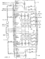
- the hybrid 65 contains two resistor strings 225 and 230 connected between differential transmitters outputs and hybrid outputs connected to the receiver input.
- the taps of the resistor string 225, 230 are connected to the differential hybrid inputs (these inputs are connected to the hybrid output of the transmitter) through transistor switches 235. Only one pair of the switches 235 can be simultaneously selected by decoder 240.
- the input of the decoder 240 is generated by the hybrid tuning block 75 shown in FIGURE 11. This block 75 chooses the switch 235 in such a way that the part of the resistor strings 225 and 230 located to the left from the chosen tap has a predetermined value of resistance. In this case, the current coming from the hybrid output of the transmitter 30 will provide the best compensation of the transmitted signal at the receiver input.
- the decoder block-diagram is shown in FIGURE 9. It decodes a three bit input code into eight output signals.
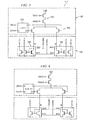
- the hybrid 65 contains a pair of resistors 245 coupling the transmitter output with the receiver.
- the value of the compensation current is adjustable. This is done by activating appropriate paths in current mirror slave transistors 250 and 255 receiving the bias voltage from master transistors 260 and 265 of the current mirror.
- the control bits ADJB ⁇ 0:2> are generated to match the compensation gain of the current mirror to the actual value of the resistors 245.
- the current mirror may introduce some dynamic distortions to the signal, the value is substantially smaller than the one that can be possible produced by the current mirror driver. This is because the current mirror gain in this case is smaller than one.
- the operating current of the hybrid current mirror can be substantially increased without affecting the power efficiency.
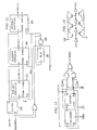
- the hybrid tuner 75 block diagram is shown in FIGURE 11.
- the hybrid tuner 75 contains comparator 275 and reversible counter 280.
- the comparator 275 receives two input currents from the bias generator 85 (FIGURE 1). One current “CURREF” is temperature and process independent. The other "CURRINT” is generated using a stable reference voltage and internal for the chip resistors. Thus, this current value is reverse proportional to the chip resistor's actual value.
- the comparator 275 receives the tuning bits ADJ ⁇ 0:2> from the counter 280. If the code of the bits corresponds to the best matching of the hybrid 65, both outputs of the comparator are low. If the bits should be changed, the comparator 275 produces either "GOUP” or “GODOWN” for the counter 280 according to the direction for the code to be changed.
- the reversible counter 280 changes its output until the comparator 275 conditions are satisfied.
- the reversible counter 280 block diagram is shown in FIGURE 12.
- the reversible counter 280 contains delay 285, which together with NOR gate 290 composes a ring oscillator; RS-latch 295, stores the direction of the count; and set of the counter cells 300. If both signals "GOUP” and “GODOWN” are low, the ring oscillator 300 is disabled. The counter output in this case remains unchanged. If either of the inputs goes “HIGH”, the ring oscillator 300 is enabled. The clock cycles are counted either upward or downward until both inputs return to "LOW.”
- the block diagrams of the up/down counter cell 280 and delay line 285 are shown in FIGURES 13 and 14 respectively.
- the schematic of the comparator 275 used for the first embodiment of the hybrid 65 is shown in FIGURE 15.
- the comparator 275 contains a replica of the hybrid resistor string 305 with switches 310 connected to the resistor taps.
- the switches 310 are controlled by a decoder 315 similar to decoder 240 (FIGURE 9).
- the selected switch applies a process independent current generated by current mirror 320 to the respective part of the resistor string 305.
- a process dependent current generated by current mirror 335 is applied to resistor 315 to create a reference voltage drop across the resistor.
- Transconductor cell 330 converts the voltage difference between the reference resistor 315 and the resistor string 305 in its output current applied to the current comparator 342.
- The. limits of the comparator are set by current sources 340a and 340b. If the transconductor current exceeds the limit, either "GOUP" or “GODOWN” goes "HIGH".
- the schematic of the comparator 275 used for the second embodiment of the hybrid 65 (Fig. 10) is shown in FIGURE 16.
- the comparator 275 contains a replica 350 of a hybrid cell.
- the replica 350 (presents the slave side) and master transistor 355 composes a current mirror, which receives a reference process independent current "CURREF".
- a process dependent current "CURRINT” is applied to the drain node of replica 350.
- Tile current difference is applied to current comparator 360, which was described above.
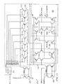
- the bias generator 85 circuit diagram is shown in FIGURE 17.
- the bias generator 85 contains two similar portions: portion 400, which is responsible for generation of the process independent reference voltages and currents; and portion 405 responsible for generation of the process dependent current. They contain external precise resistor 410, connected to an n external pin of the chip, and internal process dependent resistor 415.
- Each portion 400, 405 contains an operational amplifier 420 connected in a loop with a current source 425 and to the respective resistor 410, 415. The loop maintains the voltage drop across the resistor 430 equal to the input reference voltage. Hence, the output currents of the portions 400, 405 are reverse proportional to the respective resistor values.
- portion 400 generates the bias voltages used by other blocks of the transceiver.
Landscapes
- Engineering & Computer Science (AREA)
- Computer Networks & Wireless Communication (AREA)
- Signal Processing (AREA)
- Power Engineering (AREA)
- Dc Digital Transmission (AREA)
- Amplifiers (AREA)
- Small-Scale Networks (AREA)
Applications Claiming Priority (2)
| Application Number | Priority Date | Filing Date | Title |
|---|---|---|---|
| US10/299,273 US7176823B2 (en) | 2002-11-19 | 2002-11-19 | Gigabit ethernet line driver and hybrid architecture |
| US299273 | 2002-11-19 |
Publications (3)
| Publication Number | Publication Date |
|---|---|
| EP1422878A2 true EP1422878A2 (de) | 2004-05-26 |
| EP1422878A3 EP1422878A3 (de) | 2006-12-06 |
| EP1422878B1 EP1422878B1 (de) | 2012-08-08 |
Family
ID=32229844
Family Applications (1)
| Application Number | Title | Priority Date | Filing Date |
|---|---|---|---|
| EP03257242A Expired - Lifetime EP1422878B1 (de) | 2002-11-19 | 2003-11-18 | Leitungstreiber- und Hybridarchitektur für Gigabitethernet |
Country Status (2)
| Country | Link |
|---|---|
| US (2) | US7176823B2 (de) |
| EP (1) | EP1422878B1 (de) |
Cited By (3)
| Publication number | Priority date | Publication date | Assignee | Title |
|---|---|---|---|---|
| DE102005004369A1 (de) * | 2005-01-31 | 2006-08-10 | Infineon Technologies Ag | Verfahren und Vorrichtung zur Echokompensation eines Empfangssignals |
| EP1720306A3 (de) * | 2005-04-27 | 2007-01-17 | Broadcom Corporation | On-chip Quellenabschluss in Kommunikationssystemen |
| US7889752B2 (en) | 2003-06-05 | 2011-02-15 | Marvell International Ltd. | Dual ported network physical layer |
Families Citing this family (53)
| Publication number | Priority date | Publication date | Assignee | Title |
|---|---|---|---|---|
| US7394857B2 (en) * | 2003-10-31 | 2008-07-01 | Analog Devices, Inc. | Flexible versatile low-cost wireline transmit driver |
| US7729300B1 (en) * | 2005-08-19 | 2010-06-01 | National Semiconductor Corporation | Class-B transmitter and replica transmitter for gigabit ethernet applications |
| US7772892B2 (en) * | 2009-01-15 | 2010-08-10 | Advantest Corporation | Differential hybrid circuit |
| US9077386B1 (en) | 2010-05-20 | 2015-07-07 | Kandou Labs, S.A. | Methods and systems for selection of unions of vector signaling codes for power and pin efficient chip-to-chip communication |
| US9985634B2 (en) | 2010-05-20 | 2018-05-29 | Kandou Labs, S.A. | Data-driven voltage regulator |
| US9251873B1 (en) | 2010-05-20 | 2016-02-02 | Kandou Labs, S.A. | Methods and systems for pin-efficient memory controller interface using vector signaling codes for chip-to-chip communications |
| US9288082B1 (en) | 2010-05-20 | 2016-03-15 | Kandou Labs, S.A. | Circuits for efficient detection of vector signaling codes for chip-to-chip communication using sums of differences |
| US9252833B2 (en) * | 2012-05-07 | 2016-02-02 | Broadcom Corporation | Power efficient driver architecture |
| US8836559B2 (en) | 2012-11-29 | 2014-09-16 | Intel Mobile Communications GmbH | Capacitive digital to analog converter |
| US8674867B1 (en) * | 2012-11-29 | 2014-03-18 | Intel Mobile Communications GmbH | Capacitive radio-frequency digital-to-analog converter with a switched load |
| US8847806B2 (en) | 2012-11-29 | 2014-09-30 | Intel Mobile Communications GmbH | Digital to analog converter comprising mixer |
| CN110166217B (zh) | 2013-04-16 | 2022-05-17 | 康杜实验室公司 | 高带宽通信接口方法和系统 |
| CN105393512B (zh) | 2013-06-25 | 2019-06-28 | 康杜实验室公司 | 具有低接收器复杂度的向量信令 |
| US9419779B2 (en) * | 2013-09-06 | 2016-08-16 | Broadcom Corporation | Full-duplex driver with hybrid adaptation |
| US9806761B1 (en) | 2014-01-31 | 2017-10-31 | Kandou Labs, S.A. | Methods and systems for reduction of nearest-neighbor crosstalk |
| JP6317474B2 (ja) | 2014-02-02 | 2018-04-25 | カンドウ ラボズ ソシエテ アノニム | 制約isi比を用いる低電力チップ間通信の方法および装置 |
| EP3672176B1 (de) | 2014-02-28 | 2022-05-11 | Kandou Labs, S.A. | Vektorsignalisierungskodes mit eingebettetem takt |
| US9509437B2 (en) | 2014-05-13 | 2016-11-29 | Kandou Labs, S.A. | Vector signaling code with improved noise margin |
| US9112550B1 (en) | 2014-06-25 | 2015-08-18 | Kandou Labs, SA | Multilevel driver for high speed chip-to-chip communications |
| CN106797352B (zh) | 2014-07-10 | 2020-04-07 | 康杜实验室公司 | 高信噪特性向量信令码 |
| US9432082B2 (en) | 2014-07-17 | 2016-08-30 | Kandou Labs, S.A. | Bus reversable orthogonal differential vector signaling codes |
| CN106664272B (zh) | 2014-07-21 | 2020-03-27 | 康杜实验室公司 | 从多点通信信道接收数据的方法和装置 |
| US9461862B2 (en) | 2014-08-01 | 2016-10-04 | Kandou Labs, S.A. | Orthogonal differential vector signaling codes with embedded clock |
| US9674014B2 (en) | 2014-10-22 | 2017-06-06 | Kandou Labs, S.A. | Method and apparatus for high speed chip-to-chip communications |
| EP3314835B1 (de) | 2015-06-26 | 2020-04-08 | Kandou Labs S.A. | Hochgeschwindigkeitskommunikationssystem |
| US10055372B2 (en) | 2015-11-25 | 2018-08-21 | Kandou Labs, S.A. | Orthogonal differential vector signaling codes with embedded clock |
| WO2017132292A1 (en) | 2016-01-25 | 2017-08-03 | Kandou Labs, S.A. | Voltage sampler driver with enhanced high-frequency gain |
| US9722822B1 (en) * | 2016-03-04 | 2017-08-01 | Inphi Corporation | Method and system using driver equalization in transmission line channels with power or ground terminations |
| CN115085727B (zh) | 2016-04-22 | 2026-04-21 | 康杜实验室公司 | 高性能锁相环 |
| US10003454B2 (en) | 2016-04-22 | 2018-06-19 | Kandou Labs, S.A. | Sampler with low input kickback |
| WO2017185070A1 (en) | 2016-04-22 | 2017-10-26 | Kandou Labs, S.A. | Calibration apparatus and method for sampler with adjustable high frequency gain |
| US10153591B2 (en) | 2016-04-28 | 2018-12-11 | Kandou Labs, S.A. | Skew-resistant multi-wire channel |
| CN109417521B (zh) | 2016-04-28 | 2022-03-18 | 康杜实验室公司 | 低功率多电平驱动器 |
| CN109313622B (zh) | 2016-04-28 | 2022-04-15 | 康杜实验室公司 | 用于密集路由线组的向量信令码 |
| US10193716B2 (en) | 2016-04-28 | 2019-01-29 | Kandou Labs, S.A. | Clock data recovery with decision feedback equalization |
| US9906358B1 (en) | 2016-08-31 | 2018-02-27 | Kandou Labs, S.A. | Lock detector for phase lock loop |
| US10411922B2 (en) | 2016-09-16 | 2019-09-10 | Kandou Labs, S.A. | Data-driven phase detector element for phase locked loops |
| US10200188B2 (en) | 2016-10-21 | 2019-02-05 | Kandou Labs, S.A. | Quadrature and duty cycle error correction in matrix phase lock loop |
| US10200218B2 (en) | 2016-10-24 | 2019-02-05 | Kandou Labs, S.A. | Multi-stage sampler with increased gain |
| US10372665B2 (en) | 2016-10-24 | 2019-08-06 | Kandou Labs, S.A. | Multiphase data receiver with distributed DFE |
| TWI641253B (zh) * | 2016-12-06 | 2018-11-11 | 瑞昱半導體股份有限公司 | 網路驅動電路及網路裝置之驅動方法 |
| CN108234137B (zh) * | 2016-12-14 | 2020-10-23 | 瑞昱半导体股份有限公司 | 网络驱动电路及网络装置的驱动方法 |
| US10116468B1 (en) | 2017-06-28 | 2018-10-30 | Kandou Labs, S.A. | Low power chip-to-chip bidirectional communications |
| US10686583B2 (en) | 2017-07-04 | 2020-06-16 | Kandou Labs, S.A. | Method for measuring and correcting multi-wire skew |
| US10203226B1 (en) | 2017-08-11 | 2019-02-12 | Kandou Labs, S.A. | Phase interpolation circuit |
| US10496583B2 (en) | 2017-09-07 | 2019-12-03 | Kandou Labs, S.A. | Low power multilevel driver for generating wire signals according to summations of a plurality of weighted analog signal components having wire-specific sub-channel weights |
| US10326623B1 (en) | 2017-12-08 | 2019-06-18 | Kandou Labs, S.A. | Methods and systems for providing multi-stage distributed decision feedback equalization |
| US10554380B2 (en) | 2018-01-26 | 2020-02-04 | Kandou Labs, S.A. | Dynamically weighted exclusive or gate having weighted output segments for phase detection and phase interpolation |
| TWI730840B (zh) | 2020-07-13 | 2021-06-11 | 瑞昱半導體股份有限公司 | 回音估計系統以及回音估計方法 |
| TWI763195B (zh) | 2020-12-18 | 2022-05-01 | 瑞昱半導體股份有限公司 | 具有回音消除機制的訊號收發裝置及方法 |
| CN114744992B (zh) * | 2022-02-24 | 2025-10-14 | 裕太微(上海)电子有限公司 | 一种线路驱动器阻抗校准超压保护电路及方法 |
| US12063034B2 (en) | 2022-08-30 | 2024-08-13 | Kandou Labs SA | Line driver impedance calibration for multi-wire data bus |
| TWI819778B (zh) | 2022-09-06 | 2023-10-21 | 瑞昱半導體股份有限公司 | 通訊系統、電子裝置以及回音雜訊消除能力判斷方法 |
Family Cites Families (9)
| Publication number | Priority date | Publication date | Assignee | Title |
|---|---|---|---|---|
| US6181791B1 (en) * | 1998-01-06 | 2001-01-30 | Stmicroelectronics, Inc. | Apparatus and method for reducing local interference in subscriber loop communication system |
| ATE297623T1 (de) * | 1998-10-30 | 2005-06-15 | Broadcom Corp | Internet-gigabit-ethernet-sender-architektur |
| US6775529B1 (en) * | 2000-07-31 | 2004-08-10 | Marvell International Ltd. | Active resistive summer for a transformer hybrid |
| US6844837B1 (en) * | 2000-05-23 | 2005-01-18 | Marvell International Ltd. | Class B driver |
| US6836544B1 (en) * | 2000-08-24 | 2004-12-28 | Intel Corporation | Sidestone reduction in full duplex transceivers |
| US7027790B2 (en) * | 2001-08-10 | 2006-04-11 | Broadcom Corporation | Transceiver front-end |
| US7269254B2 (en) * | 2002-05-21 | 2007-09-11 | Silicon Laboratories, Inc. | Integrated driver circuitry |
| DE10234725B4 (de) * | 2002-07-30 | 2004-09-23 | Infineon Technologies Ag | Transceiver mit integrierter Hybrid-Schaltung |
| US20050245134A1 (en) * | 2004-04-30 | 2005-11-03 | Allied Telesyn Networks Inc. | Method and apparatus for improved data and video delivery |
-
2002
- 2002-11-19 US US10/299,273 patent/US7176823B2/en not_active Expired - Lifetime
-
2003
- 2003-11-18 EP EP03257242A patent/EP1422878B1/de not_active Expired - Lifetime
-
2007
- 2007-01-19 US US11/655,608 patent/US7327298B2/en not_active Expired - Lifetime
Cited By (8)
| Publication number | Priority date | Publication date | Assignee | Title |
|---|---|---|---|---|
| US7889752B2 (en) | 2003-06-05 | 2011-02-15 | Marvell International Ltd. | Dual ported network physical layer |
| DE102005004369A1 (de) * | 2005-01-31 | 2006-08-10 | Infineon Technologies Ag | Verfahren und Vorrichtung zur Echokompensation eines Empfangssignals |
| US7760672B2 (en) | 2005-01-31 | 2010-07-20 | Infineon Technologies Ag | Method and device for the echo compensation of a reception signal |
| DE102005004369B4 (de) * | 2005-01-31 | 2010-09-16 | Infineon Technologies Ag | Verfahren und Vorrichtung zur Echokompensation eines Empfangssignals |
| EP1720306A3 (de) * | 2005-04-27 | 2007-01-17 | Broadcom Corporation | On-chip Quellenabschluss in Kommunikationssystemen |
| US7301365B2 (en) | 2005-04-27 | 2007-11-27 | Broadcom Corporation | On-chip source termination in communication systems |
| US7576587B2 (en) | 2005-04-27 | 2009-08-18 | Broadcom Corporation | On-chip source termination in communication systems |
| US7884639B2 (en) | 2005-04-27 | 2011-02-08 | Broadcom Corporation | On-chip source termination in communication systems |
Also Published As
| Publication number | Publication date |
|---|---|
| EP1422878A3 (de) | 2006-12-06 |
| US20070127501A1 (en) | 2007-06-07 |
| US7176823B2 (en) | 2007-02-13 |
| EP1422878B1 (de) | 2012-08-08 |
| US7327298B2 (en) | 2008-02-05 |
| US20040096005A1 (en) | 2004-05-20 |
Similar Documents
| Publication | Publication Date | Title |
|---|---|---|
| EP1422878B1 (de) | Leitungstreiber- und Hybridarchitektur für Gigabitethernet | |
| US6343024B1 (en) | Self-adjustable impedance line driver with hybrid | |
| US6768443B2 (en) | Switch capacitor circuit and applications thereof | |
| US7573299B2 (en) | Semiconductor integrated circuit including output circuit | |
| JPH10304004A (ja) | 改良した物理層インターフェース装置 | |
| US7626424B2 (en) | Wireline transmission circuit | |
| US7649483B1 (en) | Communication driver | |
| WO2006120889A1 (ja) | 送信装置 | |
| US6844837B1 (en) | Class B driver | |
| US20020060587A1 (en) | Output driver for a 10baset/100basetx ethernet physical layer line interface | |
| US7095348B1 (en) | Communication driver | |
| US6489838B1 (en) | Apparatus and method for equalizing received network signals using a single zero high-pass filter having selectable impedance | |
| CN115001878A (zh) | 以太网收发器的驱动器及其控制方法和以太网收发器 | |
| US6069511A (en) | Digital slew rate and duty cycle control circuit and method | |
| US7031456B2 (en) | Method, device and system for output impedance calibration that invariably maximizes hybrid performance | |
| US7401276B2 (en) | Semiconductor device with test circuit and test method of the same | |
| US6160436A (en) | Driver with switchable gain | |
| US7869388B2 (en) | Class-B transmitter and replica transmitter for gigabit ethernet applications | |
| US6104236A (en) | Apparatus and method for equalizing received network signals using a transconductance controlled biquadratic equalizer | |
| US6545567B1 (en) | Programmable analog tapped delay line filter having cascaded differential delay cells | |
| CN210927586U (zh) | 一种隔离式igbt栅极驱动信号传输电路 | |
| US7212038B2 (en) | Line driver for transmitting data | |
| CN115189702B (zh) | 以太网发射器的驱动器及以太网发射器 | |
| US20050151565A1 (en) | Digital signal buffer circuit | |
| US6114922A (en) | Transconductance compensation for process variation in equalizers |
Legal Events
| Date | Code | Title | Description |
|---|---|---|---|
| PUAI | Public reference made under article 153(3) epc to a published international application that has entered the european phase |
Free format text: ORIGINAL CODE: 0009012 |
|
| AK | Designated contracting states |
Kind code of ref document: A2 Designated state(s): AT BE BG CH CY CZ DE DK EE ES FI FR GB GR HU IE IT LI LU MC NL PT RO SE SI SK TR |
|
| AX | Request for extension of the european patent |
Extension state: AL LT LV MK |
|
| PUAL | Search report despatched |
Free format text: ORIGINAL CODE: 0009013 |
|
| AK | Designated contracting states |
Kind code of ref document: A3 Designated state(s): AT BE BG CH CY CZ DE DK EE ES FI FR GB GR HU IE IT LI LU MC NL PT RO SE SI SK TR |
|
| AX | Request for extension of the european patent |
Extension state: AL LT LV MK |
|
| RIC1 | Information provided on ipc code assigned before grant |
Ipc: H04L 12/413 20060101AFI20040315BHEP Ipc: H04L 25/02 20060101ALI20061031BHEP |
|
| 17P | Request for examination filed |
Effective date: 20070601 |
|
| AKX | Designation fees paid |
Designated state(s): DE FR GB IT |
|
| 17Q | First examination report despatched |
Effective date: 20071213 |
|
| GRAP | Despatch of communication of intention to grant a patent |
Free format text: ORIGINAL CODE: EPIDOSNIGR1 |
|
| RIN1 | Information on inventor provided before grant (corrected) |
Inventor name: ZABRODA, OLEKSIY |
|
| GRAS | Grant fee paid |
Free format text: ORIGINAL CODE: EPIDOSNIGR3 |
|
| GRAA | (expected) grant |
Free format text: ORIGINAL CODE: 0009210 |
|
| AK | Designated contracting states |
Kind code of ref document: B1 Designated state(s): DE FR GB IT |
|
| REG | Reference to a national code |
Ref country code: GB Ref legal event code: FG4D |
|
| REG | Reference to a national code |
Ref country code: DE Ref legal event code: R096 Ref document number: 60341726 Country of ref document: DE Effective date: 20121011 |
|
| PG25 | Lapsed in a contracting state [announced via postgrant information from national office to epo] |
Ref country code: IT Free format text: LAPSE BECAUSE OF FAILURE TO SUBMIT A TRANSLATION OF THE DESCRIPTION OR TO PAY THE FEE WITHIN THE PRESCRIBED TIME-LIMIT Effective date: 20120808 |
|
| PLBE | No opposition filed within time limit |
Free format text: ORIGINAL CODE: 0009261 |
|
| STAA | Information on the status of an ep patent application or granted ep patent |
Free format text: STATUS: NO OPPOSITION FILED WITHIN TIME LIMIT |
|
| 26N | No opposition filed |
Effective date: 20130510 |
|
| GBPC | Gb: european patent ceased through non-payment of renewal fee |
Effective date: 20121118 |
|
| REG | Reference to a national code |
Ref country code: DE Ref legal event code: R097 Ref document number: 60341726 Country of ref document: DE Effective date: 20130510 |
|
| PG25 | Lapsed in a contracting state [announced via postgrant information from national office to epo] |
Ref country code: GB Free format text: LAPSE BECAUSE OF NON-PAYMENT OF DUE FEES Effective date: 20121118 |
|
| REG | Reference to a national code |
Ref country code: FR Ref legal event code: PLFP Year of fee payment: 13 |
|
| REG | Reference to a national code |
Ref country code: FR Ref legal event code: PLFP Year of fee payment: 14 |
|
| REG | Reference to a national code |
Ref country code: FR Ref legal event code: PLFP Year of fee payment: 15 |
|
| REG | Reference to a national code |
Ref country code: FR Ref legal event code: PLFP Year of fee payment: 16 |
|
| PGFP | Annual fee paid to national office [announced via postgrant information from national office to epo] |
Ref country code: FR Payment date: 20181024 Year of fee payment: 16 |
|
| REG | Reference to a national code |
Ref country code: DE Ref legal event code: R082 Ref document number: 60341726 Country of ref document: DE Representative=s name: PAGE, WHITE & FARRER GERMANY LLP, DE |
|
| PG25 | Lapsed in a contracting state [announced via postgrant information from national office to epo] |
Ref country code: FR Free format text: LAPSE BECAUSE OF NON-PAYMENT OF DUE FEES Effective date: 20191130 |
|
| PGFP | Annual fee paid to national office [announced via postgrant information from national office to epo] |
Ref country code: DE Payment date: 20201020 Year of fee payment: 18 |
|
| REG | Reference to a national code |
Ref country code: DE Ref legal event code: R119 Ref document number: 60341726 Country of ref document: DE |
|
| PG25 | Lapsed in a contracting state [announced via postgrant information from national office to epo] |
Ref country code: DE Free format text: LAPSE BECAUSE OF NON-PAYMENT OF DUE FEES Effective date: 20220601 |