EP1423907B1 - Stromversorgung für die induktionserwärmung oder schmelzung - Google Patents
Stromversorgung für die induktionserwärmung oder schmelzung Download PDFInfo
- Publication number
- EP1423907B1 EP1423907B1 EP02753445.2A EP02753445A EP1423907B1 EP 1423907 B1 EP1423907 B1 EP 1423907B1 EP 02753445 A EP02753445 A EP 02753445A EP 1423907 B1 EP1423907 B1 EP 1423907B1
- Authority
- EP
- European Patent Office
- Prior art keywords
- output
- load coil
- inductive load
- inverter
- power supply
- Prior art date
- Legal status (The legal status is an assumption and is not a legal conclusion. Google has not performed a legal analysis and makes no representation as to the accuracy of the status listed.)
- Expired - Lifetime
Links
- 238000010438 heat treatment Methods 0.000 title claims description 15
- 238000002844 melting Methods 0.000 title claims description 14
- 230000008018 melting Effects 0.000 title claims description 14
- 230000006698 induction Effects 0.000 title description 24
- 239000003990 capacitor Substances 0.000 claims description 30
- 230000001939 inductive effect Effects 0.000 claims description 24
- 239000004020 conductor Substances 0.000 claims description 7
- 238000000034 method Methods 0.000 claims description 7
- 230000008878 coupling Effects 0.000 claims description 3
- 238000010168 coupling process Methods 0.000 claims description 3
- 238000005859 coupling reaction Methods 0.000 claims description 3
- 238000003079 width control Methods 0.000 claims description 3
- 238000001914 filtration Methods 0.000 claims description 2
- 238000010586 diagram Methods 0.000 description 8
- 239000002184 metal Substances 0.000 description 4
- 239000007787 solid Substances 0.000 description 4
- 230000008901 benefit Effects 0.000 description 3
- 230000000694 effects Effects 0.000 description 1
- 238000012986 modification Methods 0.000 description 1
- 230000004048 modification Effects 0.000 description 1
- 238000004804 winding Methods 0.000 description 1
Images



Classifications
-
- H—ELECTRICITY
- H05—ELECTRIC TECHNIQUES NOT OTHERWISE PROVIDED FOR
- H05B—ELECTRIC HEATING; ELECTRIC LIGHT SOURCES NOT OTHERWISE PROVIDED FOR; CIRCUIT ARRANGEMENTS FOR ELECTRIC LIGHT SOURCES, IN GENERAL
- H05B6/00—Heating by electric, magnetic or electromagnetic fields
- H05B6/02—Induction heating
- H05B6/06—Control, e.g. of temperature, of power
- H05B6/067—Control, e.g. of temperature, of power for melting furnaces
-
- H—ELECTRICITY
- H02—GENERATION; CONVERSION OR DISTRIBUTION OF ELECTRIC POWER
- H02M—APPARATUS FOR CONVERSION BETWEEN AC AND AC, BETWEEN AC AND DC, OR BETWEEN DC AND DC, AND FOR USE WITH MAINS OR SIMILAR POWER SUPPLY SYSTEMS; CONVERSION OF DC OR AC INPUT POWER INTO SURGE OUTPUT POWER; CONTROL OR REGULATION THEREOF
- H02M5/00—Conversion of AC power input into AC power output, e.g. for change of voltage, for change of frequency, for change of number of phases
- H02M5/40—Conversion of AC power input into AC power output, e.g. for change of voltage, for change of frequency, for change of number of phases with intermediate conversion into DC
- H02M5/42—Conversion of AC power input into AC power output, e.g. for change of voltage, for change of frequency, for change of number of phases with intermediate conversion into DC by static converters
- H02M5/44—Conversion of AC power input into AC power output, e.g. for change of voltage, for change of frequency, for change of number of phases with intermediate conversion into DC by static converters using discharge tubes or semiconductor devices to convert the intermediate DC into AC
- H02M5/453—Conversion of AC power input into AC power output, e.g. for change of voltage, for change of frequency, for change of number of phases with intermediate conversion into DC by static converters using discharge tubes or semiconductor devices to convert the intermediate DC into AC using devices of a triode or transistor type requiring continuous application of a control signal
- H02M5/458—Conversion of AC power input into AC power output, e.g. for change of voltage, for change of frequency, for change of number of phases with intermediate conversion into DC by static converters using discharge tubes or semiconductor devices to convert the intermediate DC into AC using devices of a triode or transistor type requiring continuous application of a control signal using semiconductor devices only
-
- H—ELECTRICITY
- H05—ELECTRIC TECHNIQUES NOT OTHERWISE PROVIDED FOR
- H05B—ELECTRIC HEATING; ELECTRIC LIGHT SOURCES NOT OTHERWISE PROVIDED FOR; CIRCUIT ARRANGEMENTS FOR ELECTRIC LIGHT SOURCES, IN GENERAL
- H05B6/00—Heating by electric, magnetic or electromagnetic fields
- H05B6/02—Induction heating
- H05B6/04—Sources of current
-
- H—ELECTRICITY
- H02—GENERATION; CONVERSION OR DISTRIBUTION OF ELECTRIC POWER
- H02M—APPARATUS FOR CONVERSION BETWEEN AC AND AC, BETWEEN AC AND DC, OR BETWEEN DC AND DC, AND FOR USE WITH MAINS OR SIMILAR POWER SUPPLY SYSTEMS; CONVERSION OF DC OR AC INPUT POWER INTO SURGE OUTPUT POWER; CONTROL OR REGULATION THEREOF
- H02M7/00—Conversion of AC power input into DC power output; Conversion of DC power input into AC power output
- H02M7/42—Conversion of DC power input into AC power output without possibility of reversal
- H02M7/44—Conversion of DC power input into AC power output without possibility of reversal by static converters
- H02M7/48—Conversion of DC power input into AC power output without possibility of reversal by static converters using discharge tubes with control electrode or semiconductor devices with control electrode
- H02M7/4815—Resonant converters
-
- Y—GENERAL TAGGING OF NEW TECHNOLOGICAL DEVELOPMENTS; GENERAL TAGGING OF CROSS-SECTIONAL TECHNOLOGIES SPANNING OVER SEVERAL SECTIONS OF THE IPC; TECHNICAL SUBJECTS COVERED BY FORMER USPC CROSS-REFERENCE ART COLLECTIONS [XRACs] AND DIGESTS
- Y02—TECHNOLOGIES OR APPLICATIONS FOR MITIGATION OR ADAPTATION AGAINST CLIMATE CHANGE
- Y02B—CLIMATE CHANGE MITIGATION TECHNOLOGIES RELATED TO BUILDINGS, e.g. HOUSING, HOUSE APPLIANCES OR RELATED END-USER APPLICATIONS
- Y02B70/00—Technologies for an efficient end-user side electric power management and consumption
- Y02B70/10—Technologies improving the efficiency by using switched-mode power supplies [SMPS], i.e. efficient power electronics conversion e.g. power factor correction or reduction of losses in power supplies or efficient standby modes
Definitions
- the present invention relates to an ac power supply for use in induction heating or melting applications wherein the induction power circuit is resonantly tuned.
- US 6,141,227 discloses a power supply according to the preamble of claim 1.
- FIG. 1 illustrates a conventional power supply 110 that is used in induction heating or melting applications.
- the power supply consists of an ac-to-dc rectifier and filter section 112, a dc-to-ac inverter section 120 and a tuning capacitor section 130.
- a three-phase diode bridge rectifier 114 converts three-phase (A, B, C) ac utility line power into dc power.
- Current limiting reactor L 108 smoothes out the ripple in the output dc current of the rectifier, and capacitor C 108 filters the ac component from the output dc voltage of the rectifier.
- the filtered dc output of the rectifier is inverted to ac by a full-bridge inverter consisting of solid state switches S 101 , S 102 , S 103 and S 104 and associated antiparallel diodes D 101 , D 102 , D 103 and D 104 , respectively. Alternating turn-on/turn-off cycles of switch pairs S 101 /S 103 and S 102 /S 104 produce a synthesized ac inverter output at terminals 3 and 4.
- Induction load coil L 101 represents the power coil used in the induction heating or melting application.
- load coil L 101 is wound around the exterior of a crucible in which metal charge has been placed.
- a metal workpiece such as a strip or wire, may travel through a helical winding of load coil L 101 or otherwise be brought near to the coil to inductively heat the workpiece.
- Current supplied by the power supply and flowing through load coil L 101 creates a magnetic field that either directly heats the metal charge or workpiece by magnetic induction, or heats the workpiece by heat conduction from a susceptor that is heated by magnetic induction.
- Load coil L 101 whether it be a single coil or an assembly of interconnected coil sections, has a very low operating power factor. Because of this, a tuning capacitor (or bank of capacitors), such as capacitor C 101 must be provided in the load coil circuit to improve the overall power factor of the load coil circuit. These tuning capacitors are a significant cost and volume component of the power supply. Therefore, there exists the need for a power supply for inductive heating or melting applications that utilizes smaller and less costly tuning capacitors.
- An objective of the present invention is to provide a power supply for inductive heating or melting applications that utilizes a capacitor connected between the output of the rectifier and the input of the inverter to form a resonantly tuned circuit with the induction load coil used in the application.
- the invention refers to a device according to claim 1 and to a method according to claim 6.
- the present invention is apparatus for, and a method of, providing a power supply with rectifier and inverter sections for use with an induction load coil wherein a tuning capacitor is provided across the output of the rectifier and the input of the inverter to form a resonant circuit with the induction load coil.
- the induction load coil may comprise an active load coil connected to the output of the inverter, and a passive load coil connected in parallel with a capacitor to form a tank circuit.
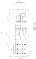
- FIG. 2 an illustration of one example of power supply 10 of the present invention for use in induction heating or melting applications.
- Ac-to-dc rectifier and filter section 12 includes an ac-to-dc rectifier.
- a multi-phase rectifier in this non-limiting example of the invention, a three-phase diode bridge rectifier 14 is used to convert three-phase (A, B, C) ac utility line power into dc power.
- Optional current limiting reactor L 8 smoothes out the ripple from the output dc current of the rectifier.
- Section 16 of the power supply diagrammatically illustrates coil tuning capacitor C 1 , which can be a single capacitor or a bank of interconnected capacitors that form a capacitive element.
- the dc output of the rectifier is supplied to input terminals 1 and 2 of a full-bridge inverter in inverter section 20.
- the inverter consists of solid state switches S 1 , S 2 , S 3 and S 4 and associated antiparallel diodes D 1 , D 2 , D 3 and D 4 , respectively. Alternating turn-on/turn-off cycles of switch pairs S 1 /S 3 and S 2 /S 4 produce a synthesized ac inverter output at terminals 3 and 4.
- a preferred, but not limiting, choice of component for the solid state switch is an isolated gate bipolar transistor (IGBT), which exhibits the desirable characteristics of power bipolar transistors and power MOS-FETs at high operating voltages and currents.
- IGBT isolated gate bipolar transistor
- the inverter employs a phase-shifting scheme (pulse width control) relative to the turn-on/turn-off cycles of the two switch pairs whereby variable overlapping on-times for the two switch pairs is used to vary the effective RMS output voltage of the inverter.
- phase-shifting scheme pulse width control
- Induction load coil L 9 represents the power coil used in the induction heating or melting apparatus.
- the capacitance of capacitor C 1 is selected to form a resonant circuit with the impedance of load coil L 9 at the operating frequency of the inverter, which is the switching rate of the switch pairs used in the inverter. Consequently, a tuning capacitor is not required at the output of the inverter. Selection of available circuit components may not allow operation exactly at resonance, but as close to resonance as is achievable with available components.
- the ac current flowing through induction load coil L 9 from the output of the inverter magnetically couples with an electrically conductive material, which may be, for example, a conductive metal or a susceptor.
- FIG. 3 through FIG. 5 illustrate the performance characteristics for power supply 10 of the present invention as shown in FIG. 2 with input utility line power (A, B, C) of 480 volts line-to-line, 60 Hertz, and inverter 20 operating at an output frequency of 60 Hz.
- input utility line power A, B, C
- inverter 20 operating at an output frequency of 60 Hz.
- L 8 is selected as 5,000 ⁇ H (for an impedance of 3.77 ohms at the rectifier ripple output frequency of 120 Hz);
- C 1 is selected as 5,000 ⁇ F (for an impedance of 0.27 ohms at the rectifier ripple output frequency of 120 Hz);
- L 9 is selected as 1,000 ⁇ H (for an impedance of 0.38 ohms at the inverter output frequency of 60 Hz).
- FIG. 4 graphically illustrates that the voltage across capacitor C 1 , namely V C1 , is driven to its limiting lower value of zero volts as a result of capacitor C 1 being in resonance with coil L 9 at the ripple frequency of 120 Hz.
- V C1 is the applied voltage to the input of inverter 20 (at terminals 1 and 2 ).
- FIG. 4 also illustrates the ripple current, I L8 , through reactor L 8 .
- the impedance of reactor L 8 is generally selected to be much greater than the impedance of C 1 to block feedback of harmonics from the inverter circuit to the rectifier's power source.
- FIG. 5 graphically illustrates the voltage, V s , across one of the solid state switches in inverter 20, and the current, I S , through one of the switches at maximum power output when there is zero overlap angle between V s and I s .
- Switching device turn-off at zero volts for V s when dc ripple has reached zero (e.g., at 240.0 milliseconds (ms) in FIG. 4 and FIG. 5 ), will minimize switching loses.
- any spikes due to stray circuit inductance will be significantly less than in a conventional inverter having low ac ripple current in the dc link voltage.
- FIG. 6 illustrates a second example of the present invention.
- the load coil consists of an active coil L 1 and at least one passive coil L 2 .
- Coils L 1 and L 2 may be wound in one of various configurations, such as sequentially or overlapped, to accomplish mutual magnetic coupling of the coils as further described below.
- Coil L 1 is connected to the output of inverter 20.
- Coil L 2 is connected in parallel with resonant tuning capacitor C 2 to form a parallel tank resonant circuit.
- Coil L 2 is not physically connected to coil L 1 .
- the parallel tank resonant circuit is energized by magnetically coupling coil L 2 with the magnetic field generated in coil L 1 when current supplied from the output of inverter 20 flows through coil L 1 .
- vector OV represents current I 1 in active coil L 1 as illustrated FIG. 6 .
- Vector OA represents the resistive component of the active coil's voltage, I 1 R 1 ( R 1 not shown in the figures).
- Vector AB represents the inductive component of the active coil's voltage, ⁇ L 1 I 1 (where ⁇ equals the product of 2 ⁇ and f, the operating frequency of the power supply).
- Vector BC represents the voltage, ⁇ MI 2 , induced by the passive coil L 2 onto active coil L 1 .
- V C1 across capacitor C 1 and the switching function of the two switch pairs S 1 /S 3 and S 2 /S 4 produce the effect of a pseudo capacitor C 1 ' connected in series with L 1 that would result in a sinusoidal voltage at terminals 5 and 6 in FIG. 6 .
- Vector CD represents the voltage, I 1 / ⁇ C 1 ', that would appear across this pseudo series capacitor C 1 '.
- Vector OD represents the output voltage, V inv , of the inverter (terminals 3 and 4 in FIG. 6 ).
- vector OW represents current I 2 in passive coil L 2 that is induced by the magnetic field produced by current I 1 .
- Vector OF represents the resistive component of the passive coil's voltage, I 2 R 2 (R 2 not shown in the figures).
- Vector FE represents the inductive component of the active coil's voltage, ⁇ L 2 I 2 .
- Vector EG represents the voltage, ⁇ MI 1 , induced by the active coil L 1 onto passive coil L 2 .
- Vector GO represents the voltage, I 2 / ⁇ C 2 , on capacitor C 2 , which is connected across passive coil L 2 .
- the active coil circuit is driven by the voltage source, V inv , which is the output of inverter 20, while the passive coil loop is not connected to an active energy source. Since the active and passive coils are mutually coupled, vector BC is added to vector OB, V' LOAD , which represents the voltage across an active induction load coil in the absence of a passive capacitive load coil circuit, to result in vector OC, V LOAD , which is the voltage across an active load coil with a passive capacitive load coil circuit of the present invention.
- the resultant load voltage, V LOAD has a smaller lagging power factor angle, ⁇ (counterclockwise angle between the x-axis and vector OC ), than the conventional load coil as represented by vector OB. As illustrated in FIG. 7 , there is a power factor angle improvement of ⁇ .
- the uncompensated resistive component, R 2 in the passive coil circuit is reflected into the active coil circuit by the mutual inductance between the two circuits, and the effective active coil circuit's resistance is increased, thus improving the power factor angle, or efficiency of the coil system.
- the power factor angle, ⁇ for the output of the inverter improves by ⁇ as illustrated by the angle between vector OJ, V' inv (resultant vector of resistive component vector OA and capacitive component vector AJ in the absence of a passive load coil circuit) and vector OD, V inv (resultant vector of resistive component vector OH and capacitive component vector HD with a passive load coil circuit of the present invention).
- multiple active and/or passive coil circuits may be used to achieve a desired multiple coil arrangement for a particular application.
- the examples of the invention include reference to specific electrical components.
- One skilled in the art may practice the invention by substituting components that are not necessarily of the same type but will create the desired conditions or accomplish the desired results of the invention.
- single components may be substituted for multiple components or vice versa.
- one skilled in the art may practice the invention by rearranging components to create the desired conditions or accomplish the desired results of the invention.
- the examples illustrate operation of the invention in full-bridge voltage-fed power supplies, the invention is applicable to other power supply topologies with appropriate modifications as understood by one who is skilled in the art.
Landscapes
- Physics & Mathematics (AREA)
- Electromagnetism (AREA)
- Engineering & Computer Science (AREA)
- Power Engineering (AREA)
- General Induction Heating (AREA)
- Inverter Devices (AREA)
Claims (9)
- Leistungsversorgung (10) zum induktiven Erwärmen oder Schmelzen eines elektrisch leitfähigen Materials, wobei die Leistungsversorgung Folgendes umfasst:einen Gleichrichter (14), der eine Wechselstrom-Eingangsleistung in eine Gleichstrom-Ausgangsleistung am Ausgang des Gleichrichters umwandelt;einen Wechselrichter (20), der einen mit dem Ausgang des Gleichrichters verbundenen Eingang umfasst, wobei der Wechselrichter die Gleichstrom-Ausgangsleistung des Gleichrichters in einen an einen Ausgang der Leistungsversorgung zugeführten Ausgangs-Wechselstrom umwandelt, wobei der Ausgangs-Wechselstrom eine Frequenz aufweist, die der Betriebsfrequenz des Wechselrichters gleich ist; undmindestens eine induktive Lastspule (L9; L1, L2), die mit dem Ausgang der Leistungsversorgung verbunden ist,dadurch gekennzeichnet, dassmindestens ein Abstimmkondensator (C1) an dem Ausgang des Gleichrichters und dem Eingang des Wechselrichters angeschlossen ist, wobei die mindestens eine induktive Lastspule eine derartige Induktivität aufweist, dass sie sich bei der Betriebsfrequenz des Wechselrichters mindestens ungefähr mit dem mindestens einen Abstimmkondensator in Resonanz befindet, wodurch beim Gebrauch der Leistungsversorgung ein von dem Fluss des Ausgangs-Wechselstroms durch die mindestens eine induktive Lastspule erzeugtes Magnetfeld verwendet wird, um ein elektrisch leitfähiges Material zu erwärmen oder zu schmelzen.
- Leistungsversorgung nach Anspruch 1, wobei die mindestens eine induktive Lastspule eine mit dem Ausgang der Leistungsversorgung verbundene erste induktive Lastspule (L1) und mindestens eine zweite induktive Lastspule (L2) umfasst, wobei die mindestens eine zweite induktive Lastspule nicht mit der ersten induktiven Lastspule verbunden ist, wobei die mindestens eine zweite induktive Lastspule mit mindestens einem ResonanzAbstimmkondensator (C2) parallel geschaltet ist, um einen Parallel-Resonanzschwingkreis zu bilden, wobei die zweite induktive Lastspule magnetisch mit der ersten induktiven Lastspule gekoppelt ist, wenn beim Gebrauch der Leistungsversorgung der Ausgangs-Wechselstrom durch die erste induktive Lastspule fließt, um einen Sekundär-Wechselstrom in dem Parallel-Resonanzschwingkreis zu induzieren, wobei die Impedanz der Kombination der ersten induktiven Lastspule und des Parallel-Resonanzschwingkreises sich bei der Betriebsfrequenz des Wechselrichters mindestens ungefähr mit der Impedanz des mindestens einen Abstimmkondensators in Resonanz befindet, wodurch beim Gebrauch der Leistungsversorgung ein von dem Fluss des Ausgangs-Wechselstroms durch die erste induktive Lastspule erzeugtes erstes Magnetfeld und ein von dem Fluss des Sekundär-Wechselstroms in dem Parallel-Resonanzschwingkreis erzeugtes zweites Magnetfeld verwendet werden, um ein elektrisch leitfähiges Material zu Erwärmen oder zu schmelzen.
- Leistungsversorgung nach Anspruch 1 oder 2, umfassend eine mit dem Ausgang des Gleichrichters in Reihe geschaltete Strombegrenzungsdrossel (L8).
- Leistungsversorgung nach Anspruch 1 oder 2, die Pulsbreitensteuerung verwendet, um die Ausgangsspannung des Wechselrichters zu verändern.
- Leistungsversorgung nach Anspruch 1 oder 2, wobei der Wechselrichter mindestens ein Paar (S1/S3, S2/S4) bipolarer Transistoren mit isoliertem Gate umfasst, wobei jeder der bipolaren Transistoren mit isoliertem Gate mit einer antiparallelen Diode (D1/D3, D2/D4) antiparallel geschaltet ist, um den Ausgangs-Wechselstrom zu erzeugen.
- Verfahren zum induktiven Erwärmen oder Schmelzen eines elektrisch leitfähigen Materials, wobei das Verfahren folgende Schritte umfasst:Gleichrichten einer Wechselstrom-Eingangsleistung in eine Gleichstrom-Ausgangsleistung;Umrichten der Gleichstrom-Ausgangsleistung, um in einem Wechselrichter (20) einen Ausgangs-Wechselstrom mit einer Betriebsfrequenz des Wechselrichters zu erzeugen; undAnlegen des Ausgangs-Wechselstroms an mindestens eine induktive Lastspule (L9), um ein Magnetfeld zu erzeugen, das magnetisch mit dem elektrisch leitfähigen Material koppelt, um das elektrisch leitfähige Material induktiv zu erwärmen oder zu schmelzen;gekennzeichnet durch den folgenden Schritt:Bilden eines bei der Betriebsfrequenz des Wechselrichters mindestens ungefähr resonanten Stromkreises mit der mindestens einen induktiven Lastspule (L9) und mindestens einem, an dem Gleichstrom-Leistungsausgang angeordneten Abstimmkondensator (C2).
- Verfahren nach Anspruch 6, umfassend den Schritt des induktiven Koppelns einer zweiten induktiven Lastspule (L2) mit dem Magnetfeld, wobei die zweite induktive Lastspule mit mindestens einem Resonanzabstimmkondensator (C2) parallel geschaltet ist, um einen Parallel-Resonanzschwingkreis zu bilden, um dadurch einen bei der Betriebsfrequenz des Wechselrichters mindestens ungefähr resonanten Kreis mit der Impedanz der Kombination der mindestens einen induktiven Lastspule und des Parallel-Resonanzschwingkreises, und dem mindestens einen, an dem Gleichstrom-Leistungsausgang angeordneten Abstimmkondensator zu bilden.
- Verfahren nach Anspruch 6 oder 7, umfassend den Schritt des Filterns des Stroms des Gleichstrom-Leistungsausgangs.
- Verfahren nach Anspruch 6 oder 7, umfassend den Schritt des Veränderns der Ausgangsspannung des Wechselrichters mit Pulsbreitensteuerung.
Applications Claiming Priority (3)
| Application Number | Priority Date | Filing Date | Title |
|---|---|---|---|
| US31215901P | 2001-08-14 | 2001-08-14 | |
| US312159P | 2001-08-14 | ||
| PCT/US2002/025414 WO2003017456A1 (en) | 2001-08-14 | 2002-08-12 | Power supply for induction heating or melting |
Publications (3)
| Publication Number | Publication Date |
|---|---|
| EP1423907A1 EP1423907A1 (de) | 2004-06-02 |
| EP1423907A4 EP1423907A4 (de) | 2008-11-19 |
| EP1423907B1 true EP1423907B1 (de) | 2016-02-17 |
Family
ID=23210137
Family Applications (1)
| Application Number | Title | Priority Date | Filing Date |
|---|---|---|---|
| EP02753445.2A Expired - Lifetime EP1423907B1 (de) | 2001-08-14 | 2002-08-12 | Stromversorgung für die induktionserwärmung oder schmelzung |
Country Status (11)
| Country | Link |
|---|---|
| US (1) | US6696770B2 (de) |
| EP (1) | EP1423907B1 (de) |
| JP (1) | JP4092293B2 (de) |
| KR (1) | KR101021560B1 (de) |
| CN (1) | CN100361380C (de) |
| AU (1) | AU2002313733B2 (de) |
| BR (1) | BR0211940A (de) |
| CA (1) | CA2456473A1 (de) |
| ES (1) | ES2565452T3 (de) |
| MX (1) | MXPA04001390A (de) |
| WO (1) | WO2003017456A1 (de) |
Families Citing this family (27)
| Publication number | Priority date | Publication date | Assignee | Title |
|---|---|---|---|---|
| US6992406B2 (en) * | 2001-08-14 | 2006-01-31 | Inductotherm Corp. | Induction heating or melting power supply utilizing a tuning capacitor |
| US7034263B2 (en) | 2003-07-02 | 2006-04-25 | Itherm Technologies, Lp | Apparatus and method for inductive heating |
| US7279665B2 (en) * | 2003-07-02 | 2007-10-09 | Itherm Technologies, Lp | Method for delivering harmonic inductive power |
| US7022952B2 (en) * | 2003-08-26 | 2006-04-04 | General Electric Company | Dual coil induction heating system |
| US7772530B2 (en) * | 2004-10-30 | 2010-08-10 | Inductotherm Corp. | Induction heat treatment of workpieces |
| US9370049B2 (en) * | 2004-12-08 | 2016-06-14 | Inductotherm Corp. | Electric induction heating, melting and stirring of materials non-electrically conductive in the solid state |
| EP1829426B1 (de) * | 2004-12-08 | 2012-03-07 | Inductotherm Corp. | Elektrisches induktionssteuersystem |
| US7582851B2 (en) * | 2005-06-01 | 2009-09-01 | Inductotherm Corp. | Gradient induction heating of a workpiece |
| SI1917713T1 (sl) * | 2005-08-25 | 2018-11-30 | Consarc Corporation | Nadzor izhoda električnega pretvornika z modulirano impulzno širino |
| JP4441691B2 (ja) * | 2007-02-06 | 2010-03-31 | 国立大学法人東京工業大学 | 交流/直流電力変換装置 |
| CN101658066B (zh) * | 2007-04-07 | 2012-09-05 | 应达公司 | 用于电感应加热、熔化和搅拌的具有脉冲调节器的电流反馈逆变器 |
| WO2009058820A2 (en) * | 2007-11-03 | 2009-05-07 | Inductotherm Corp. | Electric power system for electric induction heating and melting of materials in a susceptor vessel |
| EP2112862B1 (de) * | 2008-04-25 | 2013-04-10 | Electrolux Home Products Corporation N.V. | Verfahren und Anordnung zur dynamischen Wellenformkorrektur |
| CN102204076A (zh) * | 2008-10-27 | 2011-09-28 | 莫斯科技株式会社 | 电力逆转换装置 |
| CN102564125A (zh) * | 2011-04-20 | 2012-07-11 | 泰州杰利瑞节能科技发展有限公司 | 一种超音频感应加热熔炼炉 |
| EP2546969A1 (de) * | 2011-07-14 | 2013-01-16 | Siemens Aktiengesellschaft | Verfahren zur Steuerung eines Frequenzumrichters und Frequenzumrichter |
| US10605464B2 (en) | 2012-10-15 | 2020-03-31 | Whirlpool Corporation | Induction cooktop |
| ITTO20120896A1 (it) | 2012-10-15 | 2014-04-16 | Indesit Co Spa | Piano cottura a induzione |
| AU2015311645B2 (en) | 2014-09-05 | 2018-07-05 | Kenyon International, Inc. | Induction cooking appliance |
| US9677700B2 (en) | 2014-10-27 | 2017-06-13 | Ajax Tocco Magnethermic Corporation | Pipe heating apparatus and methods for uniform end heating and controlled heating length |
| JP2016158344A (ja) * | 2015-02-24 | 2016-09-01 | 株式会社日立製作所 | 電力変換装置およびエレベータ |
| ITUB20152674A1 (it) | 2015-07-30 | 2017-01-30 | Danieli Automation Spa | Apparato e metodo di alimentazione elettrica di un forno elettrico ad arco |
| EP3432682B1 (de) | 2017-07-18 | 2026-04-08 | Whirlpool Corporation | Verfahren zum betreiben eines induktionskochfelds und kochfeld mit diesem verfahren |
| US10993292B2 (en) | 2017-10-23 | 2021-04-27 | Whirlpool Corporation | System and method for tuning an induction circuit |
| US11140751B2 (en) | 2018-04-23 | 2021-10-05 | Whirlpool Corporation | System and method for controlling quasi-resonant induction heating devices |
| US12302478B2 (en) | 2018-04-23 | 2025-05-13 | Whirlpool Corporation | Control circuits and methods for distributed induction heating devices |
| US12588112B2 (en) | 2018-04-23 | 2026-03-24 | Whirlpool Corporation | System and method for controlling induction heating devices with series connected switching devices |
Family Cites Families (9)
| Publication number | Priority date | Publication date | Assignee | Title |
|---|---|---|---|---|
| US4115676A (en) * | 1976-02-10 | 1978-09-19 | Tokyo Shibaura Electric Co., Ltd. | Induction heating apparatus |
| US4426564A (en) * | 1979-12-26 | 1984-01-17 | General Electric Company | Parallel resonant induction cooking surface unit |
| US4638138A (en) * | 1984-07-23 | 1987-01-20 | Westinghouse Electric Corp. | High frequency inverter circuit for melting and induction heating |
| FR2680922B1 (fr) * | 1991-08-26 | 1995-02-17 | Electricite De France | Procede de regulation d'un onduleur de tension fonctionnant en quasi-resonance. |
| DE19527827C2 (de) | 1995-07-29 | 1998-02-12 | Kuka Schweissanlagen & Roboter | Verfahren und Einrichtung zur Erzeugung elektrischer Wärme |
| US5968398A (en) * | 1997-05-16 | 1999-10-19 | The Lepel Corporation | Apparatus and method for non-contact detection and inductive heating of heat retentive food server warming plates |
| DE19731690C2 (de) * | 1997-07-23 | 1999-10-28 | Siemens Ag | Leistungsverstärker und Kernspintomograph |
| GB2350733B (en) * | 1999-06-03 | 2003-02-12 | Cheltenham Induction Heating L | Power supply |
| DE60224374T2 (de) * | 2001-02-16 | 2008-12-18 | Inductotherm Corp. | Gleichzeitige induktionserwärmung und rühren eines geschmolzenen metalls |
-
2002
- 2002-08-12 CN CNB028160398A patent/CN100361380C/zh not_active Expired - Lifetime
- 2002-08-12 JP JP2003522249A patent/JP4092293B2/ja not_active Expired - Lifetime
- 2002-08-12 MX MXPA04001390A patent/MXPA04001390A/es active IP Right Grant
- 2002-08-12 US US10/217,081 patent/US6696770B2/en not_active Expired - Lifetime
- 2002-08-12 WO PCT/US2002/025414 patent/WO2003017456A1/en not_active Ceased
- 2002-08-12 KR KR1020047002246A patent/KR101021560B1/ko not_active Expired - Lifetime
- 2002-08-12 EP EP02753445.2A patent/EP1423907B1/de not_active Expired - Lifetime
- 2002-08-12 BR BR0211940-4A patent/BR0211940A/pt not_active IP Right Cessation
- 2002-08-12 AU AU2002313733A patent/AU2002313733B2/en not_active Expired
- 2002-08-12 CA CA002456473A patent/CA2456473A1/en not_active Abandoned
- 2002-08-12 ES ES02753445.2T patent/ES2565452T3/es not_active Expired - Lifetime
Also Published As
| Publication number | Publication date |
|---|---|
| CA2456473A1 (en) | 2003-02-27 |
| US6696770B2 (en) | 2004-02-24 |
| MXPA04001390A (es) | 2004-05-27 |
| CN100361380C (zh) | 2008-01-09 |
| ES2565452T3 (es) | 2016-04-04 |
| US20030035309A1 (en) | 2003-02-20 |
| KR20040023752A (ko) | 2004-03-18 |
| AU2002313733B2 (en) | 2006-07-20 |
| KR101021560B1 (ko) | 2011-03-16 |
| WO2003017456A1 (en) | 2003-02-27 |
| EP1423907A1 (de) | 2004-06-02 |
| JP2005500796A (ja) | 2005-01-06 |
| BR0211940A (pt) | 2004-09-21 |
| EP1423907A4 (de) | 2008-11-19 |
| JP4092293B2 (ja) | 2008-05-28 |
| CN1543702A (zh) | 2004-11-03 |
Similar Documents
| Publication | Publication Date | Title |
|---|---|---|
| US6696770B2 (en) | Induction heating or melting power supply utilizing a tuning capacitor | |
| AU2002313733A1 (en) | Induction heating or melting power supply utilizing a tuning capacitor | |
| AU2002237760B2 (en) | Induction furnace with improved efficiency coil system | |
| US6546039B2 (en) | Simultaneous induction heating and stirring of a molten metal | |
| US20110139771A1 (en) | Series-Parallel Resonant Inverters | |
| JP4167926B2 (ja) | 電磁誘導加熱装置 | |
| JP4652983B2 (ja) | 誘導加熱装置 | |
| US6992406B2 (en) | Induction heating or melting power supply utilizing a tuning capacitor | |
| AU2002255551A1 (en) | Simultaneous induction heating and stirring of a molten metal | |
| KR20170071587A (ko) | 고유 역률 정정을 위한 방법 및 장치 | |
| US6798822B2 (en) | Simultaneous induction heating and stirring of a molten metal | |
| GB2294165A (en) | Power supply for providing a dc supply from a multiphase ac source | |
| JP2014225366A (ja) | 誘導加熱装置、誘導加熱装置の制御方法、及びプログラム | |
| GB2346744A (en) | Heavy duty isolating converter | |
| Okuno et al. | Phase-lock loop operated load-resonance inverter using static induction power transistors and its practical characteristic evaluations | |
| CN116584027B (zh) | 驱动电路 | |
| Sawant et al. | Practical Evaluation of a novel high frequency power supply for induction brazing | |
| JPS6380495A (ja) | 誘導加熱装置 |
Legal Events
| Date | Code | Title | Description |
|---|---|---|---|
| PUAI | Public reference made under article 153(3) epc to a published international application that has entered the european phase |
Free format text: ORIGINAL CODE: 0009012 |
|
| 17P | Request for examination filed |
Effective date: 20040303 |
|
| AK | Designated contracting states |
Kind code of ref document: A1 Designated state(s): AT BE BG CH CY CZ DE DK EE ES FI FR GB GR IE IT LI LU MC NL PT SE SK TR |
|
| AX | Request for extension of the european patent |
Extension state: AL LT LV MK RO SI |
|
| A4 | Supplementary search report drawn up and despatched |
Effective date: 20081021 |
|
| GRAP | Despatch of communication of intention to grant a patent |
Free format text: ORIGINAL CODE: EPIDOSNIGR1 |
|
| INTG | Intention to grant announced |
Effective date: 20151006 |
|
| GRAS | Grant fee paid |
Free format text: ORIGINAL CODE: EPIDOSNIGR3 |
|
| GRAA | (expected) grant |
Free format text: ORIGINAL CODE: 0009210 |
|
| AK | Designated contracting states |
Kind code of ref document: B1 Designated state(s): AT BE BG CH CY CZ DE DK EE ES FI FR GB GR IE IT LI LU MC NL PT SE SK TR |
|
| REG | Reference to a national code |
Ref country code: GB Ref legal event code: FG4D |
|
| REG | Reference to a national code |
Ref country code: CH Ref legal event code: EP |
|
| REG | Reference to a national code |
Ref country code: IE Ref legal event code: FG4D |
|
| REG | Reference to a national code |
Ref country code: AT Ref legal event code: REF Ref document number: 776040 Country of ref document: AT Kind code of ref document: T Effective date: 20160315 |
|
| REG | Reference to a national code |
Ref country code: DE Ref legal event code: R096 Ref document number: 60247795 Country of ref document: DE |
|
| REG | Reference to a national code |
Ref country code: ES Ref legal event code: FG2A Ref document number: 2565452 Country of ref document: ES Kind code of ref document: T3 Effective date: 20160404 |
|
| REG | Reference to a national code |
Ref country code: NL Ref legal event code: MP Effective date: 20160217 |
|
| REG | Reference to a national code |
Ref country code: FR Ref legal event code: PLFP Year of fee payment: 15 |
|
| REG | Reference to a national code |
Ref country code: AT Ref legal event code: MK05 Ref document number: 776040 Country of ref document: AT Kind code of ref document: T Effective date: 20160217 |
|
| PG25 | Lapsed in a contracting state [announced via postgrant information from national office to epo] |
Ref country code: IT Free format text: LAPSE BECAUSE OF FAILURE TO SUBMIT A TRANSLATION OF THE DESCRIPTION OR TO PAY THE FEE WITHIN THE PRESCRIBED TIME-LIMIT Effective date: 20160217 Ref country code: FI Free format text: LAPSE BECAUSE OF FAILURE TO SUBMIT A TRANSLATION OF THE DESCRIPTION OR TO PAY THE FEE WITHIN THE PRESCRIBED TIME-LIMIT Effective date: 20160217 Ref country code: GR Free format text: LAPSE BECAUSE OF FAILURE TO SUBMIT A TRANSLATION OF THE DESCRIPTION OR TO PAY THE FEE WITHIN THE PRESCRIBED TIME-LIMIT Effective date: 20160518 |
|
| PG25 | Lapsed in a contracting state [announced via postgrant information from national office to epo] |
Ref country code: AT Free format text: LAPSE BECAUSE OF FAILURE TO SUBMIT A TRANSLATION OF THE DESCRIPTION OR TO PAY THE FEE WITHIN THE PRESCRIBED TIME-LIMIT Effective date: 20160217 Ref country code: SE Free format text: LAPSE BECAUSE OF FAILURE TO SUBMIT A TRANSLATION OF THE DESCRIPTION OR TO PAY THE FEE WITHIN THE PRESCRIBED TIME-LIMIT Effective date: 20160217 Ref country code: NL Free format text: LAPSE BECAUSE OF FAILURE TO SUBMIT A TRANSLATION OF THE DESCRIPTION OR TO PAY THE FEE WITHIN THE PRESCRIBED TIME-LIMIT Effective date: 20160217 Ref country code: PT Free format text: LAPSE BECAUSE OF FAILURE TO SUBMIT A TRANSLATION OF THE DESCRIPTION OR TO PAY THE FEE WITHIN THE PRESCRIBED TIME-LIMIT Effective date: 20160617 |
|
| PG25 | Lapsed in a contracting state [announced via postgrant information from national office to epo] |
Ref country code: EE Free format text: LAPSE BECAUSE OF FAILURE TO SUBMIT A TRANSLATION OF THE DESCRIPTION OR TO PAY THE FEE WITHIN THE PRESCRIBED TIME-LIMIT Effective date: 20160217 Ref country code: DK Free format text: LAPSE BECAUSE OF FAILURE TO SUBMIT A TRANSLATION OF THE DESCRIPTION OR TO PAY THE FEE WITHIN THE PRESCRIBED TIME-LIMIT Effective date: 20160217 |
|
| REG | Reference to a national code |
Ref country code: DE Ref legal event code: R097 Ref document number: 60247795 Country of ref document: DE |
|
| PG25 | Lapsed in a contracting state [announced via postgrant information from national office to epo] |
Ref country code: CZ Free format text: LAPSE BECAUSE OF FAILURE TO SUBMIT A TRANSLATION OF THE DESCRIPTION OR TO PAY THE FEE WITHIN THE PRESCRIBED TIME-LIMIT Effective date: 20160217 Ref country code: SK Free format text: LAPSE BECAUSE OF FAILURE TO SUBMIT A TRANSLATION OF THE DESCRIPTION OR TO PAY THE FEE WITHIN THE PRESCRIBED TIME-LIMIT Effective date: 20160217 |
|
| PLBE | No opposition filed within time limit |
Free format text: ORIGINAL CODE: 0009261 |
|
| STAA | Information on the status of an ep patent application or granted ep patent |
Free format text: STATUS: NO OPPOSITION FILED WITHIN TIME LIMIT |
|
| 26N | No opposition filed |
Effective date: 20161118 |
|
| PG25 | Lapsed in a contracting state [announced via postgrant information from national office to epo] |
Ref country code: BG Free format text: LAPSE BECAUSE OF FAILURE TO SUBMIT A TRANSLATION OF THE DESCRIPTION OR TO PAY THE FEE WITHIN THE PRESCRIBED TIME-LIMIT Effective date: 20160517 |
|
| PG25 | Lapsed in a contracting state [announced via postgrant information from national office to epo] |
Ref country code: MC Free format text: LAPSE BECAUSE OF FAILURE TO SUBMIT A TRANSLATION OF THE DESCRIPTION OR TO PAY THE FEE WITHIN THE PRESCRIBED TIME-LIMIT Effective date: 20160217 |
|
| REG | Reference to a national code |
Ref country code: CH Ref legal event code: PL |
|
| PG25 | Lapsed in a contracting state [announced via postgrant information from national office to epo] |
Ref country code: LI Free format text: LAPSE BECAUSE OF NON-PAYMENT OF DUE FEES Effective date: 20160831 Ref country code: CH Free format text: LAPSE BECAUSE OF NON-PAYMENT OF DUE FEES Effective date: 20160831 |
|
| REG | Reference to a national code |
Ref country code: IE Ref legal event code: MM4A |
|
| REG | Reference to a national code |
Ref country code: FR Ref legal event code: PLFP Year of fee payment: 16 |
|
| PG25 | Lapsed in a contracting state [announced via postgrant information from national office to epo] |
Ref country code: IE Free format text: LAPSE BECAUSE OF NON-PAYMENT OF DUE FEES Effective date: 20160812 |
|
| PG25 | Lapsed in a contracting state [announced via postgrant information from national office to epo] |
Ref country code: LU Free format text: LAPSE BECAUSE OF NON-PAYMENT OF DUE FEES Effective date: 20160812 |
|
| PG25 | Lapsed in a contracting state [announced via postgrant information from national office to epo] |
Ref country code: CY Free format text: LAPSE BECAUSE OF FAILURE TO SUBMIT A TRANSLATION OF THE DESCRIPTION OR TO PAY THE FEE WITHIN THE PRESCRIBED TIME-LIMIT Effective date: 20160217 |
|
| REG | Reference to a national code |
Ref country code: FR Ref legal event code: PLFP Year of fee payment: 17 |
|
| PGFP | Annual fee paid to national office [announced via postgrant information from national office to epo] |
Ref country code: FR Payment date: 20210714 Year of fee payment: 20 |
|
| PGFP | Annual fee paid to national office [announced via postgrant information from national office to epo] |
Ref country code: GB Payment date: 20210707 Year of fee payment: 20 Ref country code: ES Payment date: 20210903 Year of fee payment: 20 Ref country code: TR Payment date: 20210809 Year of fee payment: 20 Ref country code: DE Payment date: 20210630 Year of fee payment: 20 Ref country code: BE Payment date: 20210716 Year of fee payment: 20 |
|
| REG | Reference to a national code |
Ref country code: DE Ref legal event code: R071 Ref document number: 60247795 Country of ref document: DE |
|
| REG | Reference to a national code |
Ref country code: GB Ref legal event code: PE20 Expiry date: 20220811 |
|
| REG | Reference to a national code |
Ref country code: ES Ref legal event code: FD2A Effective date: 20220902 |
|
| REG | Reference to a national code |
Ref country code: BE Ref legal event code: MK Effective date: 20220812 |
|
| PG25 | Lapsed in a contracting state [announced via postgrant information from national office to epo] |
Ref country code: GB Free format text: LAPSE BECAUSE OF EXPIRATION OF PROTECTION Effective date: 20220811 Ref country code: ES Free format text: LAPSE BECAUSE OF EXPIRATION OF PROTECTION Effective date: 20220813 |