EP1424676A2 - Anzeigevorrichtung mit einer Vielzahl von Entladungszellen in jeder Lichtemissionsfläche - Google Patents
Anzeigevorrichtung mit einer Vielzahl von Entladungszellen in jeder Lichtemissionsfläche Download PDFInfo
- Publication number
- EP1424676A2 EP1424676A2 EP03026004A EP03026004A EP1424676A2 EP 1424676 A2 EP1424676 A2 EP 1424676A2 EP 03026004 A EP03026004 A EP 03026004A EP 03026004 A EP03026004 A EP 03026004A EP 1424676 A2 EP1424676 A2 EP 1424676A2
- Authority
- EP
- European Patent Office
- Prior art keywords
- discharge
- cell
- row electrode
- discharge cell
- pixel
- Prior art date
- Legal status (The legal status is an assumption and is not a legal conclusion. Google has not performed a legal analysis and makes no representation as to the accuracy of the status listed.)
- Withdrawn
Links
- 239000000758 substrate Substances 0.000 claims abstract description 31
- 239000000463 material Substances 0.000 claims abstract description 21
- 230000037452 priming Effects 0.000 claims description 51
- 238000005192 partition Methods 0.000 claims description 3
- 230000007704 transition Effects 0.000 claims 1
- 238000000034 method Methods 0.000 description 171
- 239000011521 glass Substances 0.000 description 14
- 238000010586 diagram Methods 0.000 description 9
- 238000009792 diffusion process Methods 0.000 description 7
- 239000010408 film Substances 0.000 description 6
- 239000011159 matrix material Substances 0.000 description 6
- CPLXHLVBOLITMK-UHFFFAOYSA-N magnesium oxide Inorganic materials [Mg]=O CPLXHLVBOLITMK-UHFFFAOYSA-N 0.000 description 5
- 239000000395 magnesium oxide Substances 0.000 description 5
- AXZKOIWUVFPNLO-UHFFFAOYSA-N magnesium;oxygen(2-) Chemical compound [O-2].[Mg+2] AXZKOIWUVFPNLO-UHFFFAOYSA-N 0.000 description 5
- 230000015572 biosynthetic process Effects 0.000 description 3
- 238000006243 chemical reaction Methods 0.000 description 3
- 229910052751 metal Inorganic materials 0.000 description 3
- 239000002184 metal Substances 0.000 description 3
- 239000000049 pigment Substances 0.000 description 3
- CIWBSHSKHKDKBQ-JLAZNSOCSA-N Ascorbic acid Chemical compound OC[C@H](O)[C@H]1OC(=O)C(O)=C1O CIWBSHSKHKDKBQ-JLAZNSOCSA-N 0.000 description 2
- GWEVSGVZZGPLCZ-UHFFFAOYSA-N Titan oxide Chemical compound O=[Ti]=O GWEVSGVZZGPLCZ-UHFFFAOYSA-N 0.000 description 2
- 230000002093 peripheral effect Effects 0.000 description 2
- 229910052724 xenon Inorganic materials 0.000 description 2
- FHNFHKCVQCLJFQ-UHFFFAOYSA-N xenon atom Chemical compound [Xe] FHNFHKCVQCLJFQ-UHFFFAOYSA-N 0.000 description 2
- -1 CaF2 and MgF2 Chemical compound 0.000 description 1
- OKTJSMMVPCPJKN-UHFFFAOYSA-N Carbon Chemical compound [C] OKTJSMMVPCPJKN-UHFFFAOYSA-N 0.000 description 1
- KOPBYBDAPCDYFK-UHFFFAOYSA-N Cs2O Inorganic materials [O-2].[Cs+].[Cs+] KOPBYBDAPCDYFK-UHFFFAOYSA-N 0.000 description 1
- KRHYYFGTRYWZRS-UHFFFAOYSA-M Fluoride anion Chemical compound [F-] KRHYYFGTRYWZRS-UHFFFAOYSA-M 0.000 description 1
- 108010043121 Green Fluorescent Proteins Proteins 0.000 description 1
- 229910000272 alkali metal oxide Inorganic materials 0.000 description 1
- 229910000287 alkaline earth metal oxide Inorganic materials 0.000 description 1
- QVQLCTNNEUAWMS-UHFFFAOYSA-N barium oxide Inorganic materials [Ba]=O QVQLCTNNEUAWMS-UHFFFAOYSA-N 0.000 description 1
- WUKWITHWXAAZEY-UHFFFAOYSA-L calcium difluoride Chemical compound [F-].[F-].[Ca+2] WUKWITHWXAAZEY-UHFFFAOYSA-L 0.000 description 1
- 229910001634 calcium fluoride Inorganic materials 0.000 description 1
- ODINCKMPIJJUCX-UHFFFAOYSA-N calcium oxide Inorganic materials [Ca]=O ODINCKMPIJJUCX-UHFFFAOYSA-N 0.000 description 1
- 239000002041 carbon nanotube Substances 0.000 description 1
- 229910021393 carbon nanotube Inorganic materials 0.000 description 1
- 239000013078 crystal Substances 0.000 description 1
- 230000007547 defect Effects 0.000 description 1
- AKUNKIJLSDQFLS-UHFFFAOYSA-M dicesium;hydroxide Chemical compound [OH-].[Cs+].[Cs+] AKUNKIJLSDQFLS-UHFFFAOYSA-M 0.000 description 1
- 230000002349 favourable effect Effects 0.000 description 1
- 230000006870 function Effects 0.000 description 1
- 239000012535 impurity Substances 0.000 description 1
- 229910001635 magnesium fluoride Inorganic materials 0.000 description 1
- 230000013011 mating Effects 0.000 description 1
- 230000008447 perception Effects 0.000 description 1
- IATRAKWUXMZMIY-UHFFFAOYSA-N strontium oxide Inorganic materials [O-2].[Sr+2] IATRAKWUXMZMIY-UHFFFAOYSA-N 0.000 description 1
- 239000010409 thin film Substances 0.000 description 1
- RUDFQVOCFDJEEF-UHFFFAOYSA-N yttrium(III) oxide Inorganic materials [O-2].[O-2].[O-2].[Y+3].[Y+3] RUDFQVOCFDJEEF-UHFFFAOYSA-N 0.000 description 1
Images













Classifications
-
- G—PHYSICS
- G09—EDUCATION; CRYPTOGRAPHY; DISPLAY; ADVERTISING; SEALS
- G09G—ARRANGEMENTS OR CIRCUITS FOR CONTROL OF INDICATING DEVICES USING STATIC MEANS TO PRESENT VARIABLE INFORMATION
- G09G3/00—Control arrangements or circuits, of interest only in connection with visual indicators other than cathode-ray tubes
- G09G3/20—Control arrangements or circuits, of interest only in connection with visual indicators other than cathode-ray tubes for presentation of an assembly of a number of characters, e.g. a page, by composing the assembly by combination of individual elements arranged in a matrix no fixed position being assigned to or needed to be assigned to the individual characters or partial characters
- G09G3/2007—Display of intermediate tones
- G09G3/2018—Display of intermediate tones by time modulation using two or more time intervals
- G09G3/2022—Display of intermediate tones by time modulation using two or more time intervals using sub-frames
-
- G—PHYSICS
- G09—EDUCATION; CRYPTOGRAPHY; DISPLAY; ADVERTISING; SEALS
- G09G—ARRANGEMENTS OR CIRCUITS FOR CONTROL OF INDICATING DEVICES USING STATIC MEANS TO PRESENT VARIABLE INFORMATION
- G09G3/00—Control arrangements or circuits, of interest only in connection with visual indicators other than cathode-ray tubes
- G09G3/20—Control arrangements or circuits, of interest only in connection with visual indicators other than cathode-ray tubes for presentation of an assembly of a number of characters, e.g. a page, by composing the assembly by combination of individual elements arranged in a matrix no fixed position being assigned to or needed to be assigned to the individual characters or partial characters
- G09G3/22—Control arrangements or circuits, of interest only in connection with visual indicators other than cathode-ray tubes for presentation of an assembly of a number of characters, e.g. a page, by composing the assembly by combination of individual elements arranged in a matrix no fixed position being assigned to or needed to be assigned to the individual characters or partial characters using controlled light sources
- G09G3/28—Control arrangements or circuits, of interest only in connection with visual indicators other than cathode-ray tubes for presentation of an assembly of a number of characters, e.g. a page, by composing the assembly by combination of individual elements arranged in a matrix no fixed position being assigned to or needed to be assigned to the individual characters or partial characters using controlled light sources using luminous gas-discharge panels, e.g. plasma panels
- G09G3/288—Control arrangements or circuits, of interest only in connection with visual indicators other than cathode-ray tubes for presentation of an assembly of a number of characters, e.g. a page, by composing the assembly by combination of individual elements arranged in a matrix no fixed position being assigned to or needed to be assigned to the individual characters or partial characters using controlled light sources using luminous gas-discharge panels, e.g. plasma panels using AC panels
- G09G3/291—Control arrangements or circuits, of interest only in connection with visual indicators other than cathode-ray tubes for presentation of an assembly of a number of characters, e.g. a page, by composing the assembly by combination of individual elements arranged in a matrix no fixed position being assigned to or needed to be assigned to the individual characters or partial characters using controlled light sources using luminous gas-discharge panels, e.g. plasma panels using AC panels controlling the gas discharge to control a cell condition, e.g. by means of specific pulse shapes
-
- G—PHYSICS
- G09—EDUCATION; CRYPTOGRAPHY; DISPLAY; ADVERTISING; SEALS
- G09G—ARRANGEMENTS OR CIRCUITS FOR CONTROL OF INDICATING DEVICES USING STATIC MEANS TO PRESENT VARIABLE INFORMATION
- G09G3/00—Control arrangements or circuits, of interest only in connection with visual indicators other than cathode-ray tubes
- G09G3/20—Control arrangements or circuits, of interest only in connection with visual indicators other than cathode-ray tubes for presentation of an assembly of a number of characters, e.g. a page, by composing the assembly by combination of individual elements arranged in a matrix no fixed position being assigned to or needed to be assigned to the individual characters or partial characters
- G09G3/22—Control arrangements or circuits, of interest only in connection with visual indicators other than cathode-ray tubes for presentation of an assembly of a number of characters, e.g. a page, by composing the assembly by combination of individual elements arranged in a matrix no fixed position being assigned to or needed to be assigned to the individual characters or partial characters using controlled light sources
- G09G3/28—Control arrangements or circuits, of interest only in connection with visual indicators other than cathode-ray tubes for presentation of an assembly of a number of characters, e.g. a page, by composing the assembly by combination of individual elements arranged in a matrix no fixed position being assigned to or needed to be assigned to the individual characters or partial characters using controlled light sources using luminous gas-discharge panels, e.g. plasma panels
- G09G3/288—Control arrangements or circuits, of interest only in connection with visual indicators other than cathode-ray tubes for presentation of an assembly of a number of characters, e.g. a page, by composing the assembly by combination of individual elements arranged in a matrix no fixed position being assigned to or needed to be assigned to the individual characters or partial characters using controlled light sources using luminous gas-discharge panels, e.g. plasma panels using AC panels
- G09G3/291—Control arrangements or circuits, of interest only in connection with visual indicators other than cathode-ray tubes for presentation of an assembly of a number of characters, e.g. a page, by composing the assembly by combination of individual elements arranged in a matrix no fixed position being assigned to or needed to be assigned to the individual characters or partial characters using controlled light sources using luminous gas-discharge panels, e.g. plasma panels using AC panels controlling the gas discharge to control a cell condition, e.g. by means of specific pulse shapes
- G09G3/292—Control arrangements or circuits, of interest only in connection with visual indicators other than cathode-ray tubes for presentation of an assembly of a number of characters, e.g. a page, by composing the assembly by combination of individual elements arranged in a matrix no fixed position being assigned to or needed to be assigned to the individual characters or partial characters using controlled light sources using luminous gas-discharge panels, e.g. plasma panels using AC panels controlling the gas discharge to control a cell condition, e.g. by means of specific pulse shapes for reset discharge, priming discharge or erase discharge occurring in a phase other than addressing
- G09G3/2925—Details of priming
-
- G—PHYSICS
- G09—EDUCATION; CRYPTOGRAPHY; DISPLAY; ADVERTISING; SEALS
- G09G—ARRANGEMENTS OR CIRCUITS FOR CONTROL OF INDICATING DEVICES USING STATIC MEANS TO PRESENT VARIABLE INFORMATION
- G09G3/00—Control arrangements or circuits, of interest only in connection with visual indicators other than cathode-ray tubes
- G09G3/20—Control arrangements or circuits, of interest only in connection with visual indicators other than cathode-ray tubes for presentation of an assembly of a number of characters, e.g. a page, by composing the assembly by combination of individual elements arranged in a matrix no fixed position being assigned to or needed to be assigned to the individual characters or partial characters
- G09G3/22—Control arrangements or circuits, of interest only in connection with visual indicators other than cathode-ray tubes for presentation of an assembly of a number of characters, e.g. a page, by composing the assembly by combination of individual elements arranged in a matrix no fixed position being assigned to or needed to be assigned to the individual characters or partial characters using controlled light sources
- G09G3/28—Control arrangements or circuits, of interest only in connection with visual indicators other than cathode-ray tubes for presentation of an assembly of a number of characters, e.g. a page, by composing the assembly by combination of individual elements arranged in a matrix no fixed position being assigned to or needed to be assigned to the individual characters or partial characters using controlled light sources using luminous gas-discharge panels, e.g. plasma panels
- G09G3/288—Control arrangements or circuits, of interest only in connection with visual indicators other than cathode-ray tubes for presentation of an assembly of a number of characters, e.g. a page, by composing the assembly by combination of individual elements arranged in a matrix no fixed position being assigned to or needed to be assigned to the individual characters or partial characters using controlled light sources using luminous gas-discharge panels, e.g. plasma panels using AC panels
- G09G3/291—Control arrangements or circuits, of interest only in connection with visual indicators other than cathode-ray tubes for presentation of an assembly of a number of characters, e.g. a page, by composing the assembly by combination of individual elements arranged in a matrix no fixed position being assigned to or needed to be assigned to the individual characters or partial characters using controlled light sources using luminous gas-discharge panels, e.g. plasma panels using AC panels controlling the gas discharge to control a cell condition, e.g. by means of specific pulse shapes
- G09G3/292—Control arrangements or circuits, of interest only in connection with visual indicators other than cathode-ray tubes for presentation of an assembly of a number of characters, e.g. a page, by composing the assembly by combination of individual elements arranged in a matrix no fixed position being assigned to or needed to be assigned to the individual characters or partial characters using controlled light sources using luminous gas-discharge panels, e.g. plasma panels using AC panels controlling the gas discharge to control a cell condition, e.g. by means of specific pulse shapes for reset discharge, priming discharge or erase discharge occurring in a phase other than addressing
- G09G3/2927—Details of initialising
-
- G—PHYSICS
- G09—EDUCATION; CRYPTOGRAPHY; DISPLAY; ADVERTISING; SEALS
- G09G—ARRANGEMENTS OR CIRCUITS FOR CONTROL OF INDICATING DEVICES USING STATIC MEANS TO PRESENT VARIABLE INFORMATION
- G09G3/00—Control arrangements or circuits, of interest only in connection with visual indicators other than cathode-ray tubes
- G09G3/20—Control arrangements or circuits, of interest only in connection with visual indicators other than cathode-ray tubes for presentation of an assembly of a number of characters, e.g. a page, by composing the assembly by combination of individual elements arranged in a matrix no fixed position being assigned to or needed to be assigned to the individual characters or partial characters
- G09G3/22—Control arrangements or circuits, of interest only in connection with visual indicators other than cathode-ray tubes for presentation of an assembly of a number of characters, e.g. a page, by composing the assembly by combination of individual elements arranged in a matrix no fixed position being assigned to or needed to be assigned to the individual characters or partial characters using controlled light sources
- G09G3/28—Control arrangements or circuits, of interest only in connection with visual indicators other than cathode-ray tubes for presentation of an assembly of a number of characters, e.g. a page, by composing the assembly by combination of individual elements arranged in a matrix no fixed position being assigned to or needed to be assigned to the individual characters or partial characters using controlled light sources using luminous gas-discharge panels, e.g. plasma panels
- G09G3/288—Control arrangements or circuits, of interest only in connection with visual indicators other than cathode-ray tubes for presentation of an assembly of a number of characters, e.g. a page, by composing the assembly by combination of individual elements arranged in a matrix no fixed position being assigned to or needed to be assigned to the individual characters or partial characters using controlled light sources using luminous gas-discharge panels, e.g. plasma panels using AC panels
- G09G3/291—Control arrangements or circuits, of interest only in connection with visual indicators other than cathode-ray tubes for presentation of an assembly of a number of characters, e.g. a page, by composing the assembly by combination of individual elements arranged in a matrix no fixed position being assigned to or needed to be assigned to the individual characters or partial characters using controlled light sources using luminous gas-discharge panels, e.g. plasma panels using AC panels controlling the gas discharge to control a cell condition, e.g. by means of specific pulse shapes
- G09G3/293—Control arrangements or circuits, of interest only in connection with visual indicators other than cathode-ray tubes for presentation of an assembly of a number of characters, e.g. a page, by composing the assembly by combination of individual elements arranged in a matrix no fixed position being assigned to or needed to be assigned to the individual characters or partial characters using controlled light sources using luminous gas-discharge panels, e.g. plasma panels using AC panels controlling the gas discharge to control a cell condition, e.g. by means of specific pulse shapes for address discharge
-
- G—PHYSICS
- G09—EDUCATION; CRYPTOGRAPHY; DISPLAY; ADVERTISING; SEALS
- G09G—ARRANGEMENTS OR CIRCUITS FOR CONTROL OF INDICATING DEVICES USING STATIC MEANS TO PRESENT VARIABLE INFORMATION
- G09G3/00—Control arrangements or circuits, of interest only in connection with visual indicators other than cathode-ray tubes
- G09G3/20—Control arrangements or circuits, of interest only in connection with visual indicators other than cathode-ray tubes for presentation of an assembly of a number of characters, e.g. a page, by composing the assembly by combination of individual elements arranged in a matrix no fixed position being assigned to or needed to be assigned to the individual characters or partial characters
- G09G3/22—Control arrangements or circuits, of interest only in connection with visual indicators other than cathode-ray tubes for presentation of an assembly of a number of characters, e.g. a page, by composing the assembly by combination of individual elements arranged in a matrix no fixed position being assigned to or needed to be assigned to the individual characters or partial characters using controlled light sources
- G09G3/28—Control arrangements or circuits, of interest only in connection with visual indicators other than cathode-ray tubes for presentation of an assembly of a number of characters, e.g. a page, by composing the assembly by combination of individual elements arranged in a matrix no fixed position being assigned to or needed to be assigned to the individual characters or partial characters using controlled light sources using luminous gas-discharge panels, e.g. plasma panels
- G09G3/288—Control arrangements or circuits, of interest only in connection with visual indicators other than cathode-ray tubes for presentation of an assembly of a number of characters, e.g. a page, by composing the assembly by combination of individual elements arranged in a matrix no fixed position being assigned to or needed to be assigned to the individual characters or partial characters using controlled light sources using luminous gas-discharge panels, e.g. plasma panels using AC panels
- G09G3/291—Control arrangements or circuits, of interest only in connection with visual indicators other than cathode-ray tubes for presentation of an assembly of a number of characters, e.g. a page, by composing the assembly by combination of individual elements arranged in a matrix no fixed position being assigned to or needed to be assigned to the individual characters or partial characters using controlled light sources using luminous gas-discharge panels, e.g. plasma panels using AC panels controlling the gas discharge to control a cell condition, e.g. by means of specific pulse shapes
- G09G3/293—Control arrangements or circuits, of interest only in connection with visual indicators other than cathode-ray tubes for presentation of an assembly of a number of characters, e.g. a page, by composing the assembly by combination of individual elements arranged in a matrix no fixed position being assigned to or needed to be assigned to the individual characters or partial characters using controlled light sources using luminous gas-discharge panels, e.g. plasma panels using AC panels controlling the gas discharge to control a cell condition, e.g. by means of specific pulse shapes for address discharge
- G09G3/2932—Addressed by writing selected cells that are in an OFF state
-
- G—PHYSICS
- G09—EDUCATION; CRYPTOGRAPHY; DISPLAY; ADVERTISING; SEALS
- G09G—ARRANGEMENTS OR CIRCUITS FOR CONTROL OF INDICATING DEVICES USING STATIC MEANS TO PRESENT VARIABLE INFORMATION
- G09G3/00—Control arrangements or circuits, of interest only in connection with visual indicators other than cathode-ray tubes
- G09G3/20—Control arrangements or circuits, of interest only in connection with visual indicators other than cathode-ray tubes for presentation of an assembly of a number of characters, e.g. a page, by composing the assembly by combination of individual elements arranged in a matrix no fixed position being assigned to or needed to be assigned to the individual characters or partial characters
- G09G3/22—Control arrangements or circuits, of interest only in connection with visual indicators other than cathode-ray tubes for presentation of an assembly of a number of characters, e.g. a page, by composing the assembly by combination of individual elements arranged in a matrix no fixed position being assigned to or needed to be assigned to the individual characters or partial characters using controlled light sources
- G09G3/28—Control arrangements or circuits, of interest only in connection with visual indicators other than cathode-ray tubes for presentation of an assembly of a number of characters, e.g. a page, by composing the assembly by combination of individual elements arranged in a matrix no fixed position being assigned to or needed to be assigned to the individual characters or partial characters using controlled light sources using luminous gas-discharge panels, e.g. plasma panels
- G09G3/288—Control arrangements or circuits, of interest only in connection with visual indicators other than cathode-ray tubes for presentation of an assembly of a number of characters, e.g. a page, by composing the assembly by combination of individual elements arranged in a matrix no fixed position being assigned to or needed to be assigned to the individual characters or partial characters using controlled light sources using luminous gas-discharge panels, e.g. plasma panels using AC panels
- G09G3/291—Control arrangements or circuits, of interest only in connection with visual indicators other than cathode-ray tubes for presentation of an assembly of a number of characters, e.g. a page, by composing the assembly by combination of individual elements arranged in a matrix no fixed position being assigned to or needed to be assigned to the individual characters or partial characters using controlled light sources using luminous gas-discharge panels, e.g. plasma panels using AC panels controlling the gas discharge to control a cell condition, e.g. by means of specific pulse shapes
- G09G3/293—Control arrangements or circuits, of interest only in connection with visual indicators other than cathode-ray tubes for presentation of an assembly of a number of characters, e.g. a page, by composing the assembly by combination of individual elements arranged in a matrix no fixed position being assigned to or needed to be assigned to the individual characters or partial characters using controlled light sources using luminous gas-discharge panels, e.g. plasma panels using AC panels controlling the gas discharge to control a cell condition, e.g. by means of specific pulse shapes for address discharge
- G09G3/2935—Addressed by erasing selected cells that are in an ON state
-
- G—PHYSICS
- G09—EDUCATION; CRYPTOGRAPHY; DISPLAY; ADVERTISING; SEALS
- G09G—ARRANGEMENTS OR CIRCUITS FOR CONTROL OF INDICATING DEVICES USING STATIC MEANS TO PRESENT VARIABLE INFORMATION
- G09G3/00—Control arrangements or circuits, of interest only in connection with visual indicators other than cathode-ray tubes
- G09G3/20—Control arrangements or circuits, of interest only in connection with visual indicators other than cathode-ray tubes for presentation of an assembly of a number of characters, e.g. a page, by composing the assembly by combination of individual elements arranged in a matrix no fixed position being assigned to or needed to be assigned to the individual characters or partial characters
- G09G3/22—Control arrangements or circuits, of interest only in connection with visual indicators other than cathode-ray tubes for presentation of an assembly of a number of characters, e.g. a page, by composing the assembly by combination of individual elements arranged in a matrix no fixed position being assigned to or needed to be assigned to the individual characters or partial characters using controlled light sources
- G09G3/28—Control arrangements or circuits, of interest only in connection with visual indicators other than cathode-ray tubes for presentation of an assembly of a number of characters, e.g. a page, by composing the assembly by combination of individual elements arranged in a matrix no fixed position being assigned to or needed to be assigned to the individual characters or partial characters using controlled light sources using luminous gas-discharge panels, e.g. plasma panels
- G09G3/288—Control arrangements or circuits, of interest only in connection with visual indicators other than cathode-ray tubes for presentation of an assembly of a number of characters, e.g. a page, by composing the assembly by combination of individual elements arranged in a matrix no fixed position being assigned to or needed to be assigned to the individual characters or partial characters using controlled light sources using luminous gas-discharge panels, e.g. plasma panels using AC panels
- G09G3/291—Control arrangements or circuits, of interest only in connection with visual indicators other than cathode-ray tubes for presentation of an assembly of a number of characters, e.g. a page, by composing the assembly by combination of individual elements arranged in a matrix no fixed position being assigned to or needed to be assigned to the individual characters or partial characters using controlled light sources using luminous gas-discharge panels, e.g. plasma panels using AC panels controlling the gas discharge to control a cell condition, e.g. by means of specific pulse shapes
- G09G3/293—Control arrangements or circuits, of interest only in connection with visual indicators other than cathode-ray tubes for presentation of an assembly of a number of characters, e.g. a page, by composing the assembly by combination of individual elements arranged in a matrix no fixed position being assigned to or needed to be assigned to the individual characters or partial characters using controlled light sources using luminous gas-discharge panels, e.g. plasma panels using AC panels controlling the gas discharge to control a cell condition, e.g. by means of specific pulse shapes for address discharge
- G09G3/2937—Control arrangements or circuits, of interest only in connection with visual indicators other than cathode-ray tubes for presentation of an assembly of a number of characters, e.g. a page, by composing the assembly by combination of individual elements arranged in a matrix no fixed position being assigned to or needed to be assigned to the individual characters or partial characters using controlled light sources using luminous gas-discharge panels, e.g. plasma panels using AC panels controlling the gas discharge to control a cell condition, e.g. by means of specific pulse shapes for address discharge being addressed only once per frame
-
- G—PHYSICS
- G09—EDUCATION; CRYPTOGRAPHY; DISPLAY; ADVERTISING; SEALS
- G09G—ARRANGEMENTS OR CIRCUITS FOR CONTROL OF INDICATING DEVICES USING STATIC MEANS TO PRESENT VARIABLE INFORMATION
- G09G3/00—Control arrangements or circuits, of interest only in connection with visual indicators other than cathode-ray tubes
- G09G3/20—Control arrangements or circuits, of interest only in connection with visual indicators other than cathode-ray tubes for presentation of an assembly of a number of characters, e.g. a page, by composing the assembly by combination of individual elements arranged in a matrix no fixed position being assigned to or needed to be assigned to the individual characters or partial characters
- G09G3/22—Control arrangements or circuits, of interest only in connection with visual indicators other than cathode-ray tubes for presentation of an assembly of a number of characters, e.g. a page, by composing the assembly by combination of individual elements arranged in a matrix no fixed position being assigned to or needed to be assigned to the individual characters or partial characters using controlled light sources
- G09G3/28—Control arrangements or circuits, of interest only in connection with visual indicators other than cathode-ray tubes for presentation of an assembly of a number of characters, e.g. a page, by composing the assembly by combination of individual elements arranged in a matrix no fixed position being assigned to or needed to be assigned to the individual characters or partial characters using controlled light sources using luminous gas-discharge panels, e.g. plasma panels
- G09G3/288—Control arrangements or circuits, of interest only in connection with visual indicators other than cathode-ray tubes for presentation of an assembly of a number of characters, e.g. a page, by composing the assembly by combination of individual elements arranged in a matrix no fixed position being assigned to or needed to be assigned to the individual characters or partial characters using controlled light sources using luminous gas-discharge panels, e.g. plasma panels using AC panels
- G09G3/291—Control arrangements or circuits, of interest only in connection with visual indicators other than cathode-ray tubes for presentation of an assembly of a number of characters, e.g. a page, by composing the assembly by combination of individual elements arranged in a matrix no fixed position being assigned to or needed to be assigned to the individual characters or partial characters using controlled light sources using luminous gas-discharge panels, e.g. plasma panels using AC panels controlling the gas discharge to control a cell condition, e.g. by means of specific pulse shapes
- G09G3/294—Control arrangements or circuits, of interest only in connection with visual indicators other than cathode-ray tubes for presentation of an assembly of a number of characters, e.g. a page, by composing the assembly by combination of individual elements arranged in a matrix no fixed position being assigned to or needed to be assigned to the individual characters or partial characters using controlled light sources using luminous gas-discharge panels, e.g. plasma panels using AC panels controlling the gas discharge to control a cell condition, e.g. by means of specific pulse shapes for lighting or sustain discharge
-
- G—PHYSICS
- G09—EDUCATION; CRYPTOGRAPHY; DISPLAY; ADVERTISING; SEALS
- G09G—ARRANGEMENTS OR CIRCUITS FOR CONTROL OF INDICATING DEVICES USING STATIC MEANS TO PRESENT VARIABLE INFORMATION
- G09G3/00—Control arrangements or circuits, of interest only in connection with visual indicators other than cathode-ray tubes
- G09G3/20—Control arrangements or circuits, of interest only in connection with visual indicators other than cathode-ray tubes for presentation of an assembly of a number of characters, e.g. a page, by composing the assembly by combination of individual elements arranged in a matrix no fixed position being assigned to or needed to be assigned to the individual characters or partial characters
- G09G3/22—Control arrangements or circuits, of interest only in connection with visual indicators other than cathode-ray tubes for presentation of an assembly of a number of characters, e.g. a page, by composing the assembly by combination of individual elements arranged in a matrix no fixed position being assigned to or needed to be assigned to the individual characters or partial characters using controlled light sources
- G09G3/28—Control arrangements or circuits, of interest only in connection with visual indicators other than cathode-ray tubes for presentation of an assembly of a number of characters, e.g. a page, by composing the assembly by combination of individual elements arranged in a matrix no fixed position being assigned to or needed to be assigned to the individual characters or partial characters using controlled light sources using luminous gas-discharge panels, e.g. plasma panels
- G09G3/288—Control arrangements or circuits, of interest only in connection with visual indicators other than cathode-ray tubes for presentation of an assembly of a number of characters, e.g. a page, by composing the assembly by combination of individual elements arranged in a matrix no fixed position being assigned to or needed to be assigned to the individual characters or partial characters using controlled light sources using luminous gas-discharge panels, e.g. plasma panels using AC panels
- G09G3/298—Control arrangements or circuits, of interest only in connection with visual indicators other than cathode-ray tubes for presentation of an assembly of a number of characters, e.g. a page, by composing the assembly by combination of individual elements arranged in a matrix no fixed position being assigned to or needed to be assigned to the individual characters or partial characters using controlled light sources using luminous gas-discharge panels, e.g. plasma panels using AC panels using surface discharge panels
- G09G3/2983—Control arrangements or circuits, of interest only in connection with visual indicators other than cathode-ray tubes for presentation of an assembly of a number of characters, e.g. a page, by composing the assembly by combination of individual elements arranged in a matrix no fixed position being assigned to or needed to be assigned to the individual characters or partial characters using controlled light sources using luminous gas-discharge panels, e.g. plasma panels using AC panels using surface discharge panels using non-standard pixel electrode arrangements
-
- G—PHYSICS
- G09—EDUCATION; CRYPTOGRAPHY; DISPLAY; ADVERTISING; SEALS
- G09G—ARRANGEMENTS OR CIRCUITS FOR CONTROL OF INDICATING DEVICES USING STATIC MEANS TO PRESENT VARIABLE INFORMATION
- G09G3/00—Control arrangements or circuits, of interest only in connection with visual indicators other than cathode-ray tubes
- G09G3/20—Control arrangements or circuits, of interest only in connection with visual indicators other than cathode-ray tubes for presentation of an assembly of a number of characters, e.g. a page, by composing the assembly by combination of individual elements arranged in a matrix no fixed position being assigned to or needed to be assigned to the individual characters or partial characters
- G09G3/22—Control arrangements or circuits, of interest only in connection with visual indicators other than cathode-ray tubes for presentation of an assembly of a number of characters, e.g. a page, by composing the assembly by combination of individual elements arranged in a matrix no fixed position being assigned to or needed to be assigned to the individual characters or partial characters using controlled light sources
- G09G3/28—Control arrangements or circuits, of interest only in connection with visual indicators other than cathode-ray tubes for presentation of an assembly of a number of characters, e.g. a page, by composing the assembly by combination of individual elements arranged in a matrix no fixed position being assigned to or needed to be assigned to the individual characters or partial characters using controlled light sources using luminous gas-discharge panels, e.g. plasma panels
- G09G3/288—Control arrangements or circuits, of interest only in connection with visual indicators other than cathode-ray tubes for presentation of an assembly of a number of characters, e.g. a page, by composing the assembly by combination of individual elements arranged in a matrix no fixed position being assigned to or needed to be assigned to the individual characters or partial characters using controlled light sources using luminous gas-discharge panels, e.g. plasma panels using AC panels
- G09G3/298—Control arrangements or circuits, of interest only in connection with visual indicators other than cathode-ray tubes for presentation of an assembly of a number of characters, e.g. a page, by composing the assembly by combination of individual elements arranged in a matrix no fixed position being assigned to or needed to be assigned to the individual characters or partial characters using controlled light sources using luminous gas-discharge panels, e.g. plasma panels using AC panels using surface discharge panels
- G09G3/2983—Control arrangements or circuits, of interest only in connection with visual indicators other than cathode-ray tubes for presentation of an assembly of a number of characters, e.g. a page, by composing the assembly by combination of individual elements arranged in a matrix no fixed position being assigned to or needed to be assigned to the individual characters or partial characters using controlled light sources using luminous gas-discharge panels, e.g. plasma panels using AC panels using surface discharge panels using non-standard pixel electrode arrangements
- G09G3/2986—Control arrangements or circuits, of interest only in connection with visual indicators other than cathode-ray tubes for presentation of an assembly of a number of characters, e.g. a page, by composing the assembly by combination of individual elements arranged in a matrix no fixed position being assigned to or needed to be assigned to the individual characters or partial characters using controlled light sources using luminous gas-discharge panels, e.g. plasma panels using AC panels using surface discharge panels using non-standard pixel electrode arrangements with more than 3 electrodes involved in the operation
-
- H—ELECTRICITY
- H01—ELECTRIC ELEMENTS
- H01J—ELECTRIC DISCHARGE TUBES OR DISCHARGE LAMPS
- H01J11/00—Gas-filled discharge tubes with alternating current induction of the discharge, e.g. alternating current plasma display panels [AC-PDP]; Gas-filled discharge tubes without any main electrode inside the vessel; Gas-filled discharge tubes with at least one main electrode outside the vessel
- H01J11/20—Constructional details
-
- G—PHYSICS
- G09—EDUCATION; CRYPTOGRAPHY; DISPLAY; ADVERTISING; SEALS
- G09G—ARRANGEMENTS OR CIRCUITS FOR CONTROL OF INDICATING DEVICES USING STATIC MEANS TO PRESENT VARIABLE INFORMATION
- G09G2310/00—Command of the display device
- G09G2310/06—Details of flat display driving waveforms
- G09G2310/066—Waveforms comprising a gently increasing or decreasing portion, e.g. ramp
-
- G—PHYSICS
- G09—EDUCATION; CRYPTOGRAPHY; DISPLAY; ADVERTISING; SEALS
- G09G—ARRANGEMENTS OR CIRCUITS FOR CONTROL OF INDICATING DEVICES USING STATIC MEANS TO PRESENT VARIABLE INFORMATION
- G09G2320/00—Control of display operating conditions
- G09G2320/02—Improving the quality of display appearance
- G09G2320/0228—Increasing the driving margin in plasma displays
-
- G—PHYSICS
- G09—EDUCATION; CRYPTOGRAPHY; DISPLAY; ADVERTISING; SEALS
- G09G—ARRANGEMENTS OR CIRCUITS FOR CONTROL OF INDICATING DEVICES USING STATIC MEANS TO PRESENT VARIABLE INFORMATION
- G09G2320/00—Control of display operating conditions
- G09G2320/02—Improving the quality of display appearance
- G09G2320/0238—Improving the black level
Definitions
- the present invention relates to a display device mounted with a display panel.
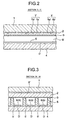
- Figs. 1 to 3 show a part of a conventional structure of alternating-current plasma display panel of surface discharge type. See Japanese Patent Kokai No. 5-205642 (Patent Document 1), for example.
- the plasma display panel is formed with a structure for causing discharge on each pixel between the parallel-arranged front glass substrate 1 and back glass substrate 4, as shown in Fig. 2.
- the front glass substrate 1 has a surface to serve as a display surface.
- the front glass substrate 1 has a back surface, on which provided are a plurality of elongate electrode pairs (X', Y'), a dielectric layer 2 covering the row electrode pairs (X', Y'), and a protection layer 3 of MgO (magnesium oxide) covering a back surface of the dielectric layer 2, in the order.
- MgO magnesium oxide
- Each row electrode X', Y' is structured by a transparent electrode Xa', Ya' made by a wide transparent conductive film of ITO or the like and a bus electrode Xb', Yb' made by a narrow metal film compensating for a conductivity thereof.
- the row electrodes X' and Y' are alternately arranged vertically on the display screen such that they are opposed at respective sides, to form a discharge gap g'.
- the row electrode pair (X', Y') constitutes one display line (row) L for matrix display.
- a discharge space S' exists where an Ne-Xe gas containing xenon is filled, as shown in Fig. 2.
- a discharge cell C' as a light-emitting unit area that the discharge space S' is demarcated at the intersection of the column electrode D' and the row electrode pair (X', Y'), as shown in Fig. 1.
- the period of one-field display is divided into N sub-fields, to assign each of the sub-fields with the number of times of light emissions corresponding to the weighting of that sub-field.
- the discharge cell is set with a sub-field for light emission and a sub-field not for light emission, thus driven to emit light.
- perception is at intermediate luminance in compliance with the total number of times of light generations throughout one of the fields.
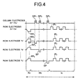
- Fig. 4 shows various driving pulses to be applied to the PDP within each sub-field, for realizing the foregoing driving.
- the sub-field is constituted by a simultaneous reset period Rc, an address period Wc and a sustain period Ic.
- reset pulses RPx, RPy are simultaneously applied to between the row electrode X 1 ' - X n ' and Y 1 ' - Y n ' which respectively form pairs, thereby simultaneously causing reset discharge in all the discharge cells. This once forms a predetermined amount of wall charge in each discharge cell.
- a scanning pulse SP is applied to the row electrodes Y 1 ' - Y n ' in the order, and a pixel data pulse based on each pixel corresponding to the input video signal is applied in an amount of one display line per time to the column electrodes D 1 ' - D m '. Namely, as shown in Fig.
- the column electrodes D 1 ' - D m ' are sequentially applied respectively by the pixel data pulse groups DP 1 - DP n each comprising pixel data pulses in the number of m and corresponding to the first to the n-th display line, synchronously with the scanning pulse SP.
- address discharge selective erase discharge
- the wall charge formed within the discharge cell is vanished away. Meanwhile, within the discharge cell where address discharge is not caused, the wall charge remains.
- sustain pulses IPx, IPy are applied in the number corresponding to a weighting on each sub-field to between the mating row electrodes X 1 ' - X n ' and Y 1 ' - Y n '.
- a vacuum ultraviolet ray having a wavelength 147 nm is emitted from the xenon Xe filled within the discharge space S'.
- the vacuum ultraviolet ray excites the red (R), green (G) and blue (B) fluorescent layer formed on the back substrate, to generate a visible portion of light.
- the present invention has been made in order to solve the problem, and it is an object to provide a display device capable of preventing erroneous discharge and improving the quality of display.
- a display device of the present invention is a display device for carrying out an image display according to pixel data on each pixel on the basis of an input video signal, correspondingly to the input video signal, comprising: a display panel having front and back substrates arranged to sandwich a discharge space; a plurality of row electrode pairs provided on an inner surface of the front substrate; a plurality of column electrodes arranged crossing the row electrode pairs on the inner surface of the back substrate; and unit light-emitting areas, respectively formed at intersections of the row electrode pairs and the column electrodes, each comprising a first discharge cell and a second discharge cell having a light absorbing layer close to the front substrate and a secondary-electron emitting material layer close to the back substrate; an address means for sequentially applying, while sequentially applying a scanning pulse having a polarity for placing the column electrode in a low potential to first row electrodes of first and second row electrodes constituting the row electrode pairs, a pixel data pulse having a voltage corresponding to the pixel data in an amount of one display line per
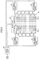
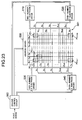
- Fig. 5 shows a configuration of a plasma display as a display device according to the present invention.
- the plasma display device is configured with a PDP 50 as a plasma display panel, an odd-number X electrode driver 51, an even-number X electrode driver 52, an odd-number Y electrode driver 53, an even-number Y electrode driver 54, an address driver 55 and a drive control circuit 56.
- the PDP 50 is formed thereon with strip-formed column electrodes D 1 - D m extending vertically on a display screen. Furthermore, the PDP 50 is formed thereon with strip-formed row electrodes X 1 - X n and row electrodes Y 2 - Y n extending horizontally on the display screen, which are alternately arranged in the numerical order as shown in Fig. 5.
- the row electrodes in a pair i.e. row electrode pair (X 2 , Y 2 ) - row electrode pair (X n , Y n ), serve as a first to (n - 1)-th display line on the PDP 50.
- Pixel cells PC serving as pixels, are respectively formed at intersections of the display lines and the column electrodes D 1 - D m (in areas surrounded by the one-dot chain line in Fig. 5). Namely, on the PDP 50, arranged are pixel cells PC 1.1 - PC 1,m belonging to the first display line, pixel cells PC 2.1 - PC 2,m belonging to the second display line, ... , pixel cells PC n- 1.1 - PC n-1,m belonging to the (n - 1)-th display line, in a matrix form.
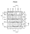
- Figs. 6 to 9 show a part of internal structure of the PDP 50 by excerption.
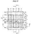
- Fig. 6 is a plan view of the PDP 50 as viewed from the front.
- Fig. 7 is a sectional view of the PDP 50 as viewed from the line V1-V1 shown in Fig. 6.
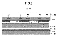
- Fig. 8 is a sectional view of the PDP 50 as viewed from the line V2-V2 shown in Fig. 6.
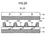
- Fig. 9 is a sectional view of the PDP 50 as viewed from the line W1-W1 shown in Fig. 6.
- the row electrode Y is structured by a strip-formed bus electrode Yb (row electrode Y main body) extending horizontally on the display screen and a plurality of transparent electrodes Ya connected to the bus electrode Yb.
- the bus electrode Yb is formed by a metal film, e.g. in black.
- the transparent electrodes Ya are made by a transparent conductive film of ITO or the like, and respectively arranged in positions corresponding to the column electrodes D on the bus electrode Yb.
- the transparent electrode Ya extends in a direction orthogonal to the bus electrode Yb, whose one and the other ends formed wide as shown in Fig. 6. Namely, the transparent electrode Ya can be considered as a projection electrode projecting from the main body of the row electrode Y.
- the row electrode X is structured by a strip-formed bus electrode Xb (row electrode X main body) extending horizontally on the display screen and a plurality of transparent electrodes Xa connected to the bus electrode Xb.
- the bus electrode Xb is formed by a metal film, e.g. in black.
- the transparent electrodes Xa are made by a transparent conductive film of ITO or the like, and respectively arranged in positions corresponding to the column electrodes D on the bus electrode Xb.
- the transparent electrode Xa extends in a direction orthogonal to the bus electrode Xb, whose one end is formed wide as shown in Fig. 6. Namely, the transparent electrode Xa can be considered as a projection electrode projecting from the main body of the row electrode X.
- the wide parts of the transparent electrodes Xa and Ya are arranged opposite to each other through a predetermined width of discharge gap g, as shown in Fig. 6.
- the row electrodes X and Y in pair have transparent electrodes Xa and Ya, as projection electrodes projecting from the main bodies thereof, which are oppositely arranged through the discharge gap g.
- the row electrode Y made by a transparent electrode Ya and bus electrode Yb and the row electrode X made by a transparent electrode Xa and bus electrode Xb are formed on a back surface of a front glass substrate 10 to serve as a display surface of PDP 50, as shown in Fig. 7. Furthermore, a dielectric layer 11 is formed on the back surface of the front glass substrate 10 in order to cover the row electrodes X and Y. In the corresponding positions to control discharge cells C2 (referred later) on a surface of the dielectric layer 11, a bulking dielectric layer 12 is formed projecting from the dielectric layer 11 toward the back.
- the bulking dielectric layer 12 is made by a light absorbing layer in a strip form containing a black or dark-color pigment, and formed extending horizontally on the display surface as shown in Fig. 6.
- the surface of the bulking dielectric layer 12 and of the dielectric layer 11 where the bulking dielectric layer 12 is not formed is covered by a protection layer (not shown) of MgO (magnesium oxide).
- MgO manganesium oxide
- a white column-electrode protection layer (dielectric layer) 14 is formed covering the column electrodes D.
- a division wall 15 is formed by a first lateral wall 15A, a second lateral wall 15B and a longitudinal wall 15C.
- the first lateral wall 15A is formed extending horizontally on the display surface, in a position opposite to the bus electrode Yb on the column-electrode protection layer 14.
- the second lateral wall 15B is formed extending horizontally on the display surface, in a position opposite to the bus electrode Xb on the column-electrode protection layer 14.
- the longitudinal wall 15C is formed extending orthogonally to the bus electrode Xb (Yb), in a position between the transparent electrode Xa (Ya) arranged with the equal gap.
- a secondary-electron emitting material layer 30 is formed on the column electrode protection layer 14, in an area opposed to the bulking dielectric layer 12 (including the side faces of the longitudinal wall 15c, first lateral wall 15A and second lateral wall 15B).
- the secondary-electron emitting material layer 30 is a layer formed of a high ⁇ material having a high work function (e.g. at 4.2 eV or lower), high in what is called secondary-electron emitting coefficient.
- the material usable for the secondary-electron emitting material layer 30 includes alkali earth metal oxide such as MgO, CaO, SrO and BaO, alkali metal oxide such as Cs 2 O, fluoride such as CaF 2 and MgF 2 , TiO 2 , Y 2 O 3 or a material enhanced in secondary-electron emitting coefficient by crystal defects or impurity doping, diamond-like thin film, carbon nano-tube, and so on.
- a fluorescent layer 16 is formed on the column-electrode protection layer 14, in the area other than the area opposed to the bulking dielectric layer 12 (including the side faces of the longitudinal wall 15c, first lateral wall 15A and second lateral wall 15B).
- the fluorescent layer 16 includes a red fluorescent layer for causing red light, a green fluorescent layer for causing green light, and a blue fluorescent layer for causing blue light. These are determined in assignment based on each pixel cell PC.
- the first lateral wall 15A, second lateral wall 15B and longitudinal wall 15C have a height not so high as reaching a surface of the bulking dielectric layer 12 or dielectric layer 11, as shown in Figs. 7 and 9. Consequently, a gap r exists allowing a discharge gas to pass between the second lateral wall 15B and the bulking dielectric layer 12, as shown in Fig. 7.
- a dielectric layer 17 is formed extending in a direction along the first lateral wall 15A, in order to prevent discharge interference. Also, between the longitudinal wall 15C and the bulking dielectric layer 12, a dielectric layer 18 is formed intermittently in a direction along the longitudinal wall 15C, as shown in Fig. 8.
- the area surrounded by the first lateral wall 15A and the longitudinal wall 15C provides a pixel cell PC to serve as a pixel. Furthermore, as shown in Figs. 6 and 7, the pixel cell PC is divided by the second lateral wall 15B, into a display discharge cell C1 and a control discharge cell C2.
- the display discharge cell C1 includes a pair of row electrodes X and Y serving as a display line and a fluorescent layer 16, as shown in Figs. 6 and 7.
- the control discharge cell C2 includes a row electrode Y of the row electrodes in one pair serving as the display line, a row electrode X of the row electrodes in one pair serving as the display line above adjacent to the display line on the display surface, a bulk dielectric layer 12 and a secondary-electron emitting material layer 30.
- the display discharge cell C1 there are oppositely arranged a wide part formed at one end of the transparent electrode Xa of the row electrode X and a wide part formed at one end of the transparent electrode Ya of the row electrode Y through a discharge gap g, as shown in Fig. 6.
- the control discharge cell C2 there is included a wide part formed at the other end of the transparent electrode Ya but not included a transparent electrode X.
- the pixel cells PC vertically adjacent on the display surface are shielded in their discharge spaces by the first lateral wall 15A and dielectric layer 17.
- the display discharge cell C1 and the control discharge cell C2, belonging to the same pixel cell PC are communicated with each other in discharge space through the gap r, as shown in Fig. 7.
- the control discharge cells C2 mutually adjacent in the left-right direction on the display surface are shielded in their discharge spaces by the bulking dielectric layer 12 and dielectric layer 18, as shown in Fig. 8, whereas the display discharge cells C1 mutually adjacent in the left-right direction on the display surface are communicated in their discharge spaces with each other.
- the pixel cell PC 1.1 - PC n-1,m formed on the PDP 50 is structured by a display discharge cell C1 and a control discharge cell C2 having respective discharge spaces communicated with each other.
- the odd-number X electrode driver 51 applies various drive pulses (referred later) to the odd-numbered (shown in Fig. 5) row electrodes X 1 , X 3 , X 5 , ..., X n-2 and X n of the row electrodes X of the PDP 50, according to a timing signal supplied from the drive control circuit 56.
- the even-number X electrode driver 52 applies various drive pulses (referred later) to the even-numbered (shown in Fig. 5) row electrodes X 2 , X 4 , X 6 , ..., X n-3 and X n-1 of the row electrodes X of the PDP 50, according to a timing signal supplied from the drive control circuit 56.
- the odd-number Y electrode driver 53 applies various drive pulses (referred later) to the odd-numbered (shown in Fig. 5) row electrodes Y 3 , Y 5 , ..., Y n-2 and Y n of the row electrodes Y of the PDP 50, according to a timing signal supplied from the drive control circuit 56.
- the even-number Y electrode driver 54 applies various drive pulses (referred later) to the even-numbered (shown in Fig. 5) row electrodes Y 2 , Y 4 , ..., Y n-3 and Y n-1 of the row electrodes Y of the PDP 50, according to a timing signal supplied from the drive control circuit 56.
- the address driver 55 applies a pixel data pulse (referred later) to the column electrodes D 1 - D m of the PDP 50, according to a timing signal supplied from the drive control circuit 56.
- the drive control circuit 56 first converts an input video signal into, for example, 8-bit pixel data representative of a luminance level on each pixel, and carries out error-diffusion process and dither process on the pixel data. For example, in the error-diffusion process, at first pixel data is taken higher 6 bits as display data and the remaining lower 2 bits as error data. The weighted addition of error data on the relevant pixel data corresponding to each of peripheral pixels is reflected in the display data. By this operation, the luminance of lower 2 bits on an original pixel is artificially expressed by the peripheral pixels. Accordingly, by 6-bit image data less than 8 bits, luminance tonal representation is made available equivalent to that of 8-bit pixel data.
- Dither process is carried out on the 6-bit error-diffusion-processed pixel data.
- a plurality of mutually adjacent pixels are taken as one pixel unit, so that dither coefficients of mutually different coefficient values are respectively assigned in those of error-diffusion-processed pixel data corresponding to the pixels of one pixel unit and added together, thereby obtaining dither-addition pixel data.
- the dither-addition pixel data only in higher 4 bits can express a luminance corresponding to that of 8 bits.
- the drive control circuit 56 takes the higher four bits of dither-addition pixel data as multi-gradation pixel data PDs.
- This is converted into 15-bit pixel drive data GD comprising the 1st to 15th bits, according to a data conversion table as shown in Fig. 10.
- the pixel data for representing 256 tonal levels on 8 bits is converted into 15-bit pixel drive data GD comprising 16 patterns in total, as shown in Fig. 10.
- the drive control circuit 56 separates these of pixel drive data GD 1.1 - GD (n-1),m between the same bit figures, based on one screen of pixel drive data GD 1.1 - GD (n-1),m .
- pixel-drive data bit groups DB1 - DB15 are obtained as follows:
- the pixel-driving data bit groups DB1 - DB15 correspond respectively to sub-fields SF1 - SF15, referred later.
- the drive control circuit 56 in each sub-field SF1 - SF15, supplies a pixel-driving data bit group DB corresponding to the sub-field in an amount of one display line (m in the number) per time to the address driver 55.
- the drive control circuit 56 generates various timing signals to control the drive to the PDP 50, according to a light-emitting drive sequence as shown in Fig. 11, and supplies those to the odd-number X electrode driver 51, the even-number X electrode driver 52, the odd-number Y electrode driver 53 and the even-number Y electrode driver 54.
- each field of video signal is divided into fifteen sub-fields SF1 - SF15, to execute an address process W, light-emission maintaining process I and erase process E in each sub-field.
- a simultaneous reset process R is executed in advance of the address process W.
- Fig. 12 shows the various drive pulses to be applied in the simultaneous reset process R, address process W, light-emission maintaining process I and erase process E by the odd-number X electrode driver 51, even-number X electrode driver 52, odd-number Y electrode driver 53 and even-number Y electrode driver 54 to the PDP 50.
- Fig. 12 shows only the head sub-field SF1 by excerption.
- the odd-number X electrode driver 51 and even-number X electrode driver 52 generate negative-polarity reset pulses RP x moderate in fall change as compared to the sustain pulse (referred later), and apply them simultaneously to the row electrodes X 1 - X n of the PDP 50.
- the odd-number Y electrode driver 53 and even-number Y electrode driver 54 generate negative-polarity reset pulses RP Y moderate in fall change as compared to the sustain pulse (referred later), and apply them simultaneously to the row electrodes Y 2 - Y n of the PDP 50.
- the address driver 55 generates positive-polarity reset pulses RP D and applies them simultaneously to the column electrodes D 1 - D n of the PDP 50.
- reset discharge (erase discharge) is caused within each control discharge cell C2 of the pixel cell PC 1.1 - PC( n-1),m of the PDP 50.
- the column electrode D end is to act as anode relative to the row electrodes X, Y.
- wall charge existing within the control discharge cell C2 in every pixel cell PC is vanished away.
- the odd-number Y electrode driver 53 and even-number Y electrode driver 54 apply a scanning pulse SP having a positive-polarity voltage V2 (V2 > V1) sequentially to the row electrodes Y 2 - Y n while applying a positive-polarity voltage V1 to all the row electrodes Y 2 - Y n .
- the address driver 55 converts the data bits in the pixel-driving data bit group DB1 corresponding to this sub-field SF1 into a pixel data pulse DP having a pulse voltage commensurate with the logic level thereof.
- the address driver 55 converts, on one hand, a pixel-driving data bit having logic level 0 into a positive-polarity high voltage pixel data, and, on the other hand, a pixel-driving data bit having logic level 1 into a low-voltage (0 volt) pixel data pulse DP.
- a pixel data pulse DP is applied in an amount of one display line (m in the number) per time to the column electrode D 1 - D m , synchronously with application timing of the scanning pulse SP.
- the address driver 55 first applies the column electrode D 1 - D m with a pixel data pulse group DP 1 comprising pixel data pulses DP in the number of m corresponding to the first display line, and then the column electrode D 1 - D m with a pixel data pulse group DP 2 comprising pixel data pulses DP in the number of m corresponding to the second display line.
- write address discharge is caused between the column electrode D and the row electrode Y within the control discharge cell C2 of the pixel cell PC to which is applied a low-voltage (0 volt) pixel data pulse DP together with a scanning pulse SP having a positive-polarity voltage V2.
- write address discharge is selectively caused in the control discharge cell C2 of each pixel cell PC according to the data bit of pixel-driving data bit group corresponding to the sub-field, thereby forming wall charge.
- the pixel cell PC formed with wall charge is set to light on-cell mode while the pixel cell PC not formed with wall charge is set to light-off cell mode.
- the odd-number Y electrode driver 53 repeats a positive-polarity sustain pulse IP YO the number of times assigned in the sub-field to which the sustain process I belongs, to apply them to the odd-numbered row electrodes Y 3 , Y 5 , ..., Y n .
- the even-number X electrode driver 52 repeats a positive-polarity sustain pulse IP XE the number of times assigned in the sub-field to which the sustain process I belongs, to apply them to the even-numbered row electrodes X 2 , X 4 , ..., X n-1 .
- the odd-number X electrode driver 51 repeats a positive-polarity sustain pulse IP XO the number of times assigned in the sub-field to which the sustain process I belongs, to apply them to the odd-numbered row electrodes X 1 , X 3 , X 5 , ...., X n .
- the even-number Y electrode driver 54 repeats a positive-polarity sustain pulse IP YE the number of times assigned in the sub-field to which the sustain process I belongs, to apply them to the even-numbered row electrodes Y 2 , Y 4 , ..., Y n-1 ⁇
- the sustain pulse IP XE or IP YO and the sustain pulse IP XO and IP YE are deviated in application timing from each other, as shown in Fig. 12.
- sustain discharge is caused between the transparent electrodes Xa and Ya within the display discharge cell C1 of the pixel cell PC set in the light on-cell mode.
- the fluorescent layer 16 red, green or blue florescent layer formed in the display discharge cell C1, as shown in Fig. 7.
- the light corresponding to the fluorescent color is radiated through the front glass substrate 10. Namely, light emission is repeatedly caused by sustain discharge the number of times assigned in the sub-field to which the sustain process I belongs.
- the odd-number X electrode driver 51 and even-number X electrode driver 52 apply a positive-polarity erase pulse EP x as shown in Fig. 12 to all the row electrodes X. Furthermore, the odd-number Y electrode driver 53 and even-number Y electrode driver 54 apply a positive-polarity erase pulse EP Y as shown in Fig. 12 to all the row electrodes Y.
- EP x and EP Y erase discharge is caused between the row electrode Y and the column electrode D within every control discharge cell C2 and between the row electrodes X and Y within every display discharge cell C1. This erases the wall charge remained within every pixel cell PC.
- the driving by the simultaneous reset process R, address process W, light-emission maintaining process I and erase process E is executed on the basis of the pixel-driving data GD in 16 combinations as shown in Fig. 10.
- write address discharge (shown by the double circle in Fig 10) is caused in the address process W in each of sub-fields in an amount corresponding to an intermediate luminance to express.
- the pixel cells PC are set to light on-cell mode in each of the sub-fields continuing in an amount corresponding to the intermediate luminance to express.
- Light emission is caused by sustain discharge repeatedly the number of times assigned in each of the sub-fields. On this occasion, perceived is a luminance corresponding to the total number of times of light emissions due to sustain discharge caused within one field.
- the pixel cell PC serving as a pixel for the PDP 50 is configured by a display discharge cell C1 and a control discharge cell C2, as shown in Figs. 6 and 7.
- Sustain discharge related to a display image is caused within the display discharge cell C1 while reset and address discharges with light emission not related to a display image is caused mainly within the control discharge cell C2.
- a bulking dielectric layer 12 is formed comprising a light-absorbing layer containing a black or dark-color pigment in order to prevent the light caused by reset and address discharges from leaking outside through the front glass substrate 10. Accordingly, because the discharge light due to reset and address discharges is cut off by the bulking dielectric layer 12, contrast, particularly dark contrast, can be enhanced on the display image.
- a secondary-electron emitting material layer 30 is provided on a side close to the back substrate 13, as shown in Fig. 7.
- the secondary-electron emitting material layer 30 has a ⁇ characteristic for emitting secondary electrons given favorable upon discharge wherein the forming surface thereof acts as a cathode.
- a scanning pulse SP having a positive-polarity voltage V2 is applied to the row electrode Y while a low-voltage (0 volt) pixel data pulse DP is applied to the column electrode D.
- the column electrode D is rendered as a cathode end during write address discharge. Consequently, the secondary-electron emitting material layer 30 formed within the control discharge cell C2 also acts as a cathode. Secondary electrons are to be favorably emitted from the secondary-electron emitting material layer 30. Accordingly, write address discharge is positively caused within the control discharge cell C2.
- the drive control circuit 56 When carrying out driving on a selective erase address method, the drive control circuit 56 first converts an input video signal into 8-bit pixel data representative of a luminance level on each pixel, and carries out error-diffusion process and dither process on the pixel data. By the error-diffusion process and dither process, the drive control circuit 56 converts the 8-bit pixel data into 4-bit multi-gradation pixel data PD s , and further converts the multi-gradation pixel data PD s into 15-bit pixel drive data GD according to a data conversion table shown in Fig. 13. Due to this, the pixel data capable of representing 256 tonal levels on 8 bits is converted into 15-bit pixel drive data GD comprising 16 patterns in total.
- the drive control circuit 56 separates these of pixel drive data GD 1.1 - GD (n-1),m between the same bit figures, based on one screen of pixel drive data GD 1.1 - GD (n-1),m , thus obtaining pixel-drive data bit groups DB1 - DB15.
- the drive control circuit 56 supplies, based on each sub-field SF1 - SF15, a pixel-driving data bit group DB corresponding to the sub-field in an amount of one display line (m in the number) per time to the address driver 55.
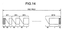
- Fig. 14 shows a light-emission driving sequence upon tonally driving the PDP 50 by applying a selective erase address scheme.
- the field of video signal is divided into fifteen sub-fields SF1 - SF15, to carry out address process W and light-emission maintaining process I in each of the sub-fields.
- simultaneous reset process R is executed in advance of the address process W.
- erase process E is executed immediately after the light-emission maintaining process I.
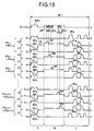
- Fig. 15 shows the various drive pulses which the odd-number X electrode driver 51, even-number X electrode driver 52, odd-number Y electrode driver 53 and even-number Y electrode driver 54 apply to the PDP 50 in the simultaneous reset process R, address process W, and light-emission maintaining process I, according to the light-emission driving sequence shown in Fig. 14.
- Fig. 15 shows only the head sub-field SF1 by excerption.
- the odd-number Y electrode driver 53 and even-number Y electrode driver 54 generate negative-polarity reset pulses RP Y moderate in fall change as compared to the sustain pulse (referred later), and apply them simultaneously to the row electrodes Y 2 - Y n of the PDP 50.
- the odd-number X electrode driver 51 and even-number X electrode driver 52 generate positive-polarity reset pulses RP X and apply them simultaneously to the row electrodes X 1 - X n of the PDP 50.
- the address driver 55 generates positive-polarity reset pulses RP D and applies them simultaneously to the column electrodes D 1 - D n of the PDP 50.
- reset discharge (write discharge) is caused between the column electrode D and the row electrode Y within the control discharge cell C2 of every pixel cell PC of the PDP 50, thereby forming wall charge within the control discharge cell C2.
- the column electrode D end is to act as anode relative to the row electrodes X, Y.
- the reset discharge moves toward the display discharge cell C1 through the gap r as shown in Fig. 7, to cause a discharge between the row electrodes Y and X within the display discharge cell C1.
- on-wall discharge is formed within the display discharge cell C1 of every pixel cell PC.
- wall charge is formed within the display discharge cell C1 of every pixel cell PC of the PDP 50, thus initializing all the pixel cells PC into light on-cell mode.
- the odd-number Y electrode driver 53 and even-number Y electrode driver 54 apply a scanning pulse SP having a positive-polarity voltage V2 (V2 > V1) sequentially to the row electrodes Y 2 - Y n while applying a positive-polarity voltage V1 to all the row electrodes Y 2 - Y n .
- the address driver 55 converts the data bits in the pixel-driving data bit group DB1 corresponding to this sub-field SF1 into a pixel data pulse DP having a pulse voltage commensurate with the logic level thereof.
- the address driver 55 converts, on one hand, a pixel-driving data bit having logic level 0 into a positive-polarity high voltage pixel data pulse DP, and, on the other hand, a pixel-driving data bit having logic level 1 into a low-voltage (0 volt) pixel data pulse DP.
- a pixel data pulse DP is applied in an amount of one display line (m in the number) per time to the column electrode D 1 - D m , synchronously with application timing of the scanning pulse SP.
- the address driver 55 first applies the column electrode D 1 - D m with a pixel data pulse group DP 1 comprising pixel data pulses DP in the number of m corresponding to the first display line, and then the column electrode D 1 - D m with a pixel data pulse group DP 2 comprising pixel data pulses DP in the number of m corresponding to the second display line.
- erase address discharge is caused between the column electrode D and the row electrode Y within the control discharge cell C2 of the pixel cell PC to which is applied a low-voltage (0 volt) pixel data pulse DP together with a scanning pulse SP having a positive-polarity voltage V2.
- erase address discharge is selectively caused in the control discharge cell C2 of pixel cell PC according to the data bits of pixel-driving data bit group corresponding to the sub-field, thereby erasing wall charge. Due to this, the pixel cell PC where wall charge remains is set to light on-cell mode while the pixel cell PC where wall charge is erased is set to light-off cell mode.
- the odd-number Y electrode driver 53 repeats a positive-polarity sustain pulse IP YO the number of times assigned in the sub-field to which the sustain process I belongs, to apply them to the odd-numbered row electrodes Y 3 , Y 5 , ..., Y n .
- the even-number X electrode driver 52 repeats a positive-polarity sustain pulse IP XE the number of times assigned in the sub-field to which the sustain process I belongs, to apply them to the even-numbered row electrodes X 2 , X 4 , ..., X n-1 .
- the odd-number X electrode driver 51 repeats a positive-polarity sustain pulse IP XO the number of times assigned in the sub-field to which the sustain process I belongs, to apply them to the odd-numbered row electrodes X 1 , X 3 , X 5 , ..., X n .
- the even-number Y electrode driver 54 repeats a positive-polarity sustain pulse IP YE the number of times assigned in the sub-field to which the sustain process I belongs, to apply them to the even-numbered row electrodes Y 2 , Y 4 , ..., Y n-1 .
- the sustain pulses IP XE and IP YO and the sustain pulses IP XO and IP YE are deviated in application timing from each other, as shown in Fig. 15.
- sustain pulse IP XO , IP XE , IP YO or IP YE is applied, sustain discharge is caused between the transparent electrodes Xa and Ya within the display discharge cell C1 of the pixel cell PC set in the light on-cell mode.
- the fluorescent layer 16 red, green or blue florescent layer formed in the display discharge cell C1, as shown in Fig. 7.
- the light corresponding to the fluorescent color is radiated through the front glass substrate 10. Namely, light emission repeatedly occurs due to sustain discharge the number of times assigned in the sub-field to which the sustain process I belongs.
- the driving based on the simultaneous reset process R, address process W, and light-emission maintaining process is executed on the basis of the pixel-driving data GD in 16 combinations as shown in Fig. 13.
- the pixel cell PC can be transited from light-off cell mode to light on-cell mode only on the occasion of simultaneous reset process R in the sub-field SF1. Consequently, erase address discharge is caused in one sub-field of the sub-fields SF1 - SF15.
- this pixel cell PC does not return to light on-cell mode in the subsequent sub-field.
- pixel cell PC is set to light on-cell mode in the sub-field continuing in an amount corresponding to a luminance to express. Until erase address discharge (shown by black circle) is caused, sustain discharge emission of light (shown by white circle) is carried out continuously in the sustain process I of each sub-field.
- a scanning pulse SP having a positive-polarity voltage V2 is applied to the row electrode Y while a low-voltage (0 volt) pixel data pulse DP is applied to the column electrode D.
- the secondary-electron emitting material layer 30 formed in the control discharge cell C2 is to act as a cathode relative to the row electrode Y. Accordingly, when causing erase address discharge, secondary electrons are favorably emitted from the secondary-electron emitting material layer 30, thus positively causing erase address discharge within the control discharge cell C2.
- Fig. 16 shows a configuration of a plasma display device mounting a display panel having row electrodes X and Y in an arrangement of X, X, Y, Y, X, X, Y, Y.
- the plasma display device employs a PDP 500 having row electrodes X and Y in an arrangement order of X, X, Y, Y, X, X, Y, Y, in place of the PDP 50 shown in Fig. 5.
- the other structure is the same as that shown in Fig. 5.
- the PDP 500 is formed with strip-formed column electrodes D 1 - D m extending vertically on the display screen. Furthermore, the PDP 500 is formed with strip-formed row electrodes X 1 - X n and row electrodes Y 2 - Y n extending horizontally on the display screen, which are arranged alternately in the numerical order.
- the electrodes in a pair i.e. row electrode pair (X 2 , Y 2 ) - row electrode pair (X n , Y n ), are to respectively act as the first to (n - 1)-th display lines of the PDP 500.
- Pixel cells PC are respectively formed at intersections between the display lines and the column electrodes D 1 - D m (in areas surrounded by the one-dot chain line in Fig. 16).
- the PDP 500 is arranged with pixel cells PC 1.1 - PC 1,m belonging to the first display line, pixel cells PC 2.1 - PC 2,m belonging to the second display line, ... , pixel cells PC n- 1.1 - PC n-1,m belonging to the (n - 1)-th display line, in a matrix form.
- Figs. 17 to 20 show a part of internal structure of the PDP 500 by excerption.
- Fig. 17 is a plan view showing a structure as viewed from the front.
- Fig. 18 is a sectional view as viewed from the line V1-V1 shown in Fig. 17.
- Fig. 19 is a sectional view as viewed from the line V2-V2.
- Fig. 20 is a sectional view as viewed from the line W1-W1 shown in Fig. 17.
- the structural elements denoted by the same numerals as those shown in Figs. 6 to 9 are the same ones.
- the PDP 500 is formed thereon with pixel cells PC each comprising a pair of discharge cells (display discharge cell C1 and control discharge cell C2) having the same structure as that of the PDP 50, in a matrix form. It is noted that the PDP 500 has control discharge cells C2 arranged respectively of the two pixel cells mutually adjacent vertically on the screen, differently from the PDP 50.
- the adjacent control discharge cells C2 are shielded in discharge space by a first lateral wall 15A and dielectric layer 17, as shown in Fig. 18.
- Fig. 21 shows the various drive pulses to be applied to the PDP 500 by the odd-number X electrode driver 51, even-number X electrode driver 52, odd-number Y electrode driver 53 and even-number Y electrode driver 54 when driving the PDP 500 according to a driving sequence as shown in Figs. 10 and 11 adopting a selective write address scheme.
- the reset pulse RP x , RP y , RP D , pixel data pulse DP, scanning pulse SP, sustain pulse IP XO , IP XE , IP YE , IP YO , erase pulses EP x and EP y to be applied in a simultaneous reset process R, address process W, sustain process I or erase process E are the same as those shown in Fig. 12. Namely, the discharge to be caused by applying those drive pulses and the operation based on the discharge are the same as those explained in Fig. 12. It is noted that, in the driving shown in Fig.
- sustain pulses IP XO and IP XE are applied in the same timing to all the row electrodes X in the sustain process I, and further sustain pulses IP YE and IP YO are applied in the timing different from the IP XO and IP XE to all the row electrodes Y.
- Fig. 22 shows the various drive pulses to be applied to the PDP 500 by the odd-number X electrode driver 51, even-number X electrode driver 52, odd-number Y electrode driver 53 and even-number Y electrode driver 54 when driving the PDP 500 according to a driving sequence as shown in Figs. 13 and 14 adopting a selective erase address scheme.
- the reset pulse RP x , RP y , RP D , pixel data pulse DP, scanning pulse SP, sustain pulse IP XO , IP XE , IP YE and IP YO to be applied in the simultaneous reset process R, address process W and sustain process I are the same as those shown in Fig. 15. Namely, the discharge to be caused by applying those drive pulses and the operation based on the discharge are the same as those explained in Fig. 15. It is noted that, in the driving shown in Fig.
- sustain pulses IP XO and IP XE are applied in the same timing to all the row electrodes X in the sustain process I, and further sustain pulses IP YE and IP YO are applied in the timing different from the IP XO and IP XE to all the row electrodes Y.
- Fig. 23 shows another configuration of a plasma display as a display device.
- the plasma display is configured with a PDP 501 as a plasma display panel, an odd-number X electrode driver 510, an even-number X electrode driver 520, an odd-number Y electrode driver 530, an even-number Y electrode driver 540, an address driver 550 and a drive control circuit 560.
- the PDP 501 is formed with strip-formed column electrodes D 1 - D m extending vertically on the display screen. Furthermore, the PDP 501 is formed with strip-formed row electrodes X 2 - X n and column electrodes Y 1 - Y n extending horizontally on the display screen, which are arranged alternately in the numerical order as shown in Fig. 23.
- the row electrodes in pair i.e. row electrode pair (X 2 , Y 2 ) - row electrode pair (X n , Y n ), are respectively to act as the first to (n - 1)-th display lines on the PDP 501.
- Pixel cells PC are respectively formed at intersections between the display lines and the column electrodes D 1 - D m (in areas surrounded by the one-dot chain line in Fig. 23).
- the PDP 501 is arranged with pixel cells PC 1.1 - PC 1,m belonging to the first display line, pixel cells PC 2.1 - PC 2,m belonging to the second display line, ... , pixel cells PC n-1.1 - PC n-1,m belonging to the (n - 1)-th display line, in a matrix form.
- Figs. 24 to 27 show a part of internal structure of the PDP 501 by excerption.
- Fig. 24 is a plan view of the PDP 501 as viewed from the front.
- Fig. 25 is a sectional view as viewed from the line V1-V1 shown in Fig. 24.
- Fig. 26 is a sectional view as viewed from the line V2-V2 shown in Fig. 24.
- Fig. 27 is a sectional view of the PDP 501 as viewed from the line W1-W1 shown in Fig. 24.
- the structural elements denoted by the same numerals as those shown in Figs. 6 to 9 are the same ones.
- the PDP 501 is arranged with pixel cells PC each comprising a pair of discharge cells (display discharge cell C1 and control discharge cell C2) having the same structure as that of the PDP 50, in a matrix form.
- the transparent electrode Xa serving as a row electrode X is formed with wide parts at both ends as shown in Fig. 24, differently from the PDP 50. Accordingly, a discharge gap g is also formed between the wide parts of the transparent electrodes Ya and Xa within the control discharge cell C2.
- the discharge gap g formed within the control discharge cell C2 is formed in a deviated position closer to the display discharge cell C1 which forms a pair with the relevant control discharge cell C2 than the intermediate point between the bus electrodes Xb and Yb formed within the control discharge cell C2.
- the odd-number X electrode driver 510 applies various drive pulses (referred later) to the odd-numbered (shown in Fig. 23) row electrodes X 3 , X 5 , ..., X n-2 and X n of the row electrodes X of the PDP 501, according to a timing signal supplied from the drive control circuit 560.
- the even-number X electrode driver 520 applies various drive pulses (referred later) to the even-numbered (shown in Fig. 23) row electrodes X 2 , X 4 , ..., X n-3 and X n-1 of the row electrodes X of the PDP 501, according to a timing signal supplied from the drive control circuit 560.
- the odd-number Y electrode driver 530 applies various drive pulses (referred later) to the odd-numbered (shown in Fig. 23) row electrodes Y 1 , Y 3 , Y 5 , ..., Y n-2 and Y n of the row electrodes Y of the PDP 501, according to a timing signal supplied from the drive control circuit 560.
- the even-number Y electrode driver 540 applies various drive pulses (referred later) to the even-numbered (shown in Fig. 23) row electrodes Y 2 , Y 4 , ..., Y n-3 and Y n-1 of the row electrodes Y of the PDP 501, according to a timing signal supplied from the drive control circuit 560.
- the address driver 550 applies a pixel data pulse (referred later) to the column electrodes D 1 - D m of the PDP 501, according to a timing signal supplied from the drive control circuit 560.
- the drive control circuit 560 first converts an input video signal into 8-bit pixel data representative of a luminance level on each pixel, and carries out error-diffusion process and dither process on the pixel data thereby obtaining 4-bit multi-gradation pixel data PD s . This is converted into 15-bit pixel driving data GD comprising first to fifteenth bit, according to a data converting table as shown in Fig. 28. Then, the drive control circuit 560 separates these of pixel drive data GD 1.1 - GD (n-1),m between the same bit figures, based on one screen of pixel drive data GD 1.1 - GD (n-1),m . Due to this, pixel-drive data bit groups DB1 - DB15 are obtained as follows:
- the pixel-driving data bit groups DB1 - DB15 correspond respectively to sub-fields SF1 - SF15, referred later.
- the drive control circuit 560 supplies, based on each sub-field SF1 - SF15, a pixel-driving data bit group DB corresponding to the relevant sub-field in an amount of one display line (m in the number) per time to the address driver 550.
- the drive control circuit 560 generates various timing signals for drive-controlling the PDP 501, according to a light-emitting drive sequence as shown in Fig. 29, and supplies those to the odd-number X electrode driver 510, the even-number X electrode driver 520, the odd-number Y electrode driver 530 and the even-number Y electrode driver 540.
- the field of video signal is divided into fifteen sub-fields SF1 - SF15, to execute the following driving process in each sub-field.
- Fig. 30 shows the various drive pulses to be applied to the PDP 501, in the sub-field SF1 shown in Fig. 29, by the odd-number X electrode driver 510, even-number X electrode driver 520, odd-number Y electrode driver 530, even-number Y electrode driver 540 and address driver 550, and application timing thereof.
- the odd-number Y electrode driver 530 At first, in the odd-numbered row reset process R OD , the odd-number Y electrode driver 530 generates positive-polarity first reset pulses RP Y1 moderate in rise change as compared to the sustain pulse (referred later), and applies them simultaneously to the odd-numbered row electrodes Y 1 , Y 3 , ..., Y n of the PDP 501.
- first reset discharge (write discharge) is caused between the row electrode Y and the column electrode D within the control discharge cell C2 of every pixel cell PC belonging to the odd-numbered display line.
- the odd-number Y electrode driver 530 subsequently generates negative-polarity second reset pulse RP Y2 and applies them simultaneously to the odd-numbered row electrodes Y 1 , Y 3 , ..., Y n of the PDP 501. Furthermore, in the same timing as the second reset pulse RP Y2 , the address driver 550 generates positive-polarity reset pulse RP D and applies them simultaneously to the row electrodes D 1 - D n .
- second reset discharge (erase discharge) is caused between the row electrode Y and the column electrode D within the control discharge cell C2 of each pixel cell PC belonging to the odd-numbered display line.
- negative and positive wall charges are respectively formed nearby the column electrode D and nearby the row electrode X and Y within the control discharge cell C2 of every pixel cell PC belonging to the odd-numbered display line.
- the odd-number Y electrode driver 530 applies a scanning pulse SP having a positive-polarity voltage V2 (V2 > V1) sequentially to the odd-numbered row electrodes Y 1 , Y 3 , Y 5 , ..., and Y n-2 while applying a positive-polarity voltage V1 to all the odd-numbered row electrodes Y.
- the address driver 550 converts the pixel-driving data bits corresponding to the odd-numbered display line in the pixel-driving data bit group DB1 corresponding to this sub-field SF1 into a pixel data pulse DP having a pulse voltage commensurate with the logic level thereof.
- the address driver 550 converts, on one hand, a pixel-driving data bit having logic level 0 into a positive-polarity high voltage pixel data pulse DP, and, on the other hand, a pixel-driving data bit having logic level 1 into a low-voltage (0 volt) pixel data pulse DP.
- the pixel data pulse DP is applied in an amount of one display line (m in the number) per time to the column electrodes D 1 - D m synchronously with application timing of the scanning pulse SP.
- the address driver 550 first applies the column electrodes D 1 - D m with a pixel data pulse group DP 1 comprising pixel data pulses DP in the number of m corresponding to the first display line, and then the column electrodes D 1 - D m with a pixel data pulse group DP 3 comprising pixel data pulses DP in the number of m corresponding to the third display line.
- write address discharge is selectively caused within the control discharge cell C2 of the pixel cell PC to which is applied a low-voltage (0 volt) pixel data pulse DP together with a scanning pulse SP having a positive-polarity voltage V2. Namely, write address discharge is caused between the column electrode D and the wide part of the transparent electrode Ya within the control discharge cell C2.
- the odd-number X electrode driver 510 continuously applies the odd-numbered row electrode X with a voltage in the same polarity as the scanning pulse SP, in order to prevent an erroneous discharge between the row electrode D and the column electrode X within the control discharge cell C2.
- the pixel cells PC corresponding to the odd-numbered display line are set to either temporary light on-cell mode or light-off cell mode according to the pixel data based on the input video signal.
- first reset discharge write discharge
- the even-number Y electrode driver 540 In the next even-numbered row reset process R EV , the even-number Y electrode driver 540 generates positive-polarity first reset pulses RP Y1 moderate in rise change as compared to the sustain pulse (referred later), and applies them simultaneously to the even-numbered row electrodes Y 2 , Y 4 , ... , Y n-1 of the PDP 501.
- first reset discharge write discharge
- the odd-number Y electrode driver 540 subsequently generates negative-polarity second reset pulse RP Y2 and applies them simultaneously to the even-numbered row electrodes Y 2 , Y 4 , ..., Y n-1 of the PDP 501. Furthermore, in the same timing as the second reset pulse RP Y2 , the address driver 550 generates positive-polarity reset pulse RP D and applies them simultaneously to the column electrodes D 1 - D n .
- second reset discharge (erase discharge) is caused between the row electrode Y and the column electrode D within the control discharge cell C2 of each pixel cell PC belonging to the even-numbered display line.
- negative and positive wall charges are respectively formed nearby the column electrode D and nearby the row electrode X and Y within the control discharge cell C2 of every pixel cell PC belonging to the even-numbered display line.
- the even-number Y electrode driver 540 applies a scanning pulse SP having a positive-polarity voltage V2 (V2 > V1) sequentially to the even-numbered row electrodes Y 2 , Y 4 , Y 6 , ..., Y n-1 while applying a positive-polarity voltage V1 to all the even-numbered row electrodes Y.
- the address driver 550 converts the pixel-driving data bits corresponding to the odd-numbered display line in the pixel-driving data bit group DB1 corresponding to this sub-field SF1 into a pixel data pulse DP having a pulse voltage commensurate with the logic level thereof.
- the address driver 550 converts, on one hand, a pixel-driving data bit having logic level 0 into a positive-polarity high voltage pixel data pulse DP, and, on the other hand, a pixel-driving data bit having logic level 1 into a low-voltage (0 volt) pixel data pulse DP.
- the pixel data pulse DP is applied in an amount of one display line (m in the number) per time to the column electrodes D 1 - D m synchronously with application timing of the scanning pulse SP.
- the address driver 550 first applies the column electrodes D 1 - D m with a pixel data pulse group DP 2 comprising pixel data pulses DP in the number of m corresponding to the second display line, and then the column electrodes D 1 - D m with a pixel data pulse group DP 4 comprising pixel data pulses DP in the number of m corresponding to the fourth display line.
- write address discharge is selectively caused within the control discharge cell C2 of the pixel cell PC to which is applied a low-voltage (0 volt) pixel data pulse DP together with a scanning pulse SP having a positive-polarity voltage V2.
- write address discharge is caused between the column electrode D and the wide part of the transparent electrode Ya within the control discharge cell C2.
- write address discharge as in the above is not caused.
- the even-number X electrode driver 520 continuously applies the odd-numbered row electrode X with a voltage in the same polarity as the scanning pulse SP, in order to prevent an erroneous discharge between the row electrode D and the column electrode X within the control discharge cell C2.
- the pixel cells PC corresponding to the even-numbered display line are set to either temporary light on-cell mode or light-off cell mode according to the pixel data based on an input video signal.
- the odd-number Y electrode driver 530 and even-number Y electrode driver 540 apply a positive-polarity scanning pulse SP as shown in Fig. 30 sequentially to the row electrodes Y 1 , Y 2 , Y 3 , ... Y n-1 (not shown).
- the address driver 550 converts the pixel-driving data bits in the pixel-driving data bit group DB(j) corresponding to each sub-field SF(j) [j is a natural number of 2 - 15] into a pixel data pulse DP having a pulse voltage commensurate with the logic level thereof.
- Such a pixel data pulse DP is applied in an amount of one display line (m in the number) per time to the column electrodes D 1 - D m , synchronously with application timing of the scanning pulse SP.
- write address discharge as noted before is selectively caused within the control discharge cell C2 of the pixel cell PC to which is applied a low-voltage (0 volt) pixel data pulse DP together with the scanning pulse SP.
- write address discharge as the above is not caused.
- the odd-number Y electrode driver 530 intermittently repeats a positive-polarity priming pulse PR YO as shown in Fig. 30, to apply them to the odd-numbered row electrodes Y 1 , Y 3 , ..., Y n .
- the odd-number X electrode driver 510 intermittently repeats a positive-polarity priming pulse PP XO in the same timing as the priming pulse PP YO , to apply them to the odd-numbered row electrodes X 3 , X 5 , ..., X n .
- the even-number X electrode driver 520 intermittently repeats a positive-polarity priming pulse PP XE in different timing from the above PP XO and PP YO as shown in Fig. 30, to apply them to the even-numbered row electrodes X 2 , X 4 , ..., X n-1 .
- the even-number Y electrode driver 540 intermittently repeats a positive-polarity priming pulse PP YE in the same timing as the priming pulse PP XE as shown in Fig. 30, to apply them to the even-numbered row electrodes Y 2 , Y 4 , ..., Y n-1 .
- priming discharge is caused between the transparent electrodes Xa and Ya within the control discharge cell C2 of the pixel cell PC set in the temporary light on-cell mode as noted before.
- discharge extends toward the display discharge cell C1 through the gap r as shown in Fig. 25, forming wall charge within the display discharge cell C1.
- priming discharge is caused repeatedly only in the control discharge cell C2 of the pixel cell PC set in temporary light on-cell mode in the odd-numbered row address process W OD , even-numbered row address process W EV or address process W, thereby gradually extending discharge toward the display discharge cell C1.
- Such an extension of the discharge forms wall charge within the display discharge cell C1.
- the pixel cell PC to which the display discharge cell C1 belongs is set to light on-cell mode.
- priming discharge is not caused. Accordingly, because wall charge is not formed within the display discharge cell C1 communicating with the relevant control discharge cell C2, the pixel cell C is set to light-off cell mode.
- the odd-number Y electrode driver 530 repeats a positive-polarity sustain pulse IP YO as shown in Fig. 30 the number of times assigned in the sub-field to which the sustain process I belongs, thereby applying them to the odd-numbered row electrodes Y 1 , Y 3 , Y 5 , ..., Y n .
- the even-number X electrode driver 520 generates a positive-polarity sustain pulse IP XE in the same timing as the sustain pulse IP YO and repeats it the number of times assigned in the sub-field the relevant sustain process I belongs, thereby applying them to the even-numbered row electrodes X 2 , X 4 , ..., X n-1 .
- the odd-number X electrode driver 510 generates a positive-polarity sustain pulse IP XO as shown in Fig. 30 in the different timing from the sustain pulse IP YO and repeats it the number of times assigned in the sub-field the relevant sustain process I belongs, thereby applying them to the odd-numbered row electrodes X 1 , X 3 , X 5 , ..., X n .
- the even-number Y electrode driver 540 generates a positive-polarity sustain pulse IP YE in the same timing as the sustain pulse IP XO and repeats it the number of times assigned in the sub-field the relevant sustain process I belongs, thereby applying them to the even-numbered row electrodes Y 2 , Y 4 , ..., Y n-1 .
- sustain pulse IP XO , IP XE , IP YO or IP YE is applied, sustain discharge is caused between the transparent electrodes Xa and Ya within the display discharge cell C1 of the pixel cell PC set in the light on-cell mode.
- the odd-number X electrode driver 51, even-number X electrode driver 52, odd-number Y electrode driver 53, even-number Y electrode driver 54 and address driver 55 apply a positive-polarity erase pulse EP to all the row electrodes X and Y.
- erase discharge is caused within every control discharge cell C2 where wall charge remains, thus erasing the wall charge.
- write address discharge (shown by double circle in Fig. 28) is caused, in each field, in the address processes (W OD , W EV , W) of each of sub-fields continuing in an amount corresponding to an intermediate luminance to express.
- the pixel cell PC is set to light on-cell mode in an amount of continuing the sub-fields corresponding to an intermediate luminance to express, to cause sustain discharge in the sustain process I of each of these sub-fields.
- perceived is the luminance corresponding to the total number of sustain discharges caused within one field.
- 16 kinds of light emission patterns on the first to sixteenth tone driving as shown in Fig. 28 it is possible to express an intermediate luminance in 16 tonal levels depending upon the total number of discharges caused in the sub-fields shown by the double circle.
- the pixel cell PC serving as a pixel of the PDP 501 is configured by a display discharge cell C1 and a control discharge cell C2, as shown in Figs. 24 and 25.
- Sustain discharge related to a display image is caused within the display discharge cell C1 while reset, priming and address discharges with light emission not related to a display image are caused within the control discharge cell C2.
- a bulking dielectric layer 12 is formed comprising a light-absorbing layer containing a black or dark-color pigment, in order to prevent the light caused by reset, priming and address discharges caused within the control discharge cell C2 from leaking outside through the front glass substrate 10 on that occasion.
- a secondary-electron emitting material layer 30 is provided on the side close to the back substrate 13, as shown in Fig. 25.
- the discharge start voltage and discharge maintaining voltage between the column electrode D and the row electrode Y within the control discharge cell C2 are lower than the discharge start voltage and discharge maintaining voltage between the column electrode D and the row electrode Y within the display discharge cell C1.
- the display discharge cell C1 has higher discharge start voltage and discharge maintaining voltage as compared to the control discharge cell C2.
- the priming extension process PI for extending discharge toward the display discharge cell C1 is executed by repeatedly causing priming discharge within the control discharge cell C2, the discharge caused within the display discharge cell C1 is so weak that lowering of dark contrast can be suppressed.
- the transparent electrodes Xa and Ya projecting from the main parts of the row electrodes X and Y provide a discharge gap g in a position deviated closer to the display discharge cell C1 which forms a pair with the relevant control discharge cell C2 than the intermediate point between the bus electrodes Xb and Yb. Accordingly, by driving as shown in Fig. 30, priming discharge is caused in a position corresponding to the discharge gap g within the control discharge cell C2, e.g. position P shown in Fig. 25.
- priming discharge is caused in a closer position within the control discharge cell C2 to the display discharge cell C1 which forms a pair with the control discharge cell C2, discharge is easily extended from the control discharge cell C2 to the display discharge cell C1.
- reset discharge and write address discharges are caused between the column electrode D and the transparent electrode Ya within the control discharge cell C2.
- reset and write address discharges are caused between the transparent electrode Ya and the row electrode D having a greater distance than the transparent electrode Xa to the display discharge cell C1 which forms a pair with the control discharge cell C2.
- Figs. 28 to 30 explained the case applied with so-called the selective write address scheme that, in the address process, wall charge is selectively formed in the pixel cells PC by causing write address discharge.
- selective erase address scheme may be adopted wherein the wall charges formed in the pixel cells PC are selectively erased.
- the drive control circuit 560 When carrying out driving based on the selective erase address scheme, the drive control circuit 560 first converts an input video signal into 8-bit pixel data representative of a luminance level on each pixel for example, and carries out error-diffusion process and dither process on the pixel data as noted before. By the error-diffusion process and dither process, the drive control circuit 560 converts the 8-bit pixel data into 4-bit multi-gradation pixel data PD s , and further converts the multi-gradation pixel data PD s into 15-bit pixel drive data GD according to a data conversion table shown in Fig. 31.
- the drive control circuit 560 separates these of pixel drive data GD 1.1 - GD (n-1),m between the same bit figures, based on one screen of pixel drive data GD 1.1 - GD( n-1),m , thus obtaining pixel-drive data bit groups DB1 - DB15.
- the drive control circuit 560 supplies, based on each sub-field SF1 - SF15, a pixel-driving data bit group DB corresponding to the sub-field in an amount of one display line (m in the number) per time to the address driver 550.
- Fig. 32 shows a light-emission driving sequence in tonally driving the PDP 501 by applying a selective erase address scheme.
- the light-emission driving sequence shown in Fig. 32 carries out, in the head sub-field SF1, odd-numbered row reset process R OD , odd-numbered row address process W OD , even-numbered row reset process R EV , even-numbered row address process W EV , priming extension process PI, sustain process I and charge moving process MR, in the order. Meanwhile, in each of the sub-fields SF2 - SF15, executed are address process W, priming extension process PI, sustain process I and charge moving process MR, in the order. Incidentally, as concerned only with the last sub-field SF15, erase process E is carried out immediately after charge moving process MR.
- Fig. 33 shows various drive pulses to be applied to the PDP 501 according to a light-emission driving sequence shown in Fig. 32, and the timing of application thereof. Incidentally, Fig. 33 shows only the operation in the sub-field SF1 shown in Fig. 32, by excerption.
- the odd-number Y electrode driver 530 generates negative-polarity reset pulses RP Y moderate in fall change as compared to the sustain pulse (referred later), and applies them simultaneously to the odd-numbered row electrodes Y 1 , Y 3 , Y 5 , .... Y n of the PDP 501.
- the address driver 550 generates positive-polarity reset pulses RP D and applies them simultaneously to the column electrodes D 1 - D n .
- reset discharge (write discharge) is caused between the row electrode D and the row electrode Y within each control discharge cell C2 of the pixel cell PC each belonging to the odd-numbered display line.
- negative and positive wall charges are respectively formed nearby the column electrode D and nearby the row electrodes X and Y within the control discharge cell C2 of each of the pixel cells PC belonging to the odd-numbered display line.
- the odd-number Y electrode driver 530 applies a scanning pulse SP having a positive-polarity voltage V2 (V2 > V1) sequentially to the odd-numbered row electrodes Y 1 , Y 3 , Y 5 , ..., and Y n-2 while applying a positive-polarity voltage V1 to all the row electrodes Y.
- the address driver 550 converts the pixel-driving data bits corresponding to the odd-numbered display line in the pixel-driving data bit group DB1 corresponding to this sub-field SF1 into a pixel data pulse DP having a pulse voltage commensurate with the logic level thereof.
- the address driver 550 converts, on one hand, a pixel-driving data bit having logic level 0 into a pixel data pulse DP of positive-polarity high voltage, and, on the other hand, a pixel-driving data bit having logic level 1 into a low-voltage (0 volt) pixel data pulse DP.
- the pixel data pulse DP is applied in an amount of one display line (m in the number) per time to the column electrodes D 1 - D m synchronously with application timing of the scanning pulse SP.
- the address driver 550 first applies the column electrodes D 1 - D m with a pixel data pulse group DP 1 comprising pixel data pulses DP in the number of m corresponding to the first display line, and then the column electrodes D 1 - D m with a pixel data pulse group DP 3 comprising pixel data pulses DP in the number of m corresponding to the third display line.
- erase address discharge is selectively caused within the control discharge cell C2 of the pixel cell PC to which is applied a low-voltage (0 volt) pixel data pulse DP together with a scanning pulse SP having a positive-polarity voltage V2. Namely, erase address discharge is caused between the column electrode D and the wide part of the transparent electrode Ya within the control discharge cell C2.
- the odd-number X electrode driver 510 and even-number X electrode driver 520 continuously apply the row electrode X with a voltage in the same polarity as the scanning pulse SP, in order to prevent an erroneous discharge between the row electrode D and the column electrode X within the control discharge cell C2.
- the pixel cells PC corresponding to the odd-numbered display line are set to either temporary light on-cell mode or light-off cell mode according to the pixel data corresponding to the input video signal.
- the odd-number Y electrode driver 540 generates negative-polarity reset pulses RP Y moderate in fall change as compared to the sustain pulse (referred later), and applies them simultaneously to the even-numbered row electrodes Y 2 , Y 4 ,..., Y n-1 of the PDP 501.
- the address driver 550 generates positive-polarity reset pulse RP D and applies them simultaneously to the column electrodes D 1 - D n .
- reset discharge (write discharge) is caused between the column electrode D and the row electrode Y within the control discharge cell C2 of each pixel cell PC belonging to the even-numbered display line.
- negative and positive wall charges are respectively formed nearby the column electrode D and nearby the row electrodes X and Y within the control discharge cell C2 of each pixel cell PC belonging to the even-numbered display line.
- the even-number Y electrode driver 540 applies a scanning pulse SP having a positive-polarity voltage V2 (V2 > V1) sequentially to the even-numbered row electrodes Y 2 , Y 4 , Y 6 , ..., Y n-1 while applying a positive-polarity voltage V1 to all the even-numbered row electrodes Y.
- the address driver 550 converts the pixel-driving data bits corresponding to the even-numbered display line in the pixel-driving data bit group DB1 corresponding to this sub-field SF1 into a pixel data pulse DP having a pulse voltage commensurate with the logic level thereof.
- the address driver 550 converts, on one hand, a pixel-driving data bit having logic level 0 into a pixel data pulse DP of positive-polarity high voltage, and, on the other hand, a pixel-driving data bit having logic level 1 into a low-voltage (0 volt) pixel data pulse DP.
- the pixel data pulse DP is applied in an amount of one display line (m in the number) per time to the column electrodes D 1 - D m synchronously with application timing of the scanning pulse SP.
- the address driver 550 first applies the column electrodes D 1 - D m with a pixel data pulse group DP 2 comprising pixel data pulses DP in the number of m corresponding to the second display line, and then the column electrodes D 1 - D m with a pixel data pulse group DP 4 comprising pixel data pulses DP in the number of m corresponding to the fourth display line.
- erase address discharge is selectively caused within the control discharge cell C2 of the pixel cell PC to which is applied a low-voltage (0 volt) pixel data pulse DP together with a scanning pulse SP having a positive-polarity voltage V2. Namely, erase address discharge is caused between the column electrode D and the wide part of the transparent electrode Ya within the control discharge cell C2.
- the odd-number X electrode driver 510 and even-number X electrode driver 520 continuously apply all the row electrodes X with a voltage in the same polarity as the scanning pulse SP, in order to prevent an erroneous discharge between the column electrode D and the row electrode X within the control discharge cell C2.
- the pixel cells PC corresponding to the even-numbered display line are each set to either temporary light on-cell mode or light-off cell mode, on the basis of the pixel data corresponding to the input video signal.
- the even-number X electrode driver 520 applies positive-polarity priming pulses PP XE as shown in Fig. 33 respectively to the even-numbered row electrodes X 2 , X 4 , ..., X n-1 .
- the even-number Y electrode driver 540 intermittently repeats a positive-polarity priming pulse PP YE , to apply them to the even-numbered row electrodes Y 2 , Y 4 , ..., Y n-2 and Y 2 .
- the odd-number Y electrode driver 530 applies positive-polarity priming pulses PP YO respectively to the odd-numbered row electrodes Y 1 , Y 3 , ..., Y n . Furthermore, in the same timing as the priming pulse PP YO , the odd-number X electrode driver 510 applies positive-polarity priming pulse PP XO to the odd-numbered row electrodes X 3 , X 5 , ..., X n . Incidentally, as shown in Fig.
- priming pulses PP XO and PP YO are mutually deviated between the priming pulses PP XO and PP YO to be applied respectively to the odd-numbered row electrodes X and Y and the priming pulses PP XE and PP YE to be applied respectively to the even-numbered row electrodes X and Y.
- priming discharge is caused between the transparent electrodes Xa and Ya within the control discharge cell C2 of the pixel cell PC set in the temporary light on-cell mode as noted before.
- discharge extends toward the display discharge cell C1 through the gap r as shown in Fig.
- the pixel cell PC corresponding to the display discharge cell C1 is set to light on-cell mode. Meanwhile, within the display discharge cell C1 communicating with the control discharge cell C2 where priming discharge is not caused, wall charge is not formed. Thus, this pixel cell PC is maintained in light-off cell mode.
- the odd-number Y electrode driver 530 generates a positive-polarity sustain pulse IP YO as shown in Fig. 33 and repeats it the number of times assigned in the sub-field to which the sustain process I belongs, thereby applying them to the odd-numbered row electrodes Y 1 , Y 3 , Y 5 , ..., Y n .
- the even-number X electrode driver 520 generates a positive-polarity sustain pulse IP XE in the same timing as the sustain pulse IP YO and repeats it the number of times assigned in the sub-field the relevant sustain process I belongs, thereby applying them to the even-numbered row electrodes X 2 , X 4 , ..., X n-1 .
- the odd-number X electrode driver 510 generates a positive-polarity sustain pulse IP XO as shown in Fig.
- the even-number Y electrode driver 540 generates a positive-polarity sustain pulse IP YE in the same timing as the sustain pulse IP XO and repeats it the number of times assigned in the sub-field the relevant sustain process I belongs, thereby applying them to the even-numbered row electrodes Y 2 , Y 4 , ..., Y n-1 .
- sustain discharge is caused between the transparent electrodes Xa and Ya within the display discharge cell C1 of the pixel cell PC set in the light on-cell mode.
- the fluorescent layer 16 red, green or blue florescent layer formed in the display discharge cell C1, as shown in Fig. 25.
- the light corresponding to the fluorescent color is radiated through the front glass substrate 10. Namely, light emission repeatedly occurs due to sustain discharge the number of times assigned in the sub-field to which the sustain process I belongs.
- the even-number X electrode driver 520 generates a positive-polarity charge moving pulse MP XE and repeats it in order for application onto the even-numbered row electrodes X 2 , X 4 , ..., X n-1 .
- the even-number Y electrode driver 540 generates a positive-polarity charge moving pulse MP YE in the same timing as the charge moving pulse MP XE and repeats it in order for application onto the even-numbered row electrodes Y 2 , Y 4 , ..., Y n-1 .
- the odd-number Y electrode driver 530 generates a positive-polarity charge moving pulse MP YO in the different timing from the charge moving pulse MP XE and applies it onto the odd-numbered row electrodes Y 1 , Y 3 , ..., Y n . Furthermore, in the charge moving process MR, the odd-number X electrode driver 510 generates a positive-polarity charge moving pulse MP XO in the different timing from the charge moving pulse MP XE and applies it onto the odd-numbered row electrodes X 1 , X 3 , X 5 , ..., X n .
- the odd-number X electrode driver 510, even-number X electrode driver 520, odd-number Y electrode driver 530 and even-number Y electrode driver 540 apply a positive-polarity erase pulse to all the row electrodes X and Y (not shown).
- erase discharge is caused within every control discharge cell C2 where wall charge remains, thereby erasing the wall charge.
- the pixel cell PC can be transited from light-off cell mode to light on-cell mode only on the occasion of odd-numbered row reset process R OD and even-numbered row reset process R EV in the sub-field SF1. Namely, erase address discharge is caused in one sub-field of the sub-fields SF1 - SF15. Once the pixel cell PC is set in light-off cell mode, this pixel cell PC does not return to light on-cell mode in the subsequent sub-field. Accordingly, with the driving based on pixel-drive data GD shown in Fig.
- the pixel cell PC is set to light on-cell mode in each of the sub-fields continuing in an amount corresponding to a luminance to express.
- sustain discharge emission of light (shown by white circle) is carried out continuously in the sustain process I of each sub-field.
- perceived is a luminance corresponding to the total number of times of discharges caused within one field period.
- in the sub-field shown by white circle is expressed an intermediate luminance at 16 tonal levels corresponding to the total number of times of sustain discharges to occur in the sub-fields.
- priming discharge is caused in a position close to the display discharge cell C1 which forms a pair with the control discharge cell C2, discharge is easily extended from the control discharge cell C2 to the display discharge cell C1.
- reset and address discharges are caused in a position more distant from the display discharge cell C1 than a point where priming discharge is caused, the ultraviolet ray caused by reset and address discharges is reduced in amount of leaking toward the display discharge cell C1, thereby suppressing lowering of dark contrast.
Landscapes
- Engineering & Computer Science (AREA)
- Physics & Mathematics (AREA)
- Computer Hardware Design (AREA)
- General Physics & Mathematics (AREA)
- Theoretical Computer Science (AREA)
- Plasma & Fusion (AREA)
- Power Engineering (AREA)
- Control Of Indicators Other Than Cathode Ray Tubes (AREA)
- Gas-Filled Discharge Tubes (AREA)
- Control Of Gas Discharge Display Tubes (AREA)
Applications Claiming Priority (2)
| Application Number | Priority Date | Filing Date | Title |
|---|---|---|---|
| JP2002346316A JP2004177825A (ja) | 2002-11-28 | 2002-11-28 | 表示装置 |
| JP2002346316 | 2002-11-28 |
Publications (1)
| Publication Number | Publication Date |
|---|---|
| EP1424676A2 true EP1424676A2 (de) | 2004-06-02 |
Family
ID=32290477
Family Applications (1)
| Application Number | Title | Priority Date | Filing Date |
|---|---|---|---|
| EP03026004A Withdrawn EP1424676A2 (de) | 2002-11-28 | 2003-11-11 | Anzeigevorrichtung mit einer Vielzahl von Entladungszellen in jeder Lichtemissionsfläche |
Country Status (6)
| Country | Link |
|---|---|
| US (1) | US20040104868A1 (de) |
| EP (1) | EP1424676A2 (de) |
| JP (1) | JP2004177825A (de) |
| KR (1) | KR100661146B1 (de) |
| CN (1) | CN1504981A (de) |
| TW (1) | TWI233585B (de) |
Families Citing this family (11)
| Publication number | Priority date | Publication date | Assignee | Title |
|---|---|---|---|---|
| JP4507760B2 (ja) * | 2004-08-19 | 2010-07-21 | パナソニック株式会社 | プラズマディスプレイパネル |
| JP2006091742A (ja) * | 2004-09-27 | 2006-04-06 | Fujitsu Hitachi Plasma Display Ltd | プラズマディスプレイパネルの駆動方法及びプラズマディスプレイ装置 |
| TWI250494B (en) * | 2004-11-11 | 2006-03-01 | Au Optronics Corp | Plasma display panel and driving method thereof |
| EP1659607B1 (de) * | 2004-11-17 | 2008-08-20 | Samsung SDI Co., Ltd. | Plasma Anzeigetafel |
| KR100578936B1 (ko) | 2004-11-30 | 2006-05-11 | 삼성에스디아이 주식회사 | 플라즈마 디스플레이 패널 및 그 구동방법 |
| KR100612513B1 (ko) | 2005-03-08 | 2006-08-14 | 엘지전자 주식회사 | 플라즈마 표시장치 및 그 구동방법 |
| KR20070011741A (ko) * | 2005-07-21 | 2007-01-25 | 삼성에스디아이 주식회사 | 플라즈마 표시 장치 및 그 구동 방법 |
| WO2008093425A1 (ja) * | 2007-02-01 | 2008-08-07 | Shinoda Plasma Co., Ltd. | 表示装置の駆動方法および表示装置 |
| WO2009081510A1 (ja) * | 2007-12-25 | 2009-07-02 | Panasonic Corporation | プラズマディスプレイパネルの駆動装置、駆動方法およびプラズマディスプレイ装置 |
| CN101911163A (zh) * | 2007-12-26 | 2010-12-08 | 松下电器产业株式会社 | 等离子体显示面板的驱动装置、驱动方法及等离子体显示装置 |
| JP5059635B2 (ja) * | 2008-01-17 | 2012-10-24 | 株式会社日立製作所 | プラズマディスプレイパネル及びそれを備えた画像表示装置 |
Family Cites Families (6)
| Publication number | Priority date | Publication date | Assignee | Title |
|---|---|---|---|---|
| JP3263310B2 (ja) * | 1996-05-17 | 2002-03-04 | 富士通株式会社 | プラズマディスプレイパネル駆動方法及びこの駆動方法を用いたプラズマディスプレイ装置 |
| JP3424587B2 (ja) * | 1998-06-18 | 2003-07-07 | 富士通株式会社 | プラズマディスプレイパネルの駆動方法 |
| EP0975001B1 (de) * | 1998-07-22 | 2004-04-28 | Matsushita Electric Industrial Co., Ltd. | Plasma-Anzeigetafel und Herstellungsverfahren derselben |
| US6376995B1 (en) * | 1998-12-25 | 2002-04-23 | Matsushita Electric Industrial Co., Ltd. | Plasma display panel, display apparatus using the same and driving method thereof |
| JP2001126625A (ja) * | 1999-10-25 | 2001-05-11 | Hitachi Ltd | プラズマディスプレイパネル |
| TW589602B (en) * | 2001-09-14 | 2004-06-01 | Pioneer Corp | Display device and method of driving display panel |
-
2002
- 2002-11-28 JP JP2002346316A patent/JP2004177825A/ja not_active Abandoned
-
2003
- 2003-11-06 US US10/701,632 patent/US20040104868A1/en not_active Abandoned
- 2003-11-10 TW TW092131388A patent/TWI233585B/zh not_active IP Right Cessation
- 2003-11-11 EP EP03026004A patent/EP1424676A2/de not_active Withdrawn
- 2003-11-28 KR KR1020030085704A patent/KR100661146B1/ko not_active Expired - Fee Related
- 2003-11-28 CN CNA200310119547A patent/CN1504981A/zh active Pending
Also Published As
| Publication number | Publication date |
|---|---|
| TW200502897A (en) | 2005-01-16 |
| JP2004177825A (ja) | 2004-06-24 |
| KR20040048345A (ko) | 2004-06-09 |
| CN1504981A (zh) | 2004-06-16 |
| US20040104868A1 (en) | 2004-06-03 |
| TWI233585B (en) | 2005-06-01 |
| KR100661146B1 (ko) | 2006-12-26 |
Similar Documents
| Publication | Publication Date | Title |
|---|---|---|
| EP1424676A2 (de) | Anzeigevorrichtung mit einer Vielzahl von Entladungszellen in jeder Lichtemissionsfläche | |
| JP2004047333A (ja) | 表示装置及び表示パネルの駆動方法 | |
| US7176856B2 (en) | Display device and display panel drive method | |
| KR100703104B1 (ko) | 표시 장치 | |
| US7091668B2 (en) | Display and display panel driving method | |
| KR100643747B1 (ko) | 표시장치 및 표시패널의 구동방법 | |
| US20060022902A1 (en) | Display device | |
| EP1524642A2 (de) | Anzeigevorrichtung | |
| JP2004133061A (ja) | 表示パネルの駆動方法 | |
| US7391392B2 (en) | Method and device for driving display panel unit | |
| EP1968036A2 (de) | Ansteuerverfahren für eine Plasmaanzeigetafel | |
| JP2006171400A (ja) | 表示装置 | |
| WO2004077485A1 (ja) | プラズマディスプレイパネル及び表示装置 | |
| JP2008015237A (ja) | 表示装置 | |
| JP2008026360A (ja) | 表示パネルの駆動方法 | |
| JP2008003213A (ja) | 表示パネルの駆動方法 | |
| JP2008003470A (ja) | 表示パネルの駆動方法 | |
| JP2007334117A (ja) | 表示装置 | |
| JP2007316297A (ja) | 表示装置及び表示パネルの駆動方法 | |
| JP2006162844A (ja) | 表示装置 | |
| JP2008003471A (ja) | 表示パネルの駆動方法 | |
| JP2007316296A (ja) | 表示装置及び表示パネルの駆動方法 |
Legal Events
| Date | Code | Title | Description |
|---|---|---|---|
| PUAI | Public reference made under article 153(3) epc to a published international application that has entered the european phase |
Free format text: ORIGINAL CODE: 0009012 |
|
| AK | Designated contracting states |
Kind code of ref document: A2 Designated state(s): AT BE BG CH CY CZ DE DK EE ES FI FR GB GR HU IE IT LI LU MC NL PT RO SE SI SK TR |
|
| AX | Request for extension of the european patent |
Extension state: AL LT LV MK |
|
| STAA | Information on the status of an ep patent application or granted ep patent |
Free format text: STATUS: THE APPLICATION IS DEEMED TO BE WITHDRAWN |
|
| 18D | Application deemed to be withdrawn |
Effective date: 20080603 |