EP1424727A1 - Polierzusammensetzung und Waschzusammensetzung - Google Patents
Polierzusammensetzung und Waschzusammensetzung Download PDFInfo
- Publication number
- EP1424727A1 EP1424727A1 EP03022114A EP03022114A EP1424727A1 EP 1424727 A1 EP1424727 A1 EP 1424727A1 EP 03022114 A EP03022114 A EP 03022114A EP 03022114 A EP03022114 A EP 03022114A EP 1424727 A1 EP1424727 A1 EP 1424727A1
- Authority
- EP
- European Patent Office
- Prior art keywords
- polishing
- composition
- rinse
- weight
- wafer
- Prior art date
- Legal status (The legal status is an assumption and is not a legal conclusion. Google has not performed a legal analysis and makes no representation as to the accuracy of the status listed.)
- Granted
Links
Images
Classifications
-
- C—CHEMISTRY; METALLURGY
- C09—DYES; PAINTS; POLISHES; NATURAL RESINS; ADHESIVES; COMPOSITIONS NOT OTHERWISE PROVIDED FOR; APPLICATIONS OF MATERIALS NOT OTHERWISE PROVIDED FOR
- C09K—MATERIALS FOR MISCELLANEOUS APPLICATIONS, NOT PROVIDED FOR ELSEWHERE
- C09K3/00—Materials not provided for elsewhere
- C09K3/14—Anti-slip materials; Abrasives
-
- H—ELECTRICITY
- H10—SEMICONDUCTOR DEVICES; ELECTRIC SOLID-STATE DEVICES NOT OTHERWISE PROVIDED FOR
- H10P—GENERIC PROCESSES OR APPARATUS FOR THE MANUFACTURE OR TREATMENT OF DEVICES COVERED BY CLASS H10
- H10P70/00—Cleaning of wafers, substrates or parts of devices
- H10P70/10—Cleaning before device manufacture, i.e. Begin-Of-Line process
- H10P70/15—Cleaning before device manufacture, i.e. Begin-Of-Line process by wet cleaning only
-
- C—CHEMISTRY; METALLURGY
- C09—DYES; PAINTS; POLISHES; NATURAL RESINS; ADHESIVES; COMPOSITIONS NOT OTHERWISE PROVIDED FOR; APPLICATIONS OF MATERIALS NOT OTHERWISE PROVIDED FOR
- C09G—POLISHING COMPOSITIONS; SKI WAXES
- C09G1/00—Polishing compositions
- C09G1/02—Polishing compositions containing abrasives or grinding agents
-
- C—CHEMISTRY; METALLURGY
- C09—DYES; PAINTS; POLISHES; NATURAL RESINS; ADHESIVES; COMPOSITIONS NOT OTHERWISE PROVIDED FOR; APPLICATIONS OF MATERIALS NOT OTHERWISE PROVIDED FOR
- C09K—MATERIALS FOR MISCELLANEOUS APPLICATIONS, NOT PROVIDED FOR ELSEWHERE
- C09K3/00—Materials not provided for elsewhere
- C09K3/14—Anti-slip materials; Abrasives
- C09K3/1409—Abrasive particles per se
-
- C—CHEMISTRY; METALLURGY
- C09—DYES; PAINTS; POLISHES; NATURAL RESINS; ADHESIVES; COMPOSITIONS NOT OTHERWISE PROVIDED FOR; APPLICATIONS OF MATERIALS NOT OTHERWISE PROVIDED FOR
- C09K—MATERIALS FOR MISCELLANEOUS APPLICATIONS, NOT PROVIDED FOR ELSEWHERE
- C09K3/00—Materials not provided for elsewhere
- C09K3/14—Anti-slip materials; Abrasives
- C09K3/1454—Abrasive powders, suspensions and pastes for polishing
- C09K3/1463—Aqueous liquid suspensions
-
- C—CHEMISTRY; METALLURGY
- C11—ANIMAL OR VEGETABLE OILS, FATS, FATTY SUBSTANCES OR WAXES; FATTY ACIDS THEREFROM; DETERGENTS; CANDLES
- C11D—DETERGENT COMPOSITIONS; USE OF SINGLE SUBSTANCES AS DETERGENTS; SOAP OR SOAP-MAKING; RESIN SOAPS; RECOVERY OF GLYCEROL
- C11D3/00—Other compounding ingredients of detergent compositions covered in group C11D1/00
- C11D3/16—Organic compounds
- C11D3/20—Organic compounds containing oxygen
- C11D3/22—Carbohydrates or derivatives thereof
- C11D3/222—Natural or synthetic polysaccharides, e.g. cellulose, starch, gum, alginic acid or cyclodextrin
- C11D3/225—Natural or synthetic polysaccharides, e.g. cellulose, starch, gum, alginic acid or cyclodextrin etherified, e.g. CMC
-
- C—CHEMISTRY; METALLURGY
- C11—ANIMAL OR VEGETABLE OILS, FATS, FATTY SUBSTANCES OR WAXES; FATTY ACIDS THEREFROM; DETERGENTS; CANDLES
- C11D—DETERGENT COMPOSITIONS; USE OF SINGLE SUBSTANCES AS DETERGENTS; SOAP OR SOAP-MAKING; RESIN SOAPS; RECOVERY OF GLYCEROL
- C11D3/00—Other compounding ingredients of detergent compositions covered in group C11D1/00
- C11D3/16—Organic compounds
- C11D3/37—Polymers
- C11D3/3703—Macromolecular compounds obtained otherwise than by reactions only involving carbon-to-carbon unsaturated bonds
- C11D3/3707—Polyethers, e.g. polyalkyleneoxides
-
- C—CHEMISTRY; METALLURGY
- C11—ANIMAL OR VEGETABLE OILS, FATS, FATTY SUBSTANCES OR WAXES; FATTY ACIDS THEREFROM; DETERGENTS; CANDLES
- C11D—DETERGENT COMPOSITIONS; USE OF SINGLE SUBSTANCES AS DETERGENTS; SOAP OR SOAP-MAKING; RESIN SOAPS; RECOVERY OF GLYCEROL
- C11D7/00—Compositions of detergents based essentially on non-surface-active compounds
- C11D7/02—Inorganic compounds
- C11D7/20—Water-insoluble oxides
-
- C—CHEMISTRY; METALLURGY
- C11—ANIMAL OR VEGETABLE OILS, FATS, FATTY SUBSTANCES OR WAXES; FATTY ACIDS THEREFROM; DETERGENTS; CANDLES
- C11D—DETERGENT COMPOSITIONS; USE OF SINGLE SUBSTANCES AS DETERGENTS; SOAP OR SOAP-MAKING; RESIN SOAPS; RECOVERY OF GLYCEROL
- C11D7/00—Compositions of detergents based essentially on non-surface-active compounds
- C11D7/22—Organic compounds
- C11D7/26—Organic compounds containing oxygen
- C11D7/263—Ethers
-
- C—CHEMISTRY; METALLURGY
- C11—ANIMAL OR VEGETABLE OILS, FATS, FATTY SUBSTANCES OR WAXES; FATTY ACIDS THEREFROM; DETERGENTS; CANDLES
- C11D—DETERGENT COMPOSITIONS; USE OF SINGLE SUBSTANCES AS DETERGENTS; SOAP OR SOAP-MAKING; RESIN SOAPS; RECOVERY OF GLYCEROL
- C11D7/00—Compositions of detergents based essentially on non-surface-active compounds
- C11D7/22—Organic compounds
- C11D7/26—Organic compounds containing oxygen
- C11D7/268—Carbohydrates or derivatives thereof
-
- H—ELECTRICITY
- H10—SEMICONDUCTOR DEVICES; ELECTRIC SOLID-STATE DEVICES NOT OTHERWISE PROVIDED FOR
- H10P—GENERIC PROCESSES OR APPARATUS FOR THE MANUFACTURE OR TREATMENT OF DEVICES COVERED BY CLASS H10
- H10P90/00—Preparation of wafers not covered by a single main group of this subclass, e.g. wafer reinforcement
- H10P90/12—Preparing bulk and homogeneous wafers
- H10P90/129—Preparing bulk and homogeneous wafers by polishing
-
- C—CHEMISTRY; METALLURGY
- C11—ANIMAL OR VEGETABLE OILS, FATS, FATTY SUBSTANCES OR WAXES; FATTY ACIDS THEREFROM; DETERGENTS; CANDLES
- C11D—DETERGENT COMPOSITIONS; USE OF SINGLE SUBSTANCES AS DETERGENTS; SOAP OR SOAP-MAKING; RESIN SOAPS; RECOVERY OF GLYCEROL
- C11D2111/00—Cleaning compositions characterised by the objects to be cleaned; Cleaning compositions characterised by non-standard cleaning or washing processes
- C11D2111/10—Objects to be cleaned
- C11D2111/14—Hard surfaces
- C11D2111/22—Electronic devices, e.g. PCBs or semiconductors
Definitions
- the present invention relates to a polishing composition and a rinse composition, and more specifically to a polishing composition and a rinse composition that are used in the treatment of silicon wafers to reduce the haze level of the surfaces of those silicon wafers.
- Haze means milky-white clouding seen on the surface of a mirror-finished silicon wafer, and a haze level indicates the degree of the milky-white clouding.
- the clouding is caused by the diffused reflection of strong light radiated onto the silicon wafer, and can be visually observed.
- LPD is the defect on the surface of a silicon wafer, and is caused by foreign substances adhered on the surface (hereafter also referred to as particles).
- a polishing composition according to the first conventional method contains silicon dioxide, water, a water-soluble polymer (such as hydroxyethyl cellulose), a basic compound (such as ammonia), and a compound having 1 to 10 alcoholic hydroxyl groups (such as methanol).
- a water-soluble polymer such as hydroxyethyl cellulose
- a basic compound such as ammonia
- a compound having 1 to 10 alcoholic hydroxyl groups such as methanol
- Japanese Patent Laid-Open Publication No. 11-116942 discloses a polishing composition according to the second conventional method containing silicon dioxide, water, a water-soluble polymer, and a nitrogen-containing basic compound having 1 to 10 alcoholic hydroxyl groups (such as monoethanolamine).
- polishing compositions according to the first and second conventional methods could not satisfactorily reduce the haze level on the surface. Therefore, there has been a demand for a treating method and a composition that can provide silicon wafers having surfaces of a reduced haze level.
- the object of the present invention is to provide a polishing composition, a rinse composition that can provide a silicon wafer having a surface with a reduced haze level and a method of treating a silicon wafer using that polishing composition and that rinse composition.
- One aspect of the present invention is a polishing composition used in a polishing process for reducing haze level of wafer surface.
- the polishing composition includes hydroxyethyl cellulose, polyethylene oxide compounded in said composition in a quantity larger than 0.005% by weight and smaller than 0.5% by weight, an alkaline compound, water, and silicon dioxide.
- the rinse composition used in the process for manufacturing silicon wafer having a surface with a reduced haze level.
- the rinse composition includes hydroxyethyl cellulose, polyethylene oxide compounded in said composition in a quantity larger than 0.005% by weight and smaller than 0.5% by weight, an alkaline compound, and water.
- a further aspect of the present invention is a method of polishing for providing a silicon wafer having a surface with a reduced haze level.
- the method includes the steps of preparing a polishing composition containing hydroxyethyl cellulose, polyethylene oxide, an alkaline compound, water, and silicon dioxide, and contacting said polishing composition to the surface of said silicon wafer.
- Said polyethylene oxide is compounded in said polishing composition in a quantity larger than 0.005% by weight and smaller than 0.5% by weight.
- a further aspect of the present invention is a method of rinsing for providing a silicon wafer having a surface with a reduced haze level.
- the method comprising the steps of preparing a rinse composition containing hydroxyethyl cellulose, polyethylene oxide, an alkaline compound, and water, and contacting said rinse composition to the surface of said silicon wafer after said surface has been polished.
- Said polyethylene oxide is compounded in said composition in a quantity larger than 0.005% by weight and smaller than 0.5% by weight.
- a further aspect of the present invention is a method of treating a surface of a silicon wafer for providing a silicon wafer having a surface with a reduced haze level.
- the method comprising the steps of polishing the surface of said silicon wafer using a polishing composition containing hydroxyethyl cellulose, polyethylene oxide, an alkaline compound, water, and silicon dioxide.
- Said polyethylene oxide is compounded in said composition in a quantity larger than 0.005% by weight and smaller than 0.5% by weight.
- a rinse composition is used to rinse the surface of said silicon wafer immediately after the completion of said polishing step, wherein said rinse composition contains hydroxyethyl cellulose, polyethylene oxide, an alkaline compound, and water.
- the polyethylene oxide compounded in said rinse composition is in a quantity larger than 0.005% by weight and smaller than 0.5% by weight.
- a method for manufacturing and treating a silicon wafer will be described.
- a single-crystal silicon ingot is sliced to produce a wafer.
- that wafer is formed to a predetermined shape.
- Etching is performed for removing the deteriorated layer caused by lapping on the surface layer of the wafer. Then the edges of the wafer are polished.
- multistage polishing of the wafer is performed depending on the required quality of the silicon wafer. Specifically, in order to improve the flatness of the wafer surface, coarse polishing and fine polishing are performed. Thereafter, final polishing is performed in order to reduce (improve) the haze level of the wafer surface. Polishing may be performed in two stages, or may be broken up into four stages or more.
- the first embodiment relates to a polishing composition used in the polishing process for reducing the haze level.
- the polishing composition contains the following components A to E:
- Component A has the function to reduce the haze level, and to improve the wettability of the wafer surface.
- the average molecular weight of HEC is preferably 300,000 to 3,000,000; more preferably 600,000 to 2,000,000; and most preferably 900,000 to 1,500,000. If the average molecular weight of HEC is lower than the above-described range, the effect of reducing the haze level is lowered. On the other hand, if the average molecular weight exceeds the above-described range, the polishing composition has an excessive viscosity and is gelated, making handling difficult.
- the content of HEC in the polishing composition is preferably 0.01 to 3 % by weight, more preferably 0.05 to 2% by weight, and most preferably 0.1 to 1% by weight. If the content of HEC is less than the above-described range, the effect of reducing the haze level is lowered. On the other hand, if the content of HEC exceeds the above-described range, the polishing composition has an excessive viscosity and is gelated, which tends to make handling difficult.
- Component B has the function to cooperate with HEC to reduce the haze level.
- PEO is represented by general formula (1), and n in general formula (1) indicates the average degree of polymerization of ethylene oxide. HO- (CH 2 CH 2 O) n -CH 2 CH 2 OH
- the average molecular weight of PEO is normally 30,000 to 50,000,000; preferably 50,000 to 30,000,000; and more preferably 100,000 to 10,000,000. If the average molecular weight of PEO is less than 30,000, the effect of reducing the haze level is lowered. On the other hand, if the average molecular weight of PEO exceeds 50,000,000, the polishing composition will become a gel having a high viscosity, and handling will be difficult.
- the content of PEO in the polishing composition is more than 0.005% by weight and less than 0.5% by weight, preferably more than 0.01% by weight and less than 0.4% by weight, and most preferably more than 0.03% by weight and less than 0.2%. If the content of PEO is 0.005% by weight or less, the effect of reducing the haze level is lowered. If the content of PEO is 0.5% by weight or more, the polishing composition will become a gel having a high viscosity, and handling will be difficult.
- Component C or an alkaline compound, has the function to improve the polishing efficiency by corroding or etching the wafer surface.
- inorganic alkaline compounds such as potassium hydroxide (PHA), sodium hydroxide (NHA), potassium hydrogen carbonate (PCAH), potassium carbonate (PCA), sodium hydrogen carbonate (NCAH), and sodium carbonate (NCA); ammonium salts such as ammonia (AM), tetrametyl ammonium hydroxide (TMAH), ammonium hydrogen carbonate (ACAH), and ammonium carbonate (ACA); and amines such as methylamine (MA), dimethylamine (DMA), trimethylamine (TMA), ethylamine (EA), diethylamine (DEA), triethylamine (TEA), ethylenediamine (EDA), monoethanolamine (MEA), N-( ⁇ -aminoethyl) ethanolamine (AEEA), hexamethylenediamine (HMDA), diethylenetriamine (DETA), triethylenetetramine (TETA), piperazine anhydride (PIZ), piperazine hexamethylenediamine (HMDA), diethylenetri
- the preferred alkaline compounds are PHA, NHA, PCAH, PCA, NCAH, NCA, AM, TMAH, ACAH, ACA, PIZ, piperazine hexahydride, AEPIZ, and MPIZ, which have relatively low amine odor.
- PHA, NHA, AM, TMAH, PIZ, and piperazine hexahydride are preferred also because these compounds do not interfere with the function of the components of HEC and PEO.
- composition The preferred content of Component C in the polishing composition is as follows:
- Component C is PHA, NHA, PCAH, PCA, NCAH, NCA, AM, TMAH, ACAH, ACA, MA, DMA, TMA, EA, DEA, TEA, EDA, MEA, AEEA, HMDA, DETA, or TETA
- the content of Component C is preferably 0.02 to 4% by weight, more preferably 0.03 to 3% by weight, and most preferably 0.2 to 2% by weight.
- Component C is PIZ, AEPIZ, or MPIZ
- the content of Component C is preferably 0.005 to 3% by weight, more preferably 0.01 to 2% by weight, and most preferably 0.1 to 0.5% by weight.
- Component C is piperazine hexahydride
- the content is preferably 0.01 to 6% by weight, more preferably 0.02 to 3% by weight, and most preferably 0.2 to 1% by weight.
- the polishing acceleration function by Component C is weakened, and polishing speed is lowered.
- the polishing composition is gelated, and since further polishing acceleration function cannot be obtained, the content of Component C exceeding the preferred range is uneconomical.
- the etching power increases excessively, the wafer surface is roughened.
- Component D has the function to disperse silicon dioxide, and to dissolve HEC, PEO, and the alkaline compound.
- the water of a lowered impurity content is preferred, such as ion-exchanged water, pure water, ultra-pure water, and distilled water.
- Component E has the function to mechanically polish the wafer surface.
- silicon dioxide for example, colloidal silica (colloidal SiO 2 ) and fumed silica (fumed SiO 2 ) can be used. Of these, colloidal silica is preferred because it can polish the wafer surface with a high degree of precision.
- the preferred particle diameters of Component E will be described.
- Two types of particle diameters are the average particle diameter D SA obtained on the basis of the specific surface area measured in accordance with the method for measuring the specific surface area of powder by a gas suction (BET method), and the average particle diameter D N1 calculated from laser scattering.
- the average particle diameter D SA is preferably 5 to 300 nm, more preferably 5 to 200 nm, and most preferably 5 to 120 nm; and the average particle diameter D N4 is preferably 5 to 300 nm, more preferably 10 to 200 nm, and most preferably 15 to 150 nm. If the average particle diameter of colloidal silica is smaller than the above-described range, sufficient polishing speed cannot be achieved. On the other hand, if the average particle diameter of colloidal silica exceeds the above-described range, the surface roughness of the silicon wafer tends to increase, and defects of the wafer surface such as scratches are easily produced to deteriorate the haze level.
- the average particle diameter D SA is preferably 10 to 300 nm, more preferably 10 to 200 nm, and most preferably 10 to 150 nm; and the average particle diameter D N4 is preferably 30 to 500 nm, more preferably 40 to 400 nm, and most preferably 50 to 300 nm. If the average particle diameter of fumed silica is smaller than the above-described range, sufficient polishing speed cannot be achieved. On the other hand, if the average particle diameter of fumed silica exceeds the above-described range, the surface roughness of the silicon wafer tends to increase, and defects of the wafer surface such as scratches are easily produced to deteriorate the haze level.
- Silicon dioxide may contain metallic impurities.
- the metallic impurities include transition metals, such as iron (Fe), nickel (Ni), and copper (Cu); calcium (Ca), magnesium (Mg), or the hydroxides and oxides thereof.
- the total content of the metallic impurities in silicon dioxide, as measured in a 20 wt-% aqueous solution of silicon dioxide is preferably 300 ppm or less, more preferably 100 ppm or less, and most preferably 0.3 ppm or less. If the content of metallic impurities exceeds 300 ppm, silicon wafers are easily contaminated by the metallic impurities.
- the contamination of silicon wafers by metallic impurities means the adhesion of metallic impurities having a large diffusion coefficient such as copper, and the diffusion of the metallic impurities into the silicon wafers due to polishing. If a device is formed using a metal-contaminated silicon wafer, the metallic impurities diffused on the surface of or in the wafer may cause the defect of the semiconductor, such as short-circuiting and leakage.
- the content of silicon dioxide in the polishing composition is preferably 0.1 to 40% by weight, more preferably 1 to 30% by weight, and most preferably 3 to 20% by weight. If the content of silicon dioxide is less than 0.1% by weight, sufficient polishing speed cannot be achieved. On the other hand, if the content of silicon dioxide exceeds 40% by weight, the viscosity of the polishing composition will excessively increase, the polishing composition will be gelated, and handling will become difficult.
- the polishing composition may contain various additive components, such as chelating agents, surfactants, and preservatives.
- the content of the additive components is determined in accordance with the common practice of polishing compositions.
- the pH of the polishing composition is preferably 9 to 12, and most preferably 10 to 11. If the pH of the polishing composition is lower than 9, the content of Component C is low, and sufficient polishing speed cannot be achieved. On the other hand, if the pH of the polishing composition exceeds 12, the polishing composition may be gelated.
- the polishing composition is prepared by adding Components A, B, C, and E to water, and stirring them using a blade-type stirrer, or dispersing using an ultrasonic dispersing apparatus.
- the order to add Components A, B, C, and E to water is not limited.
- the polishing composition having a relatively high concentration is prepared in order to facilitate the storage and transportation of the polishing composition.
- the polishing composition is practically used in polishing processes after diluting.
- the above-described impurity-reduced water is used.
- the dilution ratio of the polishing composition is preferably 50 or less, more preferably 40 or less, and most preferably 20 or less. If the dilution ratio exceeds 50, the volume and weight of the diluted solution increase, and the transportation costs tend to be expensive.
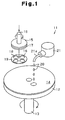
- the polishing apparatus 11 has a disc-type turntable 12 whereon a polishing pad 14 is bonded.
- the turntable 12 rotates around a first rotation shaft 13 installed on the lower center thereof.
- One or a plurality of disc-type wafer holders 15 are installed above the turntable 12, each wafer holder 15 is rotated by a second rotation shaft 16 fixed to the upper center thereof, and a disc-type ceramic plate 17 is fixed to the bottom surface.
- polishing composition 20 is fed to the polishing pad 14 from the nozzle 21a of the feeder 21 installed above the turntable 12.
- a plurality of respectively optimized polishing compositions are prepared for a plurality of polishing processes, and these polishing compositions are separately fed to the polishing pad 14 from a plurality of feeders 21.
- the silicon wafer is first held in the wafer holder 15 by, for example, suction while being accommodated in a wafer-holding hole 18 with the surface to be polished facing downward.
- the polishing composition for first polishing is fed to the polishing pad 14 from the feeder 21.
- the wafer holder 15 is moved downward to push a silicon wafer against the polishing pad 14.
- the first polishing is performed on the wafer surface.
- second polishing is performed.
- the wafer holder 15 is once separated from the turntable 12. While feeding the composition for second polishing onto the polishing pad 14 from the feeder for the second polishing, the wafer holder 15 is moved downward to push a silicon wafer against the polishing pad 14. Thus, the second polishing is performed on the wafer surface.
- third polishing for lowering the haze level of the wafer surface is performed by using the polishing composition 20 according to the present invention.
- the wafer holder 15 is once separated from the turntable 12. While feeding the composition 20 for third polishing onto the polishing pad 14 from the feeder 21 for the third polishing, the wafer holder 15 is moved downward to push a silicon wafer against the polishing pad 14. Thus, the third polishing is performed on the wafer surface.
- the polishing composition of the first embodiment contains HEC and PEO.
- HEC and PEO By the synergic action of HEC and PEO, the surface roughness of wafers is efficiently reduced, and the haze level is reduced in comparison with conventional polishing compositions.
- the adhesion of particles, such as the components of the polishing composition and chips generated by polishing (abrasive shavings) onto the wafer surface is also inhibited, and the deterioration of LPD is prevented.
- the polishing composition contains an alkaline compound (Component C), the polishing speed is improved.
- the second embodiment related to a rinse composition used in the rinsing process performed after the polishing process for reducing the haze level of the wafer surface.
- the rinse composition contains the following components A to D:
- Component C is used in order to adjust the pH of the rinse composition, and to reduce the haze level of the wafer surface. If a rapid change in pH occurs on the surface of a polished wafer, surface roughness is easily produced. Therefore, it is preferred that the pH of the rinse composition is almost the same level as the pH of the polishing composition. If the pH of the rinse composition is considerably lower than the pH of the polishing composition, the polishing composition remaining on the surface of the polishing pad reacts with the rinse composition on the wafer surface to form a gel. Since the removal of the gel from the wafer surface is difficult, and the gel causes the plugging of the polishing pad, the formation of the gel is not preferred. On the other hand, if the pH of the rinse composition is considerably higher than the pH of the polishing composition, the wafer surface is easily roughened.
- the rinse composition is prepared by adding Components A, B, and C to water, and stirring using a blade-type stirrer or dispersing using an ultrasonic dispersing apparatus.
- the order to add Components A, B, and C to water is not limited.
- the polishing composition having a relatively high concentration is prepared in order to facilitate the storage and transportation of the rinse composition.
- the rinse composition is practically used in rinse processes after diluting. For diluting, the above-described impurity-reduced water is used.
- the dilution ratio of the rinse composition is preferably 100 or less, more preferably 80 or less, and most preferably 40 or less. If the dilution ratio exceeds 100, the volume and weight of the diluted solution increase, and the transportation costs tend to be expensive.
- the feeder 21 is replaced with a feeder for the rinse composition while maintaining the state wherein the wafer holder 15 is contacted to the turntable 12.
- the operating conditions of the polishing apparatus are switched to rinse conditions.
- the polishing composition remains on the wafer surface and the polishing pad 14.
- the polishing pad 14 is used as a pad for rinsing.
- the rinse composition is fed onto the polishing pad 14 from the feeder for the rinse composition.
- the wafer surface is rinsed by pushing the silicon wafer against the polishing pad 14.
- the rinse composition of the second embodiment contains HEC and PEO.
- the wafer surface whereon the polishing composition remains is rinsed using the rinse composition. Therefore a mixture of the polishing composition remaining on the wafer surface, the surface on and in the polishing pad, and the rinse composition is formed. Since the mixture contains a trace of silicon dioxide (Component E) derived from the polishing composition, the wafer surface is polished to some extent by silicon dioxide in the rinsing process.
- Component E silicon dioxide
- the polishing and rinsing of the wafer surface are sequentially performed. Therefore, the labor for once removing the silicon wafer after polishing the wafer surface from the wafer holding hole 18, and for mounting the silicon wafer to the rinsing apparatus can be eliminated, and the occurrence of etching or contamination of the wafer surface caused by the polishing composition can be prevented.
- the drying up of the wafer surface after polishing is also prevented, and the adhesion of silicon dioxide in the polishing composition on the wafer surface can be prevented.
- the LPD is improved. Since polishing and rinsing can be performed using the same apparatus, the time for treating the wafer surface can be reduced, and the costs for the polishing and rinsing processes can be reduced.
- the wafer surface may be scrub-cleaned using pure water.
- Scrub cleaning is a method for scrubbing the wafer surface using impurity-reduced water, such as pure water and ultra-pure water, with a sponge made of polyvinyl alcohol or the like.
- the polishing composition and the rinse composition may contain hydrogen peroxide.
- the oxide film formed by hydrogen peroxide on the wafer surface prevents the adhesion of particles directly on the wafer surface, and improves the LPD.
- the rinse composition may contain a trace of silicon dioxide (Component E).
- Component E silicon dioxide
- the polishing composition of Example 1 was prepared by mixing HEC (Component A), PEO (Component B), a 29 wt-% aqueous solution of ammonia (Component C), ultra-pure water (Component D), and colloidal silica (Component E).
- HEC, PEO, and AM in the polishing composition are shown in Table 1.
- the quantity of AM in the following description and tables is the quantity of a 29 wt-% aqueous solution of ammonia
- TMAH is the quantity of a 25 wt-% aqueous solution of TMAH.
- HEC and PEO are components to reduce the haze level
- ammonia is a component to accelerate polishing.
- the content of colloidal silica in the polishing composition was 10% by weight.
- the total content of iron, nickel, copper, and calcium in the 20 wt-% aqueous solution of colloidal silica was 20 ppb or less.
- polishing compositions were prepared in the same manner as in Example 1 except that the kinds and contents of the components to reduce the haze level and the components to accelerate polishing were changed as shown in Tables 1 and 2.
- polishing composition of Examples 1 to 26 and Comparative Examples 1 to 19 was diluted 20 times (volume ratio) with ultra-pure water, and the surface of a silicon wafer was polished using the diluted polishing composition under the following conditions.
- Polishing apparatus Single-side polishing apparatus (SPM-15: Fujikoshi Machinery Corp. with 4 wafer holders) Articles to be polished: Four 6-inch silicon wafers/wafer holder Load: 9.4 kPa Turntable rotating speed: 30 rpm Wafer holder rotating speed: 30 rpm Polishing pad: Surfin 000 (suede type, manufactured by Fujimi Incorporated) Feed speed of the composition: 500 ml/min Polishing time: 8 min Temperature of the composition: 20°C
- the silicon wafers after polishing were subjected to scrub cleaning for 10 seconds using pure water, and SC-1 cleaning.
- HL haze level
- LPD haze level
- Examples 2, 3, 5, and 10 to 14, and Comparative Examples 5, 10 to 13, and 16 the surface conditions were also evaluated. The results of evaluation are shown in Tables 1 and 2.
- the haze levels of silicon wafers after cleaning were measured using an AMS-AWIS 3110 (trade name of ADE Company). The measured haze levels were evaluated by five scales of less than 0.05 ppm ( ). 0.05 ppm or more and less than 0.075 ppm (o ⁇ ), 0.075 ppm or more and less than 0.1 ppm ( ⁇ ), 0.1 ppm or more and less than 0.2 ppm ( ⁇ ), and 0.2 ppm or more ( ⁇ ).
- the number of particles of a size of 0.1 ⁇ m or larger in silicon wafers after cleaning was counted using an AMS-AWIS 3110.
- the LPD was evaluated by three scales of less than 50 ( ⁇ ), 50 or more and less than 300 ( ⁇ ), and 300 or more ( ⁇ ).
- the surface conditions of silicon wafers after cleaning were observed using an atomic force microscope (D 3000 manufactured by Digital Instruments). The observed range was a square area of a side of 10 ⁇ m, and ten areas were observed. The surface conditions were evaluated by four scales of very good without scratches (o ⁇ ), good with few scratches ( ⁇ ), poor with scratches ( ⁇ ), and very poor with many scratches ( ⁇ ).
- polishing compositions of Examples 1 to 26 that contained both HEC and PEO were superior to the polishing compositions of Comparative Examples 1 to 19 that lacked at least one of HEC and PEO.
- Rinse compositions of Example 27 was prepared by mixing HEC (Component A), PEO (Component B), AM (Component C), and ultra-pure water (Component D).
- HEC and PEO are the component to reduce the haze level
- Component C is a component to adjust pH.
- the contents of HEC, PEO, and AM in the rinse composition are shown in Table 3.
- compositions of the rinse compositions of Examples 28 to 52 and Comparative Examples 20 to 36 are shown in Tables 3 and 4. Each rinse composition of Examples 27 to 52 and Comparative Examples 20 to 36 was diluted 20 times with ultra-pure water.
- the operating conditions of the polishing apparatus were switched to the following rinsing conditions, and rinsing was performed using the diluted rinse composition.
- the rinsing tests for the rinse compositions of Example 51 and Comparative Example 35 were different from the tests for the rinse compositions of Examples 27 to 50 and Comparative Examples 20 to 34 only in the following aspects.
- the silicon wafers for the tests were 6-inch silicon wafers (p-type, crystal orientation ⁇ 100>, resistivity: 0.01 ⁇ cm or more and less than 0.1 ⁇ cm) from which the surface layers had been previously removed by 10 ⁇ m by polishing using a polishing composition (GLANZOX-1101, manufactured by Fujimi Incorporated), and polished using the polishing composition of Comparative Example 19 before rinsing.
- the rinsing tests for the rinse compositions of Example 52 and Comparative Example 36 were different from the tests for the rinse compositions of Examples 27 to 50 and Comparative Examples 20 to 34 only in the following aspects.
- the silicon wafers for the tests were 6-inch silicon wafers (p-type, crystal orientation ⁇ 100>, resistivity: 0.1 ⁇ cm or more) from which the surface layers had been previously removed by 10 ⁇ m by polishing using a polishing composition (GLANZOX-1101, manufactured by Fujimi Incorporated).
- the evaluations of the haze level were low in the rinse compositions of Comparative Examples 20, 21, 25 to 28, and 32 to 34 that contained either one of HEC or PEO; the rinse compositions of Comparative Examples 22 to 24 and 31 that contained neither HEC nor PEO; the rinse composition of Comparative Example 29 that contained 0.005% by weight or less PEO; the rinse composition of Comparative Example 30 that contained 0.5% by weight or more PEO; and Comparative Examples 35 and 36 that contained either one of HEC or PEO.
Landscapes
- Chemical & Material Sciences (AREA)
- Organic Chemistry (AREA)
- Engineering & Computer Science (AREA)
- Life Sciences & Earth Sciences (AREA)
- Oil, Petroleum & Natural Gas (AREA)
- Chemical Kinetics & Catalysis (AREA)
- Health & Medical Sciences (AREA)
- Wood Science & Technology (AREA)
- Emergency Medicine (AREA)
- Materials Engineering (AREA)
- Molecular Biology (AREA)
- Inorganic Chemistry (AREA)
- Mechanical Treatment Of Semiconductor (AREA)
- Finish Polishing, Edge Sharpening, And Grinding By Specific Grinding Devices (AREA)
- Cleaning Or Drying Semiconductors (AREA)
Applications Claiming Priority (2)
| Application Number | Priority Date | Filing Date | Title |
|---|---|---|---|
| JP2002287979A JP4212861B2 (ja) | 2002-09-30 | 2002-09-30 | 研磨用組成物及びそれを用いたシリコンウエハの研磨方法、並びにリンス用組成物及びそれを用いたシリコンウエハのリンス方法 |
| JP2002287979 | 2002-09-30 |
Publications (2)
| Publication Number | Publication Date |
|---|---|
| EP1424727A1 true EP1424727A1 (de) | 2004-06-02 |
| EP1424727B1 EP1424727B1 (de) | 2007-12-19 |
Family
ID=32280597
Family Applications (1)
| Application Number | Title | Priority Date | Filing Date |
|---|---|---|---|
| EP03022114A Expired - Lifetime EP1424727B1 (de) | 2002-09-30 | 2003-09-29 | Polierzusammensetzung und Waschzusammensetzung |
Country Status (5)
| Country | Link |
|---|---|
| US (3) | US7211122B2 (de) |
| EP (1) | EP1424727B1 (de) |
| JP (1) | JP4212861B2 (de) |
| KR (1) | KR101010586B1 (de) |
| DE (1) | DE60318172T2 (de) |
Cited By (7)
| Publication number | Priority date | Publication date | Assignee | Title |
|---|---|---|---|---|
| EP1405885A3 (de) * | 2002-09-30 | 2004-11-24 | Fujimi Incorporated | Zusammensetzung zum Polieren von Halbleiterscheiben und Verfahren zur Verwendung derselben |
| GB2416354A (en) * | 2004-06-18 | 2006-01-25 | Fujimi Inc | Rinsing composition and use thereof in rinsing silicon wafers |
| WO2007041203A1 (en) * | 2005-10-04 | 2007-04-12 | Cabot Microelectronics Corporation | Method for controlling polysilicon removal |
| GB2434799A (en) * | 2006-02-07 | 2007-08-08 | Fujimi Inc | Polishing composition and polishing method |
| EP3258483A4 (de) * | 2015-02-12 | 2018-02-28 | Fujimi Incorporated | Verfahren zum polieren eines siliciumwafers und oberflächenbehandlungszusammensetzung |
| CN109648450A (zh) * | 2018-12-28 | 2019-04-19 | 临安宇杰精密制品有限公司 | 一种精密元件的抛光、清洗工艺 |
| US10748778B2 (en) | 2015-02-12 | 2020-08-18 | Fujimi Incorporated | Method for polishing silicon wafer and surface treatment composition |
Families Citing this family (55)
| Publication number | Priority date | Publication date | Assignee | Title |
|---|---|---|---|---|
| EP1564797B1 (de) * | 2002-11-08 | 2016-07-27 | Fujimi Incorporated | Polierzusammensetzung und spülzusammensetzung |
| JP4668528B2 (ja) * | 2003-09-05 | 2011-04-13 | 株式会社フジミインコーポレーテッド | 研磨用組成物 |
| WO2005029563A1 (ja) * | 2003-09-24 | 2005-03-31 | Nippon Chemical Industrial Co.,Ltd. | シリコンウエハ研磨用組成物および研磨方法 |
| JP2005268665A (ja) * | 2004-03-19 | 2005-09-29 | Fujimi Inc | 研磨用組成物 |
| JP2005268667A (ja) * | 2004-03-19 | 2005-09-29 | Fujimi Inc | 研磨用組成物 |
| JP4284215B2 (ja) * | 2004-03-24 | 2009-06-24 | 株式会社東芝 | 基板処理方法 |
| JP5164129B2 (ja) * | 2004-03-29 | 2013-03-13 | ニッタ・ハース株式会社 | 半導体研磨用組成物 |
| JP2005303060A (ja) * | 2004-04-13 | 2005-10-27 | Nitta Haas Inc | リンス研磨溶液 |
| JP4814502B2 (ja) * | 2004-09-09 | 2011-11-16 | 株式会社フジミインコーポレーテッド | 研磨用組成物及びそれを用いた研磨方法 |
| JP4808394B2 (ja) * | 2004-10-29 | 2011-11-02 | 株式会社フジミインコーポレーテッド | 研磨用組成物 |
| US7351662B2 (en) * | 2005-01-07 | 2008-04-01 | Dupont Air Products Nanomaterials Llc | Composition and associated method for catalyzing removal rates of dielectric films during chemical mechanical planarization |
| JP2007063374A (ja) * | 2005-08-30 | 2007-03-15 | Nitta Haas Inc | 研磨組成物用添加剤 |
| JP4476232B2 (ja) * | 2006-03-10 | 2010-06-09 | 三菱重工業株式会社 | 成膜装置のシーズニング方法 |
| JP5335183B2 (ja) * | 2006-08-24 | 2013-11-06 | 株式会社フジミインコーポレーテッド | 研磨用組成物及び研磨方法 |
| JP5204960B2 (ja) * | 2006-08-24 | 2013-06-05 | 株式会社フジミインコーポレーテッド | 研磨用組成物及び研磨方法 |
| JP5357396B2 (ja) * | 2007-01-31 | 2013-12-04 | ニッタ・ハース株式会社 | 研磨組成物用添加剤および研磨組成物の使用方法 |
| US8226775B2 (en) * | 2007-12-14 | 2012-07-24 | Lam Research Corporation | Methods for particle removal by single-phase and two-phase media |
| JP5575735B2 (ja) * | 2008-07-03 | 2014-08-20 | 株式会社フジミインコーポレーテッド | 研磨用組成物濃縮物 |
| JP5474400B2 (ja) * | 2008-07-03 | 2014-04-16 | 株式会社フジミインコーポレーテッド | 半導体用濡れ剤、それを用いた研磨用組成物および研磨方法 |
| DE102008044646B4 (de) * | 2008-08-27 | 2011-06-22 | Siltronic AG, 81737 | Verfahren zur Herstellung einer Halbleiterscheibe |
| KR101439995B1 (ko) * | 2010-04-30 | 2014-09-12 | 가부시키가이샤 사무코 | 실리콘 웨이퍼의 연마 방법 |
| WO2012002525A1 (ja) * | 2010-07-02 | 2012-01-05 | 株式会社Sumco | シリコンウェーハの研磨方法 |
| JP5585652B2 (ja) * | 2010-07-08 | 2014-09-10 | 株式会社Sumco | シリコンウェーハの研磨方法 |
| US9028709B2 (en) | 2010-09-27 | 2015-05-12 | Fujimi Incorporated | Surface treatment composition and surface treatment method using same |
| WO2012102144A1 (ja) * | 2011-01-26 | 2012-08-02 | 株式会社 フジミインコーポレーテッド | 研磨用組成物、それを用いた研磨方法及び基板の製造方法 |
| US8309468B1 (en) * | 2011-04-28 | 2012-11-13 | Rohm And Haas Electronic Materials Cmp Holdings, Inc. | Chemical mechanical polishing composition and method for polishing germanium-antimony-tellurium alloys |
| US8790160B2 (en) * | 2011-04-28 | 2014-07-29 | Rohm And Haas Electronic Materials Cmp Holdings, Inc. | Chemical mechanical polishing composition and method for polishing phase change alloys |
| US8513128B2 (en) | 2011-06-17 | 2013-08-20 | United Microelectronics Corp. | Poly opening polish process |
| US8643069B2 (en) | 2011-07-12 | 2014-02-04 | United Microelectronics Corp. | Semiconductor device having metal gate and manufacturing method thereof |
| DE112012004431B4 (de) | 2011-10-24 | 2025-12-31 | Fujimi Incorporated | Zusammensetzung zu Polierzwecken, Polierverfahren unter Verwendung derselben und Verfahren zur Herstellung eines Substrates |
| US8673755B2 (en) | 2011-10-27 | 2014-03-18 | United Microelectronics Corp. | Semiconductor device having metal gate and manufacturing method thereof |
| US9006010B2 (en) * | 2011-11-22 | 2015-04-14 | General Electric Company | Radiation detectors and methods of fabricating radiation detectors |
| JP5822356B2 (ja) | 2012-04-17 | 2015-11-24 | 花王株式会社 | シリコンウェーハ用研磨液組成物 |
| US9136170B2 (en) | 2012-05-30 | 2015-09-15 | United Microelectronics Corp. | Through silicon via (TSV) structure and process thereof |
| JP2014080461A (ja) * | 2012-10-12 | 2014-05-08 | Fujimi Inc | 研磨用組成物の製造方法及び研磨用組成物 |
| US20150376464A1 (en) * | 2013-02-13 | 2015-12-31 | Fujimi Incorporated | Polishing composition, method for producing polishing composition and method for producing polished article |
| CN105073941B (zh) | 2013-02-21 | 2018-01-30 | 福吉米株式会社 | 研磨用组合物及研磨物制造方法 |
| US8836129B1 (en) | 2013-03-14 | 2014-09-16 | United Microelectronics Corp. | Plug structure |
| JP2014216464A (ja) | 2013-04-25 | 2014-11-17 | 日本キャボット・マイクロエレクトロニクス株式会社 | スラリー組成物および基板研磨方法 |
| CN105451940B (zh) * | 2013-08-09 | 2018-12-11 | 福吉米株式会社 | 研磨完的研磨对象物的制造方法及研磨用组合物试剂盒 |
| JP5893706B2 (ja) | 2013-10-25 | 2016-03-23 | 花王株式会社 | シリコンウェーハ用研磨液組成物 |
| JP6266337B2 (ja) | 2013-12-25 | 2018-01-24 | ニッタ・ハース株式会社 | 半導体基板用濡れ剤及び研磨用組成物 |
| JP6343160B2 (ja) * | 2014-03-28 | 2018-06-13 | 株式会社フジミインコーポレーテッド | 研磨用組成物 |
| JP6389630B2 (ja) | 2014-03-31 | 2018-09-12 | ニッタ・ハース株式会社 | 研磨用組成物 |
| JP6389629B2 (ja) | 2014-03-31 | 2018-09-12 | ニッタ・ハース株式会社 | 研磨用組成物 |
| JP6314019B2 (ja) | 2014-03-31 | 2018-04-18 | ニッタ・ハース株式会社 | 半導体基板の研磨方法 |
| CN108138032B (zh) * | 2015-10-23 | 2021-02-12 | 霓达杜邦股份有限公司 | 研磨用组合物 |
| JP6796978B2 (ja) * | 2016-09-23 | 2020-12-09 | 株式会社岡本工作機械製作所 | 半導体装置の製造方法 |
| WO2018079675A1 (ja) | 2016-10-28 | 2018-05-03 | 花王株式会社 | シリコンウェーハ用リンス剤組成物 |
| JP7061862B2 (ja) | 2016-10-28 | 2022-05-02 | 花王株式会社 | シリコンウェーハ用リンス剤組成物 |
| JP6495230B2 (ja) | 2016-12-22 | 2019-04-03 | 花王株式会社 | シリコンウェーハ用リンス剤組成物 |
| KR102685348B1 (ko) | 2017-11-06 | 2024-07-17 | 가부시키가이샤 후지미인코퍼레이티드 | 연마용 조성물 및 그의 제조 방법 |
| US20210277282A1 (en) * | 2018-07-04 | 2021-09-09 | Sumitomo Seika Chemicals Co., Ltd. | Polishing composition |
| KR102904899B1 (ko) | 2019-02-21 | 2025-12-30 | 미쯔비시 케미컬 주식회사 | 실리카 입자와 그 제조 방법, 실리카졸, 연마 조성물, 연마 방법, 반도체 웨이퍼의 제조 방법 및 반도체 디바이스의 제조 방법 |
| JP2019131814A (ja) * | 2019-03-08 | 2019-08-08 | 株式会社フジミインコーポレーテッド | 研磨用組成物の製造方法 |
Citations (3)
| Publication number | Priority date | Publication date | Assignee | Title |
|---|---|---|---|---|
| JPS63272459A (ja) * | 1987-04-27 | 1988-11-09 | Mitsubishi Monsanto Chem Co | ウエハ−のフアイン研磨用の組成物 |
| EP0373501A2 (de) * | 1988-12-12 | 1990-06-20 | E.I. Du Pont De Nemours And Company | Feine Polierzusammensetzung für Plaketten |
| US6258721B1 (en) * | 1999-12-27 | 2001-07-10 | General Electric Company | Diamond slurry for chemical-mechanical planarization of semiconductor wafers |
Family Cites Families (15)
| Publication number | Priority date | Publication date | Assignee | Title |
|---|---|---|---|---|
| US3715842A (en) * | 1970-07-02 | 1973-02-13 | Tizon Chem Corp | Silica polishing compositions having a reduced tendency to scratch silicon and germanium surfaces |
| US4169337A (en) * | 1978-03-30 | 1979-10-02 | Nalco Chemical Company | Process for polishing semi-conductor materials |
| US4462188A (en) * | 1982-06-21 | 1984-07-31 | Nalco Chemical Company | Silica sol compositions for polishing silicon wafers |
| US4588421A (en) * | 1984-10-15 | 1986-05-13 | Nalco Chemical Company | Aqueous silica compositions for polishing silicon wafers |
| US5352277A (en) * | 1988-12-12 | 1994-10-04 | E. I. Du Pont De Nemours & Company | Final polishing composition |
| US5053448A (en) * | 1989-07-21 | 1991-10-01 | S. C. Johnson & Son, Inc. | Polymeric thickener and methods of producing the same |
| JP4115562B2 (ja) | 1997-10-14 | 2008-07-09 | 株式会社フジミインコーポレーテッド | 研磨用組成物 |
| US6110830A (en) * | 1998-04-24 | 2000-08-29 | Micron Technology, Inc. | Methods of reducing corrosion of materials, methods of protecting aluminum within aluminum-comprising layers from electrochemical degradation during semiconductor processing methods of forming aluminum-comprising lines |
| JPH11349925A (ja) * | 1998-06-05 | 1999-12-21 | Fujimi Inc | エッジポリッシング用組成物 |
| JP3810588B2 (ja) * | 1998-06-22 | 2006-08-16 | 株式会社フジミインコーポレーテッド | 研磨用組成物 |
| US6258140B1 (en) * | 1999-09-27 | 2001-07-10 | Fujimi America Inc. | Polishing composition |
| US6709981B2 (en) * | 2000-08-16 | 2004-03-23 | Memc Electronic Materials, Inc. | Method and apparatus for processing a semiconductor wafer using novel final polishing method |
| CN1193410C (zh) * | 2000-09-01 | 2005-03-16 | 株式会社德山 | 残渣洗涤液 |
| JP3768401B2 (ja) * | 2000-11-24 | 2006-04-19 | Necエレクトロニクス株式会社 | 化学的機械的研磨用スラリー |
| JP3440419B2 (ja) * | 2001-02-02 | 2003-08-25 | 株式会社フジミインコーポレーテッド | 研磨用組成物およびそれを用いた研磨方法 |
-
2002
- 2002-09-30 JP JP2002287979A patent/JP4212861B2/ja not_active Expired - Fee Related
-
2003
- 2003-09-29 EP EP03022114A patent/EP1424727B1/de not_active Expired - Lifetime
- 2003-09-29 US US10/674,209 patent/US7211122B2/en not_active Expired - Fee Related
- 2003-09-29 DE DE60318172T patent/DE60318172T2/de not_active Expired - Lifetime
- 2003-09-30 KR KR1020030067778A patent/KR101010586B1/ko not_active Expired - Fee Related
-
2007
- 2007-04-25 US US11/740,005 patent/US20070186485A1/en not_active Abandoned
- 2007-04-25 US US11/740,034 patent/US7687393B2/en not_active Expired - Fee Related
Patent Citations (3)
| Publication number | Priority date | Publication date | Assignee | Title |
|---|---|---|---|---|
| JPS63272459A (ja) * | 1987-04-27 | 1988-11-09 | Mitsubishi Monsanto Chem Co | ウエハ−のフアイン研磨用の組成物 |
| EP0373501A2 (de) * | 1988-12-12 | 1990-06-20 | E.I. Du Pont De Nemours And Company | Feine Polierzusammensetzung für Plaketten |
| US6258721B1 (en) * | 1999-12-27 | 2001-07-10 | General Electric Company | Diamond slurry for chemical-mechanical planarization of semiconductor wafers |
Non-Patent Citations (1)
| Title |
|---|
| PATENT ABSTRACTS OF JAPAN vol. 0130, no. 71 (M - 799) 17 February 1989 (1989-02-17) * |
Cited By (10)
| Publication number | Priority date | Publication date | Assignee | Title |
|---|---|---|---|---|
| EP1405885A3 (de) * | 2002-09-30 | 2004-11-24 | Fujimi Incorporated | Zusammensetzung zum Polieren von Halbleiterscheiben und Verfahren zur Verwendung derselben |
| US7052522B2 (en) | 2002-09-30 | 2006-05-30 | Fujimi Incorporated | Polishing composition and polishing method using the same |
| GB2416354A (en) * | 2004-06-18 | 2006-01-25 | Fujimi Inc | Rinsing composition and use thereof in rinsing silicon wafers |
| GB2416354B (en) * | 2004-06-18 | 2009-05-27 | Fujimi Inc | Rinsing composition and method for rinsing and manufacturing silicon wafer |
| WO2007041203A1 (en) * | 2005-10-04 | 2007-04-12 | Cabot Microelectronics Corporation | Method for controlling polysilicon removal |
| GB2434799A (en) * | 2006-02-07 | 2007-08-08 | Fujimi Inc | Polishing composition and polishing method |
| US7998229B2 (en) | 2006-02-07 | 2011-08-16 | Fujimi Incorporated | Polishing composition and polishing method |
| EP3258483A4 (de) * | 2015-02-12 | 2018-02-28 | Fujimi Incorporated | Verfahren zum polieren eines siliciumwafers und oberflächenbehandlungszusammensetzung |
| US10748778B2 (en) | 2015-02-12 | 2020-08-18 | Fujimi Incorporated | Method for polishing silicon wafer and surface treatment composition |
| CN109648450A (zh) * | 2018-12-28 | 2019-04-19 | 临安宇杰精密制品有限公司 | 一种精密元件的抛光、清洗工艺 |
Also Published As
| Publication number | Publication date |
|---|---|
| KR20040032051A (ko) | 2004-04-14 |
| US20070186485A1 (en) | 2007-08-16 |
| US20070186486A1 (en) | 2007-08-16 |
| JP4212861B2 (ja) | 2009-01-21 |
| DE60318172D1 (de) | 2008-01-31 |
| US7211122B2 (en) | 2007-05-01 |
| EP1424727B1 (de) | 2007-12-19 |
| JP2004128089A (ja) | 2004-04-22 |
| DE60318172T2 (de) | 2008-12-18 |
| US20040098924A1 (en) | 2004-05-27 |
| US7687393B2 (en) | 2010-03-30 |
| KR101010586B1 (ko) | 2011-01-24 |
Similar Documents
| Publication | Publication Date | Title |
|---|---|---|
| US7211122B2 (en) | Polishing composition and rinse composition | |
| EP1512732B1 (de) | Polierzusammensetzung | |
| EP1564797B1 (de) | Polierzusammensetzung und spülzusammensetzung | |
| JP6068647B2 (ja) | 研磨済研磨対象物の製造方法および研磨用組成物キット | |
| CN105264647B (zh) | 硅晶圆研磨用组合物 | |
| US10344185B2 (en) | Composition for polishing silicon wafers | |
| JP7862133B2 (ja) | 化学機械研磨組成物、リンス組成物、基材の化学機械研磨方法及び基材のリンス方法 | |
| JP2008053415A (ja) | 研磨用組成物及び研磨方法 | |
| JP6350861B2 (ja) | コロイダルシリカ及びそれを含有する半導体ウエハ研磨用組成物 | |
| JP6348927B2 (ja) | シリコンウェーハ研磨用組成物 | |
| CN101050348A (zh) | 蚀刻液组合物、研磨用组合物及其制造方法以及研磨方法 | |
| WO2017150157A1 (ja) | シリコン基板の研磨方法および研磨用組成物セット | |
| TW202033689A (zh) | 研磨用組合物 | |
| US11939491B2 (en) | Method of polishing object to be polished containing material having silicon-silicon bond | |
| TW202446901A (zh) | 研磨用組成物、研磨用組成物之濃縮液及研磨方法 | |
| TW202134363A (zh) | 研磨用組合物及矽晶圓之研磨方法 |
Legal Events
| Date | Code | Title | Description |
|---|---|---|---|
| PUAI | Public reference made under article 153(3) epc to a published international application that has entered the european phase |
Free format text: ORIGINAL CODE: 0009012 |
|
| AK | Designated contracting states |
Kind code of ref document: A1 Designated state(s): AT BE BG CH CY CZ DE DK EE ES FI FR GB GR HU IE IT LI LU MC NL PT RO SE SI SK TR |
|
| AX | Request for extension of the european patent |
Extension state: AL LT LV MK |
|
| 17P | Request for examination filed |
Effective date: 20041118 |
|
| AKX | Designation fees paid |
Designated state(s): DE GB |
|
| RBV | Designated contracting states (corrected) |
Designated state(s): DE GB |
|
| GRAP | Despatch of communication of intention to grant a patent |
Free format text: ORIGINAL CODE: EPIDOSNIGR1 |
|
| GRAS | Grant fee paid |
Free format text: ORIGINAL CODE: EPIDOSNIGR3 |
|
| GRAA | (expected) grant |
Free format text: ORIGINAL CODE: 0009210 |
|
| AK | Designated contracting states |
Kind code of ref document: B1 Designated state(s): DE GB |
|
| REG | Reference to a national code |
Ref country code: GB Ref legal event code: FG4D |
|
| REF | Corresponds to: |
Ref document number: 60318172 Country of ref document: DE Date of ref document: 20080131 Kind code of ref document: P |
|
| PLBE | No opposition filed within time limit |
Free format text: ORIGINAL CODE: 0009261 |
|
| STAA | Information on the status of an ep patent application or granted ep patent |
Free format text: STATUS: NO OPPOSITION FILED WITHIN TIME LIMIT |
|
| 26N | No opposition filed |
Effective date: 20080922 |
|
| PGFP | Annual fee paid to national office [announced via postgrant information from national office to epo] |
Ref country code: DE Payment date: 20130927 Year of fee payment: 11 |
|
| PGFP | Annual fee paid to national office [announced via postgrant information from national office to epo] |
Ref country code: GB Payment date: 20130925 Year of fee payment: 11 |
|
| REG | Reference to a national code |
Ref country code: DE Ref legal event code: R119 Ref document number: 60318172 Country of ref document: DE |
|
| GBPC | Gb: european patent ceased through non-payment of renewal fee |
Effective date: 20140929 |
|
| PG25 | Lapsed in a contracting state [announced via postgrant information from national office to epo] |
Ref country code: GB Free format text: LAPSE BECAUSE OF NON-PAYMENT OF DUE FEES Effective date: 20140929 Ref country code: DE Free format text: LAPSE BECAUSE OF NON-PAYMENT OF DUE FEES Effective date: 20150401 |