EP1426189A2 - Thermisches Übertragungselement für den Transfer durch Laser mit eigener Dotierschicht - Google Patents
Thermisches Übertragungselement für den Transfer durch Laser mit eigener Dotierschicht Download PDFInfo
- Publication number
- EP1426189A2 EP1426189A2 EP03077293A EP03077293A EP1426189A2 EP 1426189 A2 EP1426189 A2 EP 1426189A2 EP 03077293 A EP03077293 A EP 03077293A EP 03077293 A EP03077293 A EP 03077293A EP 1426189 A2 EP1426189 A2 EP 1426189A2
- Authority
- EP
- European Patent Office
- Prior art keywords
- light
- layer
- donor
- dopant
- donor element
- Prior art date
- Legal status (The legal status is an assumption and is not a legal conclusion. Google has not performed a legal analysis and makes no representation as to the accuracy of the status listed.)
- Withdrawn
Links
Images



Classifications
-
- C—CHEMISTRY; METALLURGY
- C23—COATING METALLIC MATERIAL; COATING MATERIAL WITH METALLIC MATERIAL; CHEMICAL SURFACE TREATMENT; DIFFUSION TREATMENT OF METALLIC MATERIAL; COATING BY VACUUM EVAPORATION, BY SPUTTERING, BY ION IMPLANTATION OR BY CHEMICAL VAPOUR DEPOSITION, IN GENERAL; INHIBITING CORROSION OF METALLIC MATERIAL OR INCRUSTATION IN GENERAL
- C23C—COATING METALLIC MATERIAL; COATING MATERIAL WITH METALLIC MATERIAL; SURFACE TREATMENT OF METALLIC MATERIAL BY DIFFUSION INTO THE SURFACE, BY CHEMICAL CONVERSION OR SUBSTITUTION; COATING BY VACUUM EVAPORATION, BY SPUTTERING, BY ION IMPLANTATION OR BY CHEMICAL VAPOUR DEPOSITION, IN GENERAL
- C23C14/00—Coating by vacuum evaporation, by sputtering or by ion implantation of the coating forming material
- C23C14/22—Coating by vacuum evaporation, by sputtering or by ion implantation of the coating forming material characterised by the process of coating
- C23C14/24—Vacuum evaporation
- C23C14/28—Vacuum evaporation by wave energy or particle radiation
-
- B—PERFORMING OPERATIONS; TRANSPORTING
- B41—PRINTING; LINING MACHINES; TYPEWRITERS; STAMPS
- B41M—PRINTING, DUPLICATING, MARKING, OR COPYING PROCESSES; COLOUR PRINTING
- B41M5/00—Duplicating or marking methods; Sheet materials for use therein
- B41M5/26—Thermography ; Marking by high energetic means, e.g. laser otherwise than by burning, and characterised by the material used
- B41M5/265—Thermography ; Marking by high energetic means, e.g. laser otherwise than by burning, and characterised by the material used for the production of optical filters or electrical components
-
- C—CHEMISTRY; METALLURGY
- C09—DYES; PAINTS; POLISHES; NATURAL RESINS; ADHESIVES; COMPOSITIONS NOT OTHERWISE PROVIDED FOR; APPLICATIONS OF MATERIALS NOT OTHERWISE PROVIDED FOR
- C09K—MATERIALS FOR MISCELLANEOUS APPLICATIONS, NOT PROVIDED FOR ELSEWHERE
- C09K11/00—Luminescent materials, e.g. electroluminescent or chemiluminescent
- C09K11/06—Luminescent materials, e.g. electroluminescent or chemiluminescent containing organic luminescent materials
-
- C—CHEMISTRY; METALLURGY
- C23—COATING METALLIC MATERIAL; COATING MATERIAL WITH METALLIC MATERIAL; CHEMICAL SURFACE TREATMENT; DIFFUSION TREATMENT OF METALLIC MATERIAL; COATING BY VACUUM EVAPORATION, BY SPUTTERING, BY ION IMPLANTATION OR BY CHEMICAL VAPOUR DEPOSITION, IN GENERAL; INHIBITING CORROSION OF METALLIC MATERIAL OR INCRUSTATION IN GENERAL
- C23C—COATING METALLIC MATERIAL; COATING MATERIAL WITH METALLIC MATERIAL; SURFACE TREATMENT OF METALLIC MATERIAL BY DIFFUSION INTO THE SURFACE, BY CHEMICAL CONVERSION OR SUBSTITUTION; COATING BY VACUUM EVAPORATION, BY SPUTTERING, BY ION IMPLANTATION OR BY CHEMICAL VAPOUR DEPOSITION, IN GENERAL
- C23C14/00—Coating by vacuum evaporation, by sputtering or by ion implantation of the coating forming material
- C23C14/04—Coating on selected surface areas, e.g. using masks
- C23C14/048—Coating on selected surface areas, e.g. using masks using irradiation by energy or particles
-
- C—CHEMISTRY; METALLURGY
- C23—COATING METALLIC MATERIAL; COATING MATERIAL WITH METALLIC MATERIAL; CHEMICAL SURFACE TREATMENT; DIFFUSION TREATMENT OF METALLIC MATERIAL; COATING BY VACUUM EVAPORATION, BY SPUTTERING, BY ION IMPLANTATION OR BY CHEMICAL VAPOUR DEPOSITION, IN GENERAL; INHIBITING CORROSION OF METALLIC MATERIAL OR INCRUSTATION IN GENERAL
- C23C—COATING METALLIC MATERIAL; COATING MATERIAL WITH METALLIC MATERIAL; SURFACE TREATMENT OF METALLIC MATERIAL BY DIFFUSION INTO THE SURFACE, BY CHEMICAL CONVERSION OR SUBSTITUTION; COATING BY VACUUM EVAPORATION, BY SPUTTERING, BY ION IMPLANTATION OR BY CHEMICAL VAPOUR DEPOSITION, IN GENERAL
- C23C14/00—Coating by vacuum evaporation, by sputtering or by ion implantation of the coating forming material
- C23C14/06—Coating by vacuum evaporation, by sputtering or by ion implantation of the coating forming material characterised by the coating material
- C23C14/12—Organic material
-
- H—ELECTRICITY
- H05—ELECTRIC TECHNIQUES NOT OTHERWISE PROVIDED FOR
- H05B—ELECTRIC HEATING; ELECTRIC LIGHT SOURCES NOT OTHERWISE PROVIDED FOR; CIRCUIT ARRANGEMENTS FOR ELECTRIC LIGHT SOURCES, IN GENERAL
- H05B33/00—Electroluminescent light sources
- H05B33/10—Apparatus or processes specially adapted to the manufacture of electroluminescent light sources
-
- H—ELECTRICITY
- H05—ELECTRIC TECHNIQUES NOT OTHERWISE PROVIDED FOR
- H05B—ELECTRIC HEATING; ELECTRIC LIGHT SOURCES NOT OTHERWISE PROVIDED FOR; CIRCUIT ARRANGEMENTS FOR ELECTRIC LIGHT SOURCES, IN GENERAL
- H05B33/00—Electroluminescent light sources
- H05B33/12—Light sources with substantially two-dimensional [2D] radiating surfaces
- H05B33/22—Light sources with substantially two-dimensional [2D] radiating surfaces characterised by the chemical or physical composition or the arrangement of auxiliary dielectric or reflective layers
-
- H—ELECTRICITY
- H10—SEMICONDUCTOR DEVICES; ELECTRIC SOLID-STATE DEVICES NOT OTHERWISE PROVIDED FOR
- H10K—ORGANIC ELECTRIC SOLID-STATE DEVICES
- H10K71/00—Manufacture or treatment specially adapted for the organic devices covered by this subclass
- H10K71/10—Deposition of organic active material
- H10K71/18—Deposition of organic active material using non-liquid printing techniques, e.g. thermal transfer printing from a donor sheet
-
- B—PERFORMING OPERATIONS; TRANSPORTING
- B41—PRINTING; LINING MACHINES; TYPEWRITERS; STAMPS
- B41M—PRINTING, DUPLICATING, MARKING, OR COPYING PROCESSES; COLOUR PRINTING
- B41M2205/00—Printing methods or features related to printing methods; Location or type of the layers
- B41M2205/02—Dye diffusion thermal transfer printing (D2T2)
-
- C—CHEMISTRY; METALLURGY
- C09—DYES; PAINTS; POLISHES; NATURAL RESINS; ADHESIVES; COMPOSITIONS NOT OTHERWISE PROVIDED FOR; APPLICATIONS OF MATERIALS NOT OTHERWISE PROVIDED FOR
- C09K—MATERIALS FOR MISCELLANEOUS APPLICATIONS, NOT PROVIDED FOR ELSEWHERE
- C09K2211/00—Chemical nature of organic luminescent or tenebrescent compounds
- C09K2211/10—Non-macromolecular compounds
- C09K2211/1003—Carbocyclic compounds
- C09K2211/1011—Condensed systems
-
- C—CHEMISTRY; METALLURGY
- C09—DYES; PAINTS; POLISHES; NATURAL RESINS; ADHESIVES; COMPOSITIONS NOT OTHERWISE PROVIDED FOR; APPLICATIONS OF MATERIALS NOT OTHERWISE PROVIDED FOR
- C09K—MATERIALS FOR MISCELLANEOUS APPLICATIONS, NOT PROVIDED FOR ELSEWHERE
- C09K2211/00—Chemical nature of organic luminescent or tenebrescent compounds
- C09K2211/10—Non-macromolecular compounds
- C09K2211/1018—Heterocyclic compounds
- C09K2211/1025—Heterocyclic compounds characterised by ligands
- C09K2211/1029—Heterocyclic compounds characterised by ligands containing one nitrogen atom as the heteroatom
-
- C—CHEMISTRY; METALLURGY
- C09—DYES; PAINTS; POLISHES; NATURAL RESINS; ADHESIVES; COMPOSITIONS NOT OTHERWISE PROVIDED FOR; APPLICATIONS OF MATERIALS NOT OTHERWISE PROVIDED FOR
- C09K—MATERIALS FOR MISCELLANEOUS APPLICATIONS, NOT PROVIDED FOR ELSEWHERE
- C09K2211/00—Chemical nature of organic luminescent or tenebrescent compounds
- C09K2211/10—Non-macromolecular compounds
- C09K2211/1018—Heterocyclic compounds
- C09K2211/1025—Heterocyclic compounds characterised by ligands
- C09K2211/1029—Heterocyclic compounds characterised by ligands containing one nitrogen atom as the heteroatom
- C09K2211/1033—Heterocyclic compounds characterised by ligands containing one nitrogen atom as the heteroatom with oxygen
-
- C—CHEMISTRY; METALLURGY
- C09—DYES; PAINTS; POLISHES; NATURAL RESINS; ADHESIVES; COMPOSITIONS NOT OTHERWISE PROVIDED FOR; APPLICATIONS OF MATERIALS NOT OTHERWISE PROVIDED FOR
- C09K—MATERIALS FOR MISCELLANEOUS APPLICATIONS, NOT PROVIDED FOR ELSEWHERE
- C09K2211/00—Chemical nature of organic luminescent or tenebrescent compounds
- C09K2211/10—Non-macromolecular compounds
- C09K2211/1018—Heterocyclic compounds
- C09K2211/1025—Heterocyclic compounds characterised by ligands
- C09K2211/1044—Heterocyclic compounds characterised by ligands containing two nitrogen atoms as heteroatoms
-
- C—CHEMISTRY; METALLURGY
- C09—DYES; PAINTS; POLISHES; NATURAL RESINS; ADHESIVES; COMPOSITIONS NOT OTHERWISE PROVIDED FOR; APPLICATIONS OF MATERIALS NOT OTHERWISE PROVIDED FOR
- C09K—MATERIALS FOR MISCELLANEOUS APPLICATIONS, NOT PROVIDED FOR ELSEWHERE
- C09K2211/00—Chemical nature of organic luminescent or tenebrescent compounds
- C09K2211/18—Metal complexes
- C09K2211/182—Metal complexes of the rare earth metals, i.e. Sc, Y or lanthanide
-
- C—CHEMISTRY; METALLURGY
- C09—DYES; PAINTS; POLISHES; NATURAL RESINS; ADHESIVES; COMPOSITIONS NOT OTHERWISE PROVIDED FOR; APPLICATIONS OF MATERIALS NOT OTHERWISE PROVIDED FOR
- C09K—MATERIALS FOR MISCELLANEOUS APPLICATIONS, NOT PROVIDED FOR ELSEWHERE
- C09K2211/00—Chemical nature of organic luminescent or tenebrescent compounds
- C09K2211/18—Metal complexes
- C09K2211/185—Metal complexes of the platinum group, i.e. Os, Ir, Pt, Ru, Rh or Pd
-
- H—ELECTRICITY
- H10—SEMICONDUCTOR DEVICES; ELECTRIC SOLID-STATE DEVICES NOT OTHERWISE PROVIDED FOR
- H10K—ORGANIC ELECTRIC SOLID-STATE DEVICES
- H10K71/00—Manufacture or treatment specially adapted for the organic devices covered by this subclass
-
- H—ELECTRICITY
- H10—SEMICONDUCTOR DEVICES; ELECTRIC SOLID-STATE DEVICES NOT OTHERWISE PROVIDED FOR
- H10K—ORGANIC ELECTRIC SOLID-STATE DEVICES
- H10K71/00—Manufacture or treatment specially adapted for the organic devices covered by this subclass
- H10K71/30—Doping active layers, e.g. electron transporting layers
-
- H—ELECTRICITY
- H10—SEMICONDUCTOR DEVICES; ELECTRIC SOLID-STATE DEVICES NOT OTHERWISE PROVIDED FOR
- H10K—ORGANIC ELECTRIC SOLID-STATE DEVICES
- H10K71/00—Manufacture or treatment specially adapted for the organic devices covered by this subclass
- H10K71/40—Thermal treatment, e.g. annealing in the presence of a solvent vapour
- H10K71/421—Thermal treatment, e.g. annealing in the presence of a solvent vapour using coherent electromagnetic radiation, e.g. laser annealing
-
- H—ELECTRICITY
- H10—SEMICONDUCTOR DEVICES; ELECTRIC SOLID-STATE DEVICES NOT OTHERWISE PROVIDED FOR
- H10K—ORGANIC ELECTRIC SOLID-STATE DEVICES
- H10K85/00—Organic materials used in the body or electrodes of devices covered by this subclass
- H10K85/30—Coordination compounds
- H10K85/341—Transition metal complexes, e.g. Ru(II)polypyridine complexes
-
- H—ELECTRICITY
- H10—SEMICONDUCTOR DEVICES; ELECTRIC SOLID-STATE DEVICES NOT OTHERWISE PROVIDED FOR
- H10K—ORGANIC ELECTRIC SOLID-STATE DEVICES
- H10K85/00—Organic materials used in the body or electrodes of devices covered by this subclass
- H10K85/30—Coordination compounds
- H10K85/341—Transition metal complexes, e.g. Ru(II)polypyridine complexes
- H10K85/342—Transition metal complexes, e.g. Ru(II)polypyridine complexes comprising iridium
-
- H—ELECTRICITY
- H10—SEMICONDUCTOR DEVICES; ELECTRIC SOLID-STATE DEVICES NOT OTHERWISE PROVIDED FOR
- H10K—ORGANIC ELECTRIC SOLID-STATE DEVICES
- H10K85/00—Organic materials used in the body or electrodes of devices covered by this subclass
- H10K85/30—Coordination compounds
- H10K85/351—Metal complexes comprising lanthanides or actinides, e.g. comprising europium
-
- H—ELECTRICITY
- H10—SEMICONDUCTOR DEVICES; ELECTRIC SOLID-STATE DEVICES NOT OTHERWISE PROVIDED FOR
- H10K—ORGANIC ELECTRIC SOLID-STATE DEVICES
- H10K85/00—Organic materials used in the body or electrodes of devices covered by this subclass
- H10K85/60—Organic compounds having low molecular weight
- H10K85/615—Polycyclic condensed aromatic hydrocarbons, e.g. anthracene
-
- H—ELECTRICITY
- H10—SEMICONDUCTOR DEVICES; ELECTRIC SOLID-STATE DEVICES NOT OTHERWISE PROVIDED FOR
- H10K—ORGANIC ELECTRIC SOLID-STATE DEVICES
- H10K85/00—Organic materials used in the body or electrodes of devices covered by this subclass
- H10K85/60—Organic compounds having low molecular weight
- H10K85/631—Amine compounds having at least two aryl rest on at least one amine-nitrogen atom, e.g. triphenylamine
-
- H—ELECTRICITY
- H10—SEMICONDUCTOR DEVICES; ELECTRIC SOLID-STATE DEVICES NOT OTHERWISE PROVIDED FOR
- H10K—ORGANIC ELECTRIC SOLID-STATE DEVICES
- H10K85/00—Organic materials used in the body or electrodes of devices covered by this subclass
- H10K85/60—Organic compounds having low molecular weight
- H10K85/649—Aromatic compounds comprising a hetero atom
-
- Y—GENERAL TAGGING OF NEW TECHNOLOGICAL DEVELOPMENTS; GENERAL TAGGING OF CROSS-SECTIONAL TECHNOLOGIES SPANNING OVER SEVERAL SECTIONS OF THE IPC; TECHNICAL SUBJECTS COVERED BY FORMER USPC CROSS-REFERENCE ART COLLECTIONS [XRACs] AND DIGESTS
- Y10—TECHNICAL SUBJECTS COVERED BY FORMER USPC
- Y10S—TECHNICAL SUBJECTS COVERED BY FORMER USPC CROSS-REFERENCE ART COLLECTIONS [XRACs] AND DIGESTS
- Y10S430/00—Radiation imagery chemistry: process, composition, or product thereof
- Y10S430/145—Infrared
-
- Y—GENERAL TAGGING OF NEW TECHNOLOGICAL DEVELOPMENTS; GENERAL TAGGING OF CROSS-SECTIONAL TECHNOLOGIES SPANNING OVER SEVERAL SECTIONS OF THE IPC; TECHNICAL SUBJECTS COVERED BY FORMER USPC CROSS-REFERENCE ART COLLECTIONS [XRACs] AND DIGESTS
- Y10—TECHNICAL SUBJECTS COVERED BY FORMER USPC
- Y10S—TECHNICAL SUBJECTS COVERED BY FORMER USPC CROSS-REFERENCE ART COLLECTIONS [XRACs] AND DIGESTS
- Y10S430/00—Radiation imagery chemistry: process, composition, or product thereof
- Y10S430/146—Laser beam
Definitions
- the present invention relates to a donor element and a method for making organic electroluminescent (EL) devices, also known as organic light-emitting diodes (OLED).
- EL organic electroluminescent
- OLED organic light-emitting diodes
- organic electroluminescent (EL) displays also known as organic light-emitting diode devices, or OLED devices
- OLED devices organic light-emitting diode devices
- RGB pixels red, green, and blue color pixels
- the basic OLED device has in common an anode, a cathode, and an organic EL medium sandwiched between the anode and the cathode.
- the organic EL medium can consist of one or more layers of organic thin films, where one of the layers is primarily responsible for light generation or electroluminescence. This particular layer is generally referred to as the emissive layer of the organic EL medium.
- organic layers present in the organic EL medium can provide electronic transport functions primarily and are referred to as either the hole transport layer (for hole transport) or electronic transport layer (for electron transport).
- hole transport layer for hole transport
- electron transport for electron transport
- electroluminescent pixels are formed on the display by shadow masking techniques such as shown in US-A-5,742,129. Although this has been effective, it has several drawbacks. It has been difficult to achieve high resolution of pixel sizes using shadow masking. Moreover, there are problems of alignment between the substrate and the shadow mask, and care must be taken that pixels are formed in the appropriate locations. When it is desirable to increase the substrate size, it is difficult to manipulate the shadow mask to form appropriately positioned pixels.
- Donor materials have been known for many years for the purpose of laser thermal dye transfer of images as taught in US-A-4,772,582 and references therein.
- the process uses donor sheets to transfer different colors using a laser beam to heat up and thermally transfer dyes from the donor to the receiver. This method is used for high quality images but does not teach the transfer of EL materials.
- a suitable method for patterning high resolution OLED displays has been disclosed in US-A-5,851,709 by Grande and others. This method is comprised of the following sequences of steps: 1) providing a substrate having opposing first and second surfaces; 2) forming a light-transmissive heat-insulating layer over the first surface of the substrate; 3) forming a light-absorbing layer over the heat-insulating layer; 4) providing the substrate with an array of openings extending from the second surface to the heat-insulating layer; 5) providing a transferable color forming organic donor layer formed on the light-absorbing layer; 6) precision aligning the donor substrate with the display substrate in an oriented relationship between the openings in the substrate and the corresponding color pixels on the device; and 7) employing a source of radiation for producing sufficient heat at the light-absorbing layer over the openings to cause the transfer of the organic layer on the donor substrate to the display substrate.
- a problem with the Grande and others approach is that patterning of an array of openings on the donor substrate is required. Another problem is the requirement for precision mechanical alignment between the donor substrate and the display substrate. A further problem is that the donor pattern is fixed and cannot be changed readily.
- Littman and Tang (US-A-5,688,551) teach the patternwise transfer of organic EL material from an unpatterned donor sheet to an EL substrate.
- a series of patents by Wolk and others (US-A-6,114,088; US-A-6,140,009; US-A-6,214,520; and US-A-6,221,553) teach a method that can transfer the luminescent layer of an EL device from a donor element to a substrate by heating selected portions of the donor with a laser beam. Each layer is an operational or nonoperational layer that is utilized in the function of the device.
- a donor containing the electroluminescent materials is heated by radiation and transferred to a receiver which may already contain a portion of the active device.
- the device may then be finished by the application of further layers.
- This process allows the patterning of colors by the use of a suitable donor which contains an electron or hole conductors host and a dopant.
- the final light emitting device must have the dopant mixed together to give a good emission. It is difficult to coevaporate two or more materials simultaneously and maintain a constant controlled ratio. The resulting emission from these radiation-transferred devices also have need for improved efficiency.
- a donor element adapted for use in making an OLED device comprising:
- a donor for use in laser thermal OLED transfer is constructed which has the dopant in a separate layer from the host on an absorber/substrate. Each layer by itself is a nonoperational layer in the final device, if used separately. Upon transfer the dopant is sufficiently mixed to activate it and allow a clean efficient color to be generated in a single operational layer (the emission layer). This allows donors to be made as layers rather than as mixed layers which simplifies the manufacture.
- the donor material is easier and simpler to manufacture since one can control the absolute laydown of the dopant and host separately and independent of the deposition rate.
- display or "display panel” is employed to designate a screen capable of electronically displaying video images or text.
- pixel is employed in its art-recognized usage to designate an area of a display panel that can be stimulated to emit light independently of other areas.
- OLED device is used in its art-recognized meaning of a display device comprising organic light-emitting diodes as pixels.
- a color OLED device emits light of at least two colors.
- multicolor is employed to describe a display panel that is capable of emitting light of a different hue in different areas. In particular, it is employed to describe a display panel that is capable of displaying images of different colors. These areas are not necessarily contiguous.
- full color is employed to describe multicolor display panels that are capable of emitting in the red, green, and blue regions of the visible spectrum and displaying images in any combination of hues.
- the red, green, and blue colors constitute the three primary color from which all other colors can be generated by appropriately mixing these three primaries.
- hue refers to the intensity profile of light emission within the visible spectrum, with different hues exhibiting visually discernible differences in color.
- the pixel or subpixel is generally used to designate the smallest addressable unit in a display panel. For a monochrome display, there is no distinction between pixel or subpixel.
- subpixel is used in multicolor display panels and is employed to designate any portion of a pixel which can be independently addressable to emit a specific color.
- a blue subpixel is that portion of a pixel which can be addressed to emit blue light.
- a pixel In a full color display, a pixel generally comprises three primary-color subpixels, namely blue, green, and red.
- the term "pitch" is used to designate the distance separating two pixels or subpixels in a display panel.
- a subpixel pitch means the separation between two subpixels.
- FIG. 1a shows in cross-sectional view one embodiment of the structure of a donor element 10.
- Donor element 10 includes at the minimum a flexible donor support element 14, which comprises the non-transfer surface 32 of donor element 10 .
- Donor support element 14 can be made of any of several materials which meet at least the following requirements: The donor support element 14 must be capable of maintaining the structural integrity during the light-to-heat-induced transfer step while pressurized on one side, and during any preheating steps contemplated to remove volatile constituents such as water vapor. Additionally, the donor support element 14 must be capable of receiving on one surface a relatively thin coating of organic donor material, and of retaining this coating without degradation during anticipated storage periods of the coated support.
- Support materials meeting these requirements include, for example, metal foils, certain plastic foils which exhibit a glass transition temperature value higher than a support temperature value anticipated to cause transfer of the transferable organic donor materials of the coating on the support, and fiber-reinforced plastic foils. While selection of suitable support materials can rely on known engineering approaches, it will be appreciated that certain aspects of a selected support material merit further consideration when configured as a donor support useful in the practice of the invention. For example, the support can require a multistep cleaning and surface preparation process prior to precoating with transferable organic material.
- the support material is a radiation-transmissive material
- the incorporation into the support or onto a surface thereof, of a radiation-absorptive material can be advantageous to more effectively heat the donor support and to provide a correspondingly enhanced transfer of transferable organic donor material from the support to the substrate, when using a flash of radiation from a suitable flash lamp or laser light from a suitable laser.
- a light-absorbing layer 16 is disposed over donor support element 14 .
- Light-absorbing layer 16 can be disposed on donor support element 14 , or can be disposed over intervening layers.
- Light-absorbing layer 16 is capable of absorbing light in a predetermined portion of the spectrum, and in response to such light, producing heat.
- Light-absorbing layer 16 can comprise a dye such as the dyes specified in US-A-5,578,416, a pigment such as carbon, or a metal such as nickel, chromium, titanium, and so forth.
- Donor element 10 further includes a host material in host material layer 18 , which is disposed either directly on light-absorbing layer 16 or over intervening layers.
- Host materials can include hole-transporting material or electron-transporting material.
- the host material serves to dilute the dopant material and thereby inhibit self-quenching.
- the host also can modify the emissive characteristic of the dopant to achieve different hues.
- Hole-transporting materials useful as host materials are well known to include compounds such as an aromatic tertiary amine, where the latter is understood to be a compound containing at least one trivalent nitrogen atom that is bonded only to carbon atoms, at least one of which is a member of an aromatic ring.
- the aromatic tertiary amine can be an arylamine, such as a monoarylamine, diarylamine, triarylamine, or a polymeric arylamine. Exemplary monomeric triarylamines are illustrated by Klupfel and others US-A-3,180,730.
- Other suitable triarylamines substituted with one or more vinyl radicals and/or comprising at least one active hydrogen containing group are disclosed by Brantley and others US-A-3,567,450 and US-A-3,658,520.
- a more preferred class of aromatic tertiary amines are those which include at least two aromatic tertiary amine moieties as described in US-A-4,720,432 and US-A-5,061,569.
- Such compounds include those represented by structural Formula (A). wherein: Q 1 and Q 2 are independently selected aromatic tertiary amine moieties and G is a linking group such as an arylene, cycloalkylene, or alkylene group of a carbon to carbon bond.
- at least one of Q 1 or Q 2 contains a polycyclic fused ring structure, for example, a naphthalene.
- G is an aryl group, it is conveniently a phenylene, biphenylene, or naphthalene moiety.
- a useful class of triarylamines satisfying structural Formula (A) and containing two triarylamine moieties is represented by structural Formula (B). where:
- tetraaryldiamines Another class of aromatic tertiary amines are the tetraaryldiamines. Desirable tetraaryldiamines include two diarylamino groups, such as indicated by Formula (C), linked through an arylene group. Useful tetraaryldiamines include those represented by Formula (D). wherein:
- At least one of Ar, R 7 , R 8 , and R 9 is a polycyclic fused ring structure, for example, a naphthalene.
- the various alkyl, alkylene, aryl, and arylene moieties of the foregoing structural Formulae (A), (B), (C), (D) can each in turn be substituted.
- Typical substituents include alkyl groups, alkoxy groups, aryl groups, aryloxy groups, and halogen such as fluoride, chloride, and bromide.
- the various alkyl and alkylene moieties typically contain from about 1 to 6 carbon atoms.
- the cycloalkyl moieties can contain from 3 to about 10 carbon atoms, but typically contain five, six, or seven ring carbon atoms - for example, cyclopentyl, cyclohexyl, and cycloheptyl ring structures.
- the aryl and arylene moieties are usually phenyl and phenylene moieties.
- the hole-transporting layer can be formed of a single or a mixture of aromatic tertiary amine compounds.
- a triarylamine such as a triarylamine satisfying the Formula (B)
- a tetraaryldiamine such as indicated by Formula (D).
- a triarylamine is employed in combination with a tetraaryldiamine, the latter is positioned as a layer interposed between the triarylamine and the electron injecting and transporting layer.
- useful aromatic tertiary amines are the following:
- Another class of useful hole-transport materials includes polycyclic aromatic compounds as described in EP 1 009 041.
- polymeric hole-transporting materials can be used such as poly(N-vinylcarbazole) (PVK), polythiophenes, polypyrrole, polyaniline, and copolymers such as poly(3,4-ethylenedioxythiophene)/poly(4-styrenesulfonate) also called PEDOT/PSS.
- Electron transporting materials useful as host materials include metal complexes of 8-hydroxyquinoline and similar derivatives (Formula E) constitute one class of useful host compounds capable of supporting electroluminescence, and are particularly suitable for light emission of wavelengths longer than 500 nm, for example, green, yellow, orange, and red.
- Form E constitute one class of useful host compounds capable of supporting electroluminescence, and are particularly suitable for light emission of wavelengths longer than 500 nm, for example, green, yellow, orange, and red.
- the metal can be monovalent, divalent, or trivalent metal.
- the metal can, for example, be an alkali metal, such as lithium, sodium, or potassium; an alkaline earth metal, such as magnesium or calcium; or an earth metal, such as boron or aluminum.
- any monovalent, divalent, or trivalent metal known to be a useful chelating metal can be employed.
- Z completes a heterocyclic nucleus containing at least two fused aromatic rings, at least one of which is an azole or azine ring. Additional rings, including both aliphatic and aromatic rings, can be fused with the two required rings, if required. To avoid adding molecular bulk without improving on function the number of ring atoms is usually maintained at 18 or less.
- Illustrative of useful chelated oxinoid compounds are the following:
- Form F 9,10-di-(2-naphthyl)anthracene
- An example of a useful benzazole is 2, 2', 2"-(1,3,5-phenylene)tris[ 1-phenyl-1H-benzimidazole].
- Desirable fluorescent dopants include derivatives of anthracene, tetracene, xanthene, perylene, rubrene, coumarin, rhodamine, quinacridone, dicyanomethylenepyran compounds, thiopyran compounds, polymethine compounds, pyrilium and thiapyrilium compounds, and carbostyryl compounds.
- Illustrative examples of useful dopants include, but are not limited to, the following:
- organic emissive materials can be polymeric substances, for example, polyphenylenevinylene derivatives, dialkoxy-polyphenylenevinylenes, poly-para-phenylene derivatives, and polyfluorene derivatives, as taught by Wolk and others in commonly assigned US-A-6,194,119 B1 and references therein.
- host material layer 18 can include two or more host materials.
- an additional host material can comprise another layer disposed over host material layer 18 .
- Donor element 10 further includes dopant layer 20 , which is a covering layer over host material layer 18 , and which comprises one or more dopant materials.
- Dopant layer 20 can be disposed over host material layer 18 and intervening layers or can be disposed directly on host material layer 18 . When dopant layer 20 is disposed directly on host material layer 18 , they form interface 21 between them.
- Donor support element 14 thus comprises non-transfer surface 32 and dopant layer 20 comprises transfer surface 34 of donor element 10 .
- the dopant layer 20 is preferred to have a thickness of 0.01% to 10 % the thickness of the host material layer 18 .
- the host material layer 18 thickness is preferred to be between 2.5 nm to 100 nm and more preferably between 10 nm to 50 nm.
- the dopant material is usually chosen from highly fluorescent dyes, but phosphorescent compounds, for example, transition metal complexes as described in WO 98/55561, WO 00/18851, WO 00/57676, and WO 00/70655 are also useful. Dopant materials are typically coated as 0.01 to 10 % by weight relative to the host material.
- An important relationship for choosing a dye as a dopant is a comparison of the bandgap potential which is defined as the energy difference between the highest occupied molecular orbital and the lowest unoccupied molecular orbital of the molecule. For efficient energy transfer from the host to the dopant molecule, a necessary condition is that the band gap of the dopant material is smaller than that of the host material.
- Host and emitting molecules known to be of use include, but are not limited to, those disclosed in US-A-4,768,292; US-A-5,141,671; US-A-5,150,006; US-A-5,151,629; US-A-5,294,870; US-A-5,405,709; US-A-5,484,922; US-A-5,593,788; US-A-5,645,948; US-A-5,683,823; US-A-5,755,999; US-A-5,928,802; US-A-5,935,720; US-A-5,935,721; and US-A-6,020,078.
- FIG. 1b shows in cross-sectional view another embodiment of the structure of a donor element 12 .
- donor support element 14 is first coated with radiation-absorbing patterned layer 22 capable of absorbing radiation in a predetermined portion of the spectrum to produce heat, then with host material layer 18 , and finally dopant layer 20 .
- Donor support element 14 then comprises non-transfer surface 32 and dopant layer 20 comprises transfer surface 34 .
- Radiation-absorbing patterned layer 22 includes radiation-absorbing material capable of absorbing radiation in a predetermined portion of the spectrum and producing heat.
- FIG. 2a shows a cross-sectional representation of the process of vaporization transfer of organic material 30 from donor element 10 to portions of substrate 36 by one method of treatment with light.
- Vaporization transfer is herein defined as any mechanism such as sublimation, ablation, vaporization, or other process whereby material is transferred across a gap.
- Substrate 36 can be an organic solid, an inorganic solid, or a combination of organic and inorganic solids that provides a surface for receiving the emissive material from a donor and may be rigid or flexible.
- Typical substrate materials include glass, plastic, metal, ceramic, semiconductor, metal oxide, semiconductor oxide, semiconductor nitride, or combinations thereof.
- Substrate 36 may be a homogeneous mixture of materials, a composite of materials, or multiple layers of materials.
- Substrate 36 can be an OLED substrate, that is, a substrate commonly used for preparing OLED devices, for example, active-matrix low-temperature polysilicon TFT substrate.
- the substrate 36 can either be light-transmissive or opaque, depending on the intended direction of light emission. The light-transmissive property is desirable for viewing the EL emission through the substrate. Transparent glass or plastic are commonly employed in such cases.
- the transmissive characteristic of the bottom support is immaterial, and therefore can be light-transmissive, light-absorbing, or light reflective.
- Substrates for use in this case include, but are not limited to, glass, plastic, semiconductor materials, ceramics, and circuit board materials, or any others commonly used in the formation of OLED devices, which can be either passive-matrix devices or active-matrix devices.
- Substrate 36 can be coated with other layers prior to this step.
- donor element 10 has been prepared with light-absorbing layer 16 .
- Light-absorbing layer 16 is placed in a transfer relationship with substrate 36 , which can be an OLED device.
- transfer relationship it is meant that donor element 16 is positioned in contact with substrate 36 or is held with a controlled separation from substrate 36 .
- donor element 10 is in contact with substrate 36 and gap 44 is maintained by the structure of thin-film transistors 40 and intervening raised surface portions 42 .
- a pattern of laser light 48 provided by laser source 49 illuminates non-transfer surface 32 of donor element 10 .
- Laser source 49 can be, for example, an infrared laser of a power which is sufficient to cause enough heat to be formed to effect the transfer described herein.
- Heat 50 is produced when laser light 48 strikes light-absorbing layer 16 . This heats organic material 30 in the immediate vicinity of laser light 48 .
- Organic material 30 is drawn for clarity as a single layer, but it will be understood that it represents a multilayer coating as described herein, for example, a dopant layer 20 disposed over a host material layer 18 . In this embodiment, a large portion of the light impinging on donor element 10 will be converted to heat, but this will only happen at selectively irradiated portions of donor element 10 .
- Light 48 is absorbed by light-absorbing layer 16 , and heat 50 is produced. Some or all of the heated portion of organic material 30 is sublimed, vaporized, or ablated and becomes transferred organic material 52 on receiving surface 46 of substrate 36 in a patterned transfer. Thus, the vaporization transfer is effected of host materials and dopant materials, which comprise the various layers of organic material 30 . When host materials and dopant materials are transferred from light-absorbing layer 16 , they undergo at least partial mixing to become transferred organic material 52 in the OLED device.
- FIG. 2b shows a cross-sectional representation of the transfer of organic material 30 from donor element 12 to portions of substrate 38, which can be an OLED substrate, by another method of treatment with light.
- donor element 12 has been prepared with radiation-absorbing material 22 in a patterned layer.
- Donor element 12 is positioned in a transfer relationship with and spaced from substrate 38 by gap 54 .
- Flash light 56 irradiates non-transfer surface 32 .
- Heat 50 is produced when flash light 56 strikes radiation-absorbing material 22 . This heats organic material 30 in the immediate vicinity of radiation-absorbing material 22 in a patterned layer.
- Organic material 30 is drawn for clarity as a single layer, but it will be understood that it represents a multilayer coating as described herein, for example, a dopant layer 20 disposed over a host material layer 18 .
- a dopant layer 20 disposed over a host material layer 18 .
- only a portion of the light impinging on donor element 12 (that is, that which impinges directly on radiation-absorbing material 22 ) will be converted to heat.
- Some or all of the heated portion of organic material 30 is sublimed, vaporized, or ablated and becomes transferred organic material 52 on receiving surface 46 of substrate 38 in a patterned transfer. This process can be effected in such a way that provides a reduced pressure atmosphere in gap 54 between donor element 12 and substrate 38 .
- reduced pressure atmosphere we mean a pressure of 1 Torr or less, wherein the mean free path, which is the average distance traveled by gaseous molecules between collisions with other gaseous molecules, is greater than the gap distance between donor element 12 and substrate 38 . This means that material crossing gap 54 will have a low probability of colliding with any residual gases.
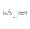
- FIG. 3 there is shown a cross-sectional representation of the manner in which the dopant material is mixed into the host material when the dopant material and host material undergo vaporization transfer and are deposited on the substrate.
- Host material layer 18 and dopant layer 20 are transferred and deposited on the substrate, forming transferred host material layer 72 , transferred dopant layer 76 , and mixed layer 74 .
- Mixed layer 74 is formed from the dopant layer 20 and host material layer 18 at interface 21 between the dopant and host materials.
- the mixing of dopant material and host material can be partial mixing or full mixing.
- OLED device 58 is formed on substrate 36 , which is coated in the region of interest with anode layer 60 .
- the conductive anode layer is formed over the substrate and, when EL emission is viewed through the anode, should be transparent or substantially transparent to the emission of interest.
- Common transparent anode materials used in this invention are indium-tin oxide and tin oxide, but other metal oxides can work including, but not limited to, aluminum- or indium-doped zinc oxide, magnesium-indium oxide, and nickel-tungsten oxide.
- metal nitrides such as gallium nitride, and metal selenides such as zinc selenide, and metal sulfides such as zinc sulfide, can be used as an anode material.
- the transmissive characteristics of the anode material are immaterial and any conductive material can be used, transparent, opaque or reflective.
- Example conductors for this application include, but are not limited to, gold, iridium, molybdenum, palladium, and platinum.
- Typical anode materials, transmissive or otherwise have a work function of 4.1 eV or greater. Desired anode materials can be deposited by any suitable means such as evaporation, sputtering, chemical vapor deposition, or electrochemical means.
- Anode materials can be patterned using well known photolithographic processes.
- OLED device 58 can further include hole-injecting layer 62 . While not always necessary, it is often useful that a hole-injecting layer be provided in an organic light-emitting display.
- the hole-injecting material can serve to improve the film formation property of subsequent organic layers and to facilitate injection of holes into the hole-transporting layer.
- Suitable materials for use in the hole-injecting layer include, but are not limited to, porphyrinic compounds as described in US-A-4,720,432, and plasma-deposited fluorocarbon polymers as described in US-A-6,208,075.
- Alternative hole-injecting materials reportedly useful in organic EL devices are described in EP 0 891 121 A1 and EP 1,029,909 Al.
- OLED device 58 further includes hole-transporting layer 64 .
- Hole-transport layer 64 can include any of the above-described hole-transporting materials. Desired hole-transporting materials can be deposited by any suitable means such as evaporation, sputtering, chemical vapor deposition, or electrochemical means. Hole-transporting materials can be patterned using well known photolithographic processes.
- OLED device 58 further includes emissive layer 66 , which can be deposited by the techniques of this invention.
- emissive layer 66 which can be deposited by the techniques of this invention.
- Useful organic emissive materials are well known.
- the light-emitting layer (LEL) of the organic EL element comprises a luminescent or fluorescent material where electroluminescence is produced as a result of electron-hole pair recombination in this region.
- the light-emitting layer can be comprised of a single material, but more commonly consists of a host material doped with a guest compound or compounds where light emission comes primarily from the dopant and can be of any color.
- the host materials in the light-emitting layer can be an electron-transporting material as previously described, a hole-transporting material as previously described, or another material that supports hole-electron recombination.
- the dopant material contained in the host material is as previously described.
- OLED device 58 further includes electron-transporting layer 68 .
- Desired electron-transporting materials can be deposited by any suitable means such as evaporation, sputtering, chemical vapor deposition, or electrochemical means. Electron-transporting materials can be patterned using well known photolithographic processes.
- Preferred electron-transporting materials for use in organic EL devices of this invention are metal chelated oxinoid compounds, including chelates of oxine itself (also commonly referred to as 8-quinolinol or 8-hydroxyquinoline). Such compounds help to inject and transport electrons and exhibit both high levels of performance and are readily fabricated in the form of thin films.
- Exemplary of contemplated oxinoid compounds are those satisfying structural Formula (G), previously described.
- electron-transporting materials include various butadiene derivatives as disclosed in US-A-4,356,429 and various heterocyclic optical brighteners as described in US-A-4,539,507.
- Benzazoles satisfying structural Formula (I) are also useful electron-transporting materials.
- electron-transporting materials can be polymeric substances, for example, polyphenylenevinylene derivatives, poly-para-phenylene derivatives, polyfluorene derivatives, polythiophenes, polyacetylenes, and other conductive polymeric organic materials such as those listed in Handbook of Conductive Molecules and Polymers, Vols. 1-4, H.S. Nalwa, ed., John Wiley and Sons, Chichester (1997).
- the OLED device 58 further includes cathode 70 .
- the cathode material can be comprised of nearly any conductive material. Desirable materials have good film-forming properties to ensure good contact with the underlying organic layer, promote electron injection at low voltage, and have good stability.
- Useful cathode materials often contain a low work function metal ( ⁇ 4.0 eV) or metal alloy.
- One preferred cathode material is comprised of a Mg:Ag alloy wherein the percentage of silver is in the range of 1 to 20 %, as described in US-A-4,885,221.
- Another suitable class of cathode materials includes bilayers comprised of a thin layer of a low work function metal or metal salt capped with a thicker layer of conductive metal.
- cathode is comprised of a thin layer of LiF followed by a thicker layer of A1 as described in US-A-5,677,572.
- Other useful cathode materials include, but are not limited to, those disclosed in US-A-5,059,861; US-A-5,059,862; and US-A-6,140,763.
- the cathode When light emission is viewed through the cathode, the cathode must be transparent or nearly transparent. For such applications, metals must be thin or one must use transparent conductive oxides, or a combination of these materials.
- Optically transparent cathodes have been described in more detail in US-A-5,776,623. Cathode materials can be deposited by evaporation, sputtering, or chemical vapor deposition. When needed, patterning can be achieved through many well known methods including, but not limited to, through-mask deposition, integral shadow masking as described in US-A-5,276,380 and EP 0 732 868, laser transfer, and selective chemical vapor deposition.
- FIG. 5 referring also to FIG. 2a and 2b, there is shown a plan view of treated substrate 82, which has been treated in the manner described in this invention.
- Predetermined portions of organic material 30 have been transferred to substrate 36 in transferred pattern 80 .
- Transferred pattern 80 has been formed in a manner consistent with the end-use of treated substrate 82 (for example, transferred pattern 80 is of an OLED light-emissive material that has been transferred to the positions of existing thin-film transistors on substrate 36 ).
- Transferred pattern 80 reflects the method used to prepare it (for example, radiation-absorbing material 22 in a patterned layer in FIG. 2b or the pattern of laser light 48 irradiation in FIG. 2a).
- a donor element satisfying the requirements of the invention was constructed in the following manner:
- An OLED device satisfying the requirements of the invention was constructed in the following manner:
- a comparative donor element was constructed in the manner described for donor element Example 1, except in step 2, 20 nm of TBADN and 0.25 nm of TBP were vacuum codeposited onto the chromium layer to form a mixed donor.
- a comparative OLED device was constructed in the manner described for OLED device Example 1, except the donor element prepared in donor element example 2 was used in step 4.
- a comparative OLED device was constructed in the manner described for OLED device Example 1, except that step 4 was as follows: 4. A layer of 0.25 nm of TBP was vacuum deposited onto the NPB layer, followed by a second layer of 20 nm TBADN.
- a comparative OLED device was constructed in the manner described for OLED device Example 3 except in step 4, 20 nm of TBADN and 0.25 nm of TBP were vacuum codeposited onto the NPB layer to form a mixed layer.
- Example # Example Type CIE X CIE Y Luminance at 20 mA/cm 2 (cd/m 2 ) Dopant Emission? 1 invention 0.159 0.210 314 Yes 2 Donor control 0.159 0.209 350 Yes 3 Double-layer control 0.163 0.124 252 Minimal 4 Mixed-layer control 0.162 0.216 358 Yes
- a donor element satisfying the requirements of the invention was constructed in the manner described for donor element Example 1, except step 2 was as follows: 2.
- a layer of 20 nm of ALQ was vacuum deposited onto the chromium layer, followed by a second layer of 0.4 nm of 4-(dicyanomethylene)-2-t-butyl-6-(1,1,7,7-tetramethyljulolidyl-9-enyl)-4H-pyran (DCJTB).
- An OLED device satisfying the requirements of the invention was constructed in the manner described for OLED device Example 1, except in step 4 the donor element prepared in donor element Example 3 was used, and a gap of 75 microns was maintained by the use of a metal shim spacer between the donor element and the OLED substrate.
- a comparative donor element was constructed in the manner described for donor element Example 3, except in step 2, 20 nm of ALQ and 0.4 nm of DCJTB were vacuum codeposited onto the chromium layer to form a mixed donor.
- a comparative OLED device was constructed in the manner described for OLED device Example 5, except the donor element prepared in donor element example 4 was used in step 4.
- a comparative OLED device was constructed in the manner described for OLED device Example 1, except that step 4 was as follows: 4. A layer of 0.4 nm of DCJTB was vacuum deposited onto the NPB layer, followed by a second layer of 20 nm ALQ.
- a comparative OLED device was constructed in the manner described for OLED device Example 7 except in step 4, 20 nm of ALQ and 0.4 nm of DCJTB were vacuum codeposited onto the NPB layer to form a mixed layer.
- Example # Example Type CIE X CIE Y Luminance at 20 mA/cm 2 (cd/m 2 ) Dopant Emission? 5 invention 0.58 0.40 300 Yes 6 Donor control 0.63 0.37 192 Yes 7 Double-layer control 0.42 0.51 157 Some 8 Mixed-layer control 0.64 0.36 319 Yes
- the method wherein the light is provided by a laser source.
- the method wherein the laser light is from an infrared laser.
- the method further including providing a reduced pressure atmosphere in the gap between the donor element and the OLED substrate.
Landscapes
- Chemical & Material Sciences (AREA)
- Engineering & Computer Science (AREA)
- Organic Chemistry (AREA)
- Materials Engineering (AREA)
- Mechanical Engineering (AREA)
- Chemical Kinetics & Catalysis (AREA)
- Metallurgy (AREA)
- Manufacturing & Machinery (AREA)
- Health & Medical Sciences (AREA)
- Toxicology (AREA)
- Physics & Mathematics (AREA)
- Optics & Photonics (AREA)
- Electroluminescent Light Sources (AREA)
Applications Claiming Priority (2)
| Application Number | Priority Date | Filing Date | Title |
|---|---|---|---|
| US10/210,934 US6939660B2 (en) | 2002-08-02 | 2002-08-02 | Laser thermal transfer donor including a separate dopant layer |
| US210934 | 2002-08-02 |
Publications (2)
| Publication Number | Publication Date |
|---|---|
| EP1426189A2 true EP1426189A2 (de) | 2004-06-09 |
| EP1426189A3 EP1426189A3 (de) | 2005-12-28 |
Family
ID=31494285
Family Applications (1)
| Application Number | Title | Priority Date | Filing Date |
|---|---|---|---|
| EP03077293A Withdrawn EP1426189A3 (de) | 2002-08-02 | 2003-07-21 | Thermisches Übertragungselement für den Transfer durch Laser mit eigener Dotierschicht |
Country Status (6)
| Country | Link |
|---|---|
| US (1) | US6939660B2 (de) |
| EP (1) | EP1426189A3 (de) |
| JP (1) | JP4437018B2 (de) |
| KR (1) | KR101004058B1 (de) |
| CN (1) | CN1310772C (de) |
| TW (1) | TWI277368B (de) |
Cited By (1)
| Publication number | Priority date | Publication date | Assignee | Title |
|---|---|---|---|---|
| US8551557B2 (en) | 2007-07-06 | 2013-10-08 | Semiconductor Energy Laboratory Co., Ltd. | Method for manufacturing light-emitting device |
Families Citing this family (19)
| Publication number | Priority date | Publication date | Assignee | Title |
|---|---|---|---|---|
| JP4197447B2 (ja) * | 2003-03-31 | 2008-12-17 | 富士フイルム株式会社 | 有機電界発光素子の製造方法及びその有機電界発光素子 |
| US20050145326A1 (en) * | 2004-01-05 | 2005-07-07 | Eastman Kodak Company | Method of making an OLED device |
| US20050181141A1 (en) * | 2004-02-18 | 2005-08-18 | Aiden Flanagan | Laser-induced explosive vaporization coating method, associated system, and device made by the method |
| WO2005122158A1 (en) * | 2004-06-11 | 2005-12-22 | Koninklijke Philips Electronics N.V. | Improved information carrier |
| JP2006057173A (ja) * | 2004-08-24 | 2006-03-02 | Tohoku Pioneer Corp | 成膜源、真空成膜装置、有機elパネルの製造方法 |
| KR100721565B1 (ko) | 2004-11-17 | 2007-05-23 | 삼성에스디아이 주식회사 | 저분자 유기 전계 발광 소자 및 그의 제조 방법 |
| US7268006B2 (en) * | 2004-12-30 | 2007-09-11 | E.I. Du Pont De Nemours And Company | Electronic device including a guest material within a layer and a process for forming the same |
| US7630029B2 (en) * | 2005-02-16 | 2009-12-08 | Industrial Technology Research Institute | Conductive absorption layer for flexible displays |
| US7648741B2 (en) * | 2005-05-17 | 2010-01-19 | Eastman Kodak Company | Forming a patterned metal layer using laser induced thermal transfer method |
| US7781023B2 (en) * | 2005-10-11 | 2010-08-24 | Hewlett-Packard Development Company, L.P. | Method of producing an electroluminescent display |
| US20070080632A1 (en) * | 2005-10-11 | 2007-04-12 | Lambright Terry M | Electroluminescent display system |
| JP2009048811A (ja) | 2007-08-16 | 2009-03-05 | Sony Corp | 転写用基板および有機電界発光素子の製造方法 |
| JP5416987B2 (ja) * | 2008-02-29 | 2014-02-12 | 株式会社半導体エネルギー研究所 | 成膜方法及び発光装置の作製方法 |
| JP5079722B2 (ja) | 2008-03-07 | 2012-11-21 | 株式会社半導体エネルギー研究所 | 発光装置の作製方法 |
| JP5317906B2 (ja) * | 2009-09-23 | 2013-10-16 | 株式会社半導体エネルギー研究所 | 成膜方法 |
| EP2731126A1 (de) | 2012-11-09 | 2014-05-14 | Nederlandse Organisatie voor toegepast -natuurwetenschappelijk onderzoek TNO | Verfahren zum Binden von Chipfarbstoffen |
| KR20180030609A (ko) * | 2015-07-09 | 2018-03-23 | 오르보테크 엘티디. | Lift 토출 각도의 제어 |
| DE102015119327A1 (de) * | 2015-11-10 | 2017-05-11 | Von Ardenne Gmbh | Verfahren, Beschichtungsanordnung und Beschichtungsmaterial-Transfer-Maske |
| KR102935478B1 (ko) * | 2020-12-08 | 2026-03-10 | 삼성디스플레이 주식회사 | 발광 소자 및 발광 소자용 아민 화합물 |
Family Cites Families (50)
| Publication number | Priority date | Publication date | Assignee | Title |
|---|---|---|---|---|
| NL250330A (de) * | 1959-04-09 | |||
| US3658520A (en) * | 1968-02-20 | 1972-04-25 | Eastman Kodak Co | Photoconductive elements containing as photoconductors triarylamines substituted by active hydrogen-containing groups |
| US3567450A (en) * | 1968-02-20 | 1971-03-02 | Eastman Kodak Co | Photoconductive elements containing substituted triarylamine photoconductors |
| US4356429A (en) * | 1980-07-17 | 1982-10-26 | Eastman Kodak Company | Organic electroluminescent cell |
| US4539507A (en) * | 1983-03-25 | 1985-09-03 | Eastman Kodak Company | Organic electroluminescent devices having improved power conversion efficiencies |
| DE3518323A1 (de) * | 1985-05-22 | 1986-11-27 | SEVAR Entsorgungsanlagen GmbH, 8590 Marktredwitz | Verfahren und vorrichtung zum trocknen von klaerschlamm |
| US4885221A (en) * | 1986-12-06 | 1989-12-05 | Kabushiki Kaisha Toshiba | Electrophotography apparatus and electrophtographic process for developing positive image from positive or negative film |
| US4720432A (en) * | 1987-02-11 | 1988-01-19 | Eastman Kodak Company | Electroluminescent device with organic luminescent medium |
| US4769292A (en) * | 1987-03-02 | 1988-09-06 | Eastman Kodak Company | Electroluminescent device with modified thin film luminescent zone |
| US4772582A (en) * | 1987-12-21 | 1988-09-20 | Eastman Kodak Company | Spacer bead layer for dye-donor element used in laser-induced thermal dye transfer |
| US5061569A (en) * | 1990-07-26 | 1991-10-29 | Eastman Kodak Company | Electroluminescent device with organic electroluminescent medium |
| US5059861A (en) * | 1990-07-26 | 1991-10-22 | Eastman Kodak Company | Organic electroluminescent device with stabilizing cathode capping layer |
| US5059862A (en) * | 1990-07-26 | 1991-10-22 | Eastman Kodak Company | Electroluminescent device with improved cathode |
| US5141671A (en) * | 1991-08-01 | 1992-08-25 | Eastman Kodak Company | Mixed ligand 8-quinolinolato aluminum chelate luminophors |
| US5151629A (en) * | 1991-08-01 | 1992-09-29 | Eastman Kodak Company | Blue emitting internal junction organic electroluminescent device (I) |
| US5150006A (en) * | 1991-08-01 | 1992-09-22 | Eastman Kodak Company | Blue emitting internal junction organic electroluminescent device (II) |
| US5294870A (en) * | 1991-12-30 | 1994-03-15 | Eastman Kodak Company | Organic electroluminescent multicolor image display device |
| DE69305262T2 (de) * | 1992-07-13 | 1997-04-30 | Eastman Kodak Co | Einen inneren Übergang aufweisende organisch elektrolumineszierende Vorrichtung mit einer neuen Zusammensetzung |
| US5405709A (en) * | 1993-09-13 | 1995-04-11 | Eastman Kodak Company | White light emitting internal junction organic electroluminescent device |
| JP3813217B2 (ja) | 1995-03-13 | 2006-08-23 | パイオニア株式会社 | 有機エレクトロルミネッセンスディスプレイパネルの製造方法 |
| JP3401356B2 (ja) * | 1995-02-21 | 2003-04-28 | パイオニア株式会社 | 有機エレクトロルミネッセンスディスプレイパネルとその製造方法 |
| US5593788A (en) * | 1996-04-25 | 1997-01-14 | Eastman Kodak Company | Organic electroluminescent devices with high operational stability |
| US5688551A (en) * | 1995-11-13 | 1997-11-18 | Eastman Kodak Company | Method of forming an organic electroluminescent display panel |
| US5578416A (en) * | 1995-11-20 | 1996-11-26 | Eastman Kodak Company | Cinnamal-nitrile dyes for laser recording element |
| US5683823A (en) * | 1996-01-26 | 1997-11-04 | Eastman Kodak Company | White light-emitting organic electroluminescent devices |
| US5776623A (en) * | 1996-07-29 | 1998-07-07 | Eastman Kodak Company | Transparent electron-injecting electrode for use in an electroluminescent device |
| US5677572A (en) * | 1996-07-29 | 1997-10-14 | Eastman Kodak Company | Bilayer electrode on a n-type semiconductor |
| US5645948A (en) * | 1996-08-20 | 1997-07-08 | Eastman Kodak Company | Blue organic electroluminescent devices |
| EP0891121B8 (de) | 1996-12-28 | 2013-01-02 | Futaba Corporation | Organische elektrolumineszente elementen |
| US5935720A (en) * | 1997-04-07 | 1999-08-10 | Eastman Kodak Company | Red organic electroluminescent devices |
| US5755999A (en) * | 1997-05-16 | 1998-05-26 | Eastman Kodak Company | Blue luminescent materials for organic electroluminescent devices |
| US5928802A (en) * | 1997-05-16 | 1999-07-27 | Eastman Kodak Company | Efficient blue organic electroluminescent devices |
| GB9711237D0 (en) | 1997-06-02 | 1997-07-23 | Isis Innovation | Organomettallic Complexes |
| US5937272A (en) * | 1997-06-06 | 1999-08-10 | Eastman Kodak Company | Patterned organic layers in a full-color organic electroluminescent display array on a thin film transistor array substrate |
| US5851709A (en) * | 1997-10-31 | 1998-12-22 | Eastman Kodak Company | Method for selective transfer of a color organic layer |
| US5935721A (en) * | 1998-03-20 | 1999-08-10 | Eastman Kodak Company | Organic electroluminescent elements for stable electroluminescent |
| US6140763A (en) * | 1998-07-28 | 2000-10-31 | Eastman Kodak Company | Interfacial electron-injecting layer formed from a doped cathode for organic light-emitting structure |
| CN1213127C (zh) | 1998-09-09 | 2005-08-03 | 出光兴产株式会社 | 有机电致发光器件与苯二胺衍生物 |
| GB9820805D0 (en) | 1998-09-25 | 1998-11-18 | Isis Innovation | Divalent lanthanide metal complexes |
| US6208075B1 (en) * | 1998-11-05 | 2001-03-27 | Eastman Kodak Company | Conductive fluorocarbon polymer and method of making same |
| US6048573A (en) * | 1998-11-13 | 2000-04-11 | Eastman Kodak Company | Method of making an organic light-emitting device |
| US6361886B2 (en) | 1998-12-09 | 2002-03-26 | Eastman Kodak Company | Electroluminescent device with improved hole transport layer |
| US6020078A (en) * | 1998-12-18 | 2000-02-01 | Eastman Kodak Company | Green organic electroluminescent devices |
| EP1144197B1 (de) * | 1999-01-15 | 2003-06-11 | 3M Innovative Properties Company | Thermisches Übertragungsverfahren. |
| US6114088A (en) * | 1999-01-15 | 2000-09-05 | 3M Innovative Properties Company | Thermal transfer element for forming multilayer devices |
| KR101166264B1 (ko) | 1999-03-23 | 2012-07-17 | 유니버시티 오브 서던 캘리포니아 | 유기 엘이디의 인광성 도펀트로서의 사이클로메탈화 금속복합체 |
| KR100913568B1 (ko) | 1999-05-13 | 2009-08-26 | 더 트러스티즈 오브 프린스턴 유니버시티 | 전계인광에 기초한 고 효율의 유기 발광장치 |
| SG118110A1 (en) * | 2001-02-01 | 2006-01-27 | Semiconductor Energy Lab | Organic light emitting element and display device using the element |
| US6555284B1 (en) * | 2001-12-27 | 2003-04-29 | Eastman Kodak Company | In situ vacuum method for making OLED devices |
| US6610455B1 (en) * | 2002-01-30 | 2003-08-26 | Eastman Kodak Company | Making electroluminscent display devices |
-
2002
- 2002-08-02 US US10/210,934 patent/US6939660B2/en not_active Expired - Lifetime
-
2003
- 2003-06-17 TW TW092116382A patent/TWI277368B/zh not_active IP Right Cessation
- 2003-07-21 EP EP03077293A patent/EP1426189A3/de not_active Withdrawn
- 2003-08-01 CN CNB03152527XA patent/CN1310772C/zh not_active Expired - Lifetime
- 2003-08-01 JP JP2003205330A patent/JP4437018B2/ja not_active Expired - Lifetime
- 2003-08-02 KR KR1020030053606A patent/KR101004058B1/ko not_active Expired - Lifetime
Cited By (1)
| Publication number | Priority date | Publication date | Assignee | Title |
|---|---|---|---|---|
| US8551557B2 (en) | 2007-07-06 | 2013-10-08 | Semiconductor Energy Laboratory Co., Ltd. | Method for manufacturing light-emitting device |
Also Published As
| Publication number | Publication date |
|---|---|
| EP1426189A3 (de) | 2005-12-28 |
| US6939660B2 (en) | 2005-09-06 |
| KR101004058B1 (ko) | 2010-12-27 |
| TW200408310A (en) | 2004-05-16 |
| KR20040012609A (ko) | 2004-02-11 |
| US20040029039A1 (en) | 2004-02-12 |
| CN1310772C (zh) | 2007-04-18 |
| JP2004071550A (ja) | 2004-03-04 |
| CN1480342A (zh) | 2004-03-10 |
| TWI277368B (en) | 2007-03-21 |
| JP4437018B2 (ja) | 2010-03-24 |
Similar Documents
| Publication | Publication Date | Title |
|---|---|---|
| US6610455B1 (en) | Making electroluminscent display devices | |
| US6890627B2 (en) | Laser thermal transfer from a donor element containing a hole-transporting layer | |
| US7052351B2 (en) | Using hole- or electron-blocking layers in color OLEDS | |
| EP1324404B1 (de) | In-situ Vakuumverfahren zur Herstellung von OLED Vorrichtungen | |
| US6939660B2 (en) | Laser thermal transfer donor including a separate dopant layer | |
| EP1333510A2 (de) | Verwendung von Abstandhaltern für Herstellung von elektrolumineszierenden Anzeigevorrichtungen | |
| US6703180B1 (en) | Forming an improved stability emissive layer from a donor element in an OLED device | |
| US20050145326A1 (en) | Method of making an OLED device | |
| US20040151829A1 (en) | Optimizing OLED emission | |
| US6824950B2 (en) | Forming an oled device with a performance-inhancing layer | |
| EP1475850A2 (de) | Emissionsschutzschicht in einer organischen Leuchtdiode | |
| EP1408564A2 (de) | Abstandskontrolle während des laserunterstützten Thermotransfers bei der OLED-Herstellung | |
| US7485337B2 (en) | Depositing an organic layer for use in OLEDs | |
| US7132140B2 (en) | Plural metallic layers in OLED donor | |
| US6781149B1 (en) | OLED device with a performance-enhancing layer |
Legal Events
| Date | Code | Title | Description |
|---|---|---|---|
| PUAI | Public reference made under article 153(3) epc to a published international application that has entered the european phase |
Free format text: ORIGINAL CODE: 0009012 |
|
| AK | Designated contracting states |
Kind code of ref document: A2 Designated state(s): AT BE BG CH CY CZ DE DK EE ES FI FR GB GR HU IE IT LI LU MC NL PT RO SE SI SK TR |
|
| AX | Request for extension of the european patent |
Extension state: AL LT LV MK |
|
| PUAL | Search report despatched |
Free format text: ORIGINAL CODE: 0009013 |
|
| AK | Designated contracting states |
Kind code of ref document: A3 Designated state(s): AT BE BG CH CY CZ DE DK EE ES FI FR GB GR HU IE IT LI LU MC NL PT RO SE SI SK TR |
|
| AX | Request for extension of the european patent |
Extension state: AL LT LV MK |
|
| RIC1 | Information provided on ipc code assigned before grant |
Ipc: 7B 41J 2/435 B Ipc: 7H 01L 51/40 A |
|
| AKX | Designation fees paid | ||
| REG | Reference to a national code |
Ref country code: DE Ref legal event code: 8566 |
|
| STAA | Information on the status of an ep patent application or granted ep patent |
Free format text: STATUS: THE APPLICATION IS DEEMED TO BE WITHDRAWN |
|
| 18D | Application deemed to be withdrawn |
Effective date: 20060629 |