EP1426462A2 - Procédé et appareillage de déposition en phase vapeur utilisant un masque, masque, procédé de fabrication d'un panneau d'affichage, panneau d'affichage et appareil électronique - Google Patents
Procédé et appareillage de déposition en phase vapeur utilisant un masque, masque, procédé de fabrication d'un panneau d'affichage, panneau d'affichage et appareil électronique Download PDFInfo
- Publication number
- EP1426462A2 EP1426462A2 EP03027352A EP03027352A EP1426462A2 EP 1426462 A2 EP1426462 A2 EP 1426462A2 EP 03027352 A EP03027352 A EP 03027352A EP 03027352 A EP03027352 A EP 03027352A EP 1426462 A2 EP1426462 A2 EP 1426462A2
- Authority
- EP
- European Patent Office
- Prior art keywords
- deposition
- mask
- subject
- glass substrate
- substrate
- Prior art date
- Legal status (The legal status is an assumption and is not a legal conclusion. Google has not performed a legal analysis and makes no representation as to the accuracy of the status listed.)
- Withdrawn
Links
Images


Classifications
-
- C—CHEMISTRY; METALLURGY
- C23—COATING METALLIC MATERIAL; COATING MATERIAL WITH METALLIC MATERIAL; CHEMICAL SURFACE TREATMENT; DIFFUSION TREATMENT OF METALLIC MATERIAL; COATING BY VACUUM EVAPORATION, BY SPUTTERING, BY ION IMPLANTATION OR BY CHEMICAL VAPOUR DEPOSITION, IN GENERAL; INHIBITING CORROSION OF METALLIC MATERIAL OR INCRUSTATION IN GENERAL
- C23C—COATING METALLIC MATERIAL; COATING MATERIAL WITH METALLIC MATERIAL; SURFACE TREATMENT OF METALLIC MATERIAL BY DIFFUSION INTO THE SURFACE, BY CHEMICAL CONVERSION OR SUBSTITUTION; COATING BY VACUUM EVAPORATION, BY SPUTTERING, BY ION IMPLANTATION OR BY CHEMICAL VAPOUR DEPOSITION, IN GENERAL
- C23C14/00—Coating by vacuum evaporation, by sputtering or by ion implantation of the coating forming material
- C23C14/22—Coating by vacuum evaporation, by sputtering or by ion implantation of the coating forming material characterised by the process of coating
- C23C14/24—Vacuum evaporation
-
- G—PHYSICS
- G02—OPTICS
- G02F—OPTICAL DEVICES OR ARRANGEMENTS FOR THE CONTROL OF LIGHT BY MODIFICATION OF THE OPTICAL PROPERTIES OF THE MEDIA OF THE ELEMENTS INVOLVED THEREIN; NON-LINEAR OPTICS; FREQUENCY-CHANGING OF LIGHT; OPTICAL LOGIC ELEMENTS; OPTICAL ANALOGUE/DIGITAL CONVERTERS
- G02F1/00—Devices or arrangements for the control of the intensity, colour, phase, polarisation or direction of light arriving from an independent light source, e.g. switching, gating or modulating; Non-linear optics
- G02F1/01—Devices or arrangements for the control of the intensity, colour, phase, polarisation or direction of light arriving from an independent light source, e.g. switching, gating or modulating; Non-linear optics for the control of the intensity, phase, polarisation or colour
- G02F1/13—Devices or arrangements for the control of the intensity, colour, phase, polarisation or direction of light arriving from an independent light source, e.g. switching, gating or modulating; Non-linear optics for the control of the intensity, phase, polarisation or colour based on liquid crystals, e.g. single liquid crystal display cells
-
- C—CHEMISTRY; METALLURGY
- C23—COATING METALLIC MATERIAL; COATING MATERIAL WITH METALLIC MATERIAL; CHEMICAL SURFACE TREATMENT; DIFFUSION TREATMENT OF METALLIC MATERIAL; COATING BY VACUUM EVAPORATION, BY SPUTTERING, BY ION IMPLANTATION OR BY CHEMICAL VAPOUR DEPOSITION, IN GENERAL; INHIBITING CORROSION OF METALLIC MATERIAL OR INCRUSTATION IN GENERAL
- C23C—COATING METALLIC MATERIAL; COATING MATERIAL WITH METALLIC MATERIAL; SURFACE TREATMENT OF METALLIC MATERIAL BY DIFFUSION INTO THE SURFACE, BY CHEMICAL CONVERSION OR SUBSTITUTION; COATING BY VACUUM EVAPORATION, BY SPUTTERING, BY ION IMPLANTATION OR BY CHEMICAL VAPOUR DEPOSITION, IN GENERAL
- C23C14/00—Coating by vacuum evaporation, by sputtering or by ion implantation of the coating forming material
- C23C14/04—Coating on selected surface areas, e.g. using masks
- C23C14/042—Coating on selected surface areas, e.g. using masks using masks
-
- C—CHEMISTRY; METALLURGY
- C09—DYES; PAINTS; POLISHES; NATURAL RESINS; ADHESIVES; COMPOSITIONS NOT OTHERWISE PROVIDED FOR; APPLICATIONS OF MATERIALS NOT OTHERWISE PROVIDED FOR
- C09K—MATERIALS FOR MISCELLANEOUS APPLICATIONS, NOT PROVIDED FOR ELSEWHERE
- C09K2323/00—Functional layers of liquid crystal optical display excluding electroactive liquid crystal layer characterised by chemical composition
-
- G—PHYSICS
- G03—PHOTOGRAPHY; CINEMATOGRAPHY; ANALOGOUS TECHNIQUES USING WAVES OTHER THAN OPTICAL WAVES; ELECTROGRAPHY; HOLOGRAPHY
- G03F—PHOTOMECHANICAL PRODUCTION OF TEXTURED OR PATTERNED SURFACES, e.g. FOR PRINTING, FOR PROCESSING OF SEMICONDUCTOR DEVICES; MATERIALS THEREFOR; ORIGINALS THEREFOR; APPARATUS SPECIALLY ADAPTED THEREFOR
- G03F9/00—Registration or positioning of originals, masks, frames, photographic sheets or textured or patterned surfaces, e.g. automatically
Definitions
- the present invention relates to a mask vapor deposition method in which a masking operation is performed and vacuum deposition is then performed and also relates to a mask vapor deposition system, a mask used for vapor deposition and the like, an apparatus for manufacturing a display panel, a display panel, and an electronic device.
- a vapor deposition method has been used for forming thin-films on, for example, substrates using deposition materials.
- vapor deposition is performed in such a manner that a mask for vapor deposition (hereinafter referred to as a deposition mask) covers a surface so as to protect areas, on which thin-films or the like are not formed, against the vapor deposition.
- the deposition mask must be placed so as not to be displaced.
- EL elements electroluminescent elements
- the deposited compounds directly emit light and therefore the compounds must be each deposited on corresponding predetermined areas in a precise manner depending on display colors so as not to disturb balance.
- the mask must have high definition.
- a display panel including such EL elements compounds for emitting light are deposited on a glass substrate, which is a subject for deposition.
- the glass substrate is warped due to film formation, ion implantation, and heat treatment for forming various thin-films such as TFDs (Thin Film Diodes) and TFTs (Thin Film transistors) in some cases.
- TFDs Thin Film Diodes
- TFTs Thin Film transistors
- the deposition mask Since the deposition mask is usually aligned with the glass substrate using alignment marks placed on end portions having no bearing on the display panel, the fact that the warp is increased at the center means that the distance between the alignment marks placed on the deposition mask and the glass substrate is increased. Since the alignment is performed based on an obtained image, there is a problem in that an increase in distance therebetween causes defocusing. Therefore, the preciseness of the alignment is lowered and a great deal of time is involved in repeating the alignment. Thus, even if the mask has high definition, deposition cannot be performed with high preciseness and a great deal of time is spent. This problem is not characteristic of the glass substrate but is in common with other subjects for deposition.
- a mask that has a thickness of 0.05 mm and contains ferromagnetic metal is prepared so as to allow the mask to adhere to a warped glass substrate, and the mask is securely joined to the substrate by attracting the mask using a permanent magnet placed on the back face of the substrate while the mask follows the warp of the substrate (see, for example, Patent Document 1).
- the mask is aligned with the substrate and the resulting mask is then securely joined to the substrate by attracting the mask using the permanent magnet. Therefore, a misalignment between the mask and substrate is caused by shock due to the collision of the permanent magnet with the substrate in some cases.
- the deposition mask is heated by radiant heat generated by heating a deposition material, whereby the mask is expanded in some cases.
- the deposition mask must contain metal (for example, nickel alloy or the like) attracted by a magnet in particular.
- the mask is warped or bent due to thermal stress, whereby the adhesion between the mask and the substrate is lowered and the mask is released from the substrate in some cases.
- the mask cannot be continuously used.
- the adhesion is insufficient, the deposition material sticks onto shadow areas and is therefore deposited on the areas, on which the deposition material must not be deposited, in some cases.
- the above method is not fit for the manufacture of large-sized products and mass-production.
- processing accuracy in preparing metal masks is insufficient to prepare a high-definition mask for manufacturing panels including EL elements.
- a mask vapor deposition method includes a step of attracting a subject for deposition using electrostatic attraction, a step of aligning the attracted deposition subject with a deposition mask, and a step of evaporating a deposition material to deposit the material on the deposition subject.
- the deposition subject is attracted by electrostatic chucking or the like and retained while the warp is corrected, the attracted deposition subject is aligned with the deposition mask, and the deposition material is deposited on the deposition subject according to the pattern of the deposition mask.
- the warp of the deposition subject is corrected; hence, the adhesion of the deposition mask is increased, and the deposition material is prevented from sticking onto shadow areas during the vapor deposition, whereby the vapor deposition can be precisely performed.
- the deposition mask can be prepared using a material such as silicon that is not attracted by a magnet. In the steps, since shock and the like are not generated after the completion of alignment, the vapor deposition can be performed while the precise alignment is maintained.
- a mask vapor deposition method includes a step of aligning a subject for deposition with a vapor deposition mask having an electrostatic chucking function, a step of attracting the deposition subject to the deposition mask using electrostatic attraction, and a step of evaporating a deposition material to deposit the material on the deposition subject.
- the vapor deposition mask has the electrostatic chucking function.
- the deposition mask is aligned with the deposition subject, the deposition subject is attracted by the electrostatic attraction and retained while the warp of the deposition subject is corrected, and the deposition material is then deposited. Since the deposition mask that can attract the deposition subject using the electrostatic chucking or the like is used, the adhesion between the deposition mask and the deposition subject can be greatly increased. Therefore, the deposition material is prevented from sticking onto shadow areas during the vapor deposition, whereby the vapor deposition can be precisely performed.
- a mask vapor deposition system includes an electrostatic chucking mechanism for attracting a subject for deposition using electrostatic attraction; a deposition mask, brought into close contact with a face of the deposition subject, for depositing a deposition material in a predetermined pattern, the face being reverse to that of the deposition subject attracted by the electrostatic chucking mechanism; an evaporation source for evaporating the deposition material; and a vacuum chamber, wherein the mechanism, mask, and source are at least placed in the vacuum chamber.
- the electrostatic chucking mechanism attracts the deposition subject using electrostatic attraction and retains the deposition subject while the warp is corrected, the deposition mask is brought into close contact with a face of the deposition subject which is reverse to a face attracted by the mechanism, and the deposition material is evaporated from the deposition source, thereby performing vapor deposition according to the pattern of the deposition mask.
- the warp of the deposition subject is corrected; hence, the adhesion of the deposition mask is increased, and the deposition material is prevented from sticking onto shadow areas during the vapor deposition, whereby the vapor deposition can be precisely performed.
- the deposition mask can be prepared using a material such as silicon that is not attracted by a magnet.
- the steps since shock and the like are not generated after the completion of alignment, the vapor deposition can be performed while the precise alignment is maintained.
- the mask vapor deposition system of the present invention further includes a ferromagnetic means for bringing the deposition subject into close contact with the deposition mask prepared using a magnetic material.
- the system in order to increase the adhesion when the deposition mask is made of metal and is therefore attracted by magnetic force, the system further includes the ferromagnetic means such as an electromagnet.
- the ferromagnetic means such as an electromagnet.
- a mask vapor deposition system includes a deposition mask for attracting a subject for deposition using electrostatic attraction and depositing a deposition material on the deposition subject in a predetermined pattern, an evaporation source for evaporating the deposition material, and a vacuum chamber, wherein the mask and source are at least placed in the vacuum chamber.
- the deposition mask has an electrostatic chucking function. The deposition mask is aligned with the deposition subject, the deposition subject is attracted by electrostatic attraction and retained while the warp of the deposition subject is corrected, and the deposition material is evaporated from the deposition source, thereby performing vapor deposition according to a pattern.
- the deposition mask that can attract the deposition subject using electrostatic chucking or the like since the deposition mask that can attract the deposition subject using electrostatic chucking or the like is used, the adhesion between the deposition mask and the deposition subject can be greatly increased. Therefore, the deposition material is prevented from sticking onto shadow areas during the vapor deposition, whereby the vapor deposition can be precisely performed.
- a process for manufacturing a deposition mask according to the present invention includes a step of forming an insulating layer on a semiconductor substrate; a step of providing a metal layer functioning as electrodes, on a predetermined portion of the insulating layer; a step of forming perforations for deposition in predetermined areas of the semiconductor substrate; and a step of further forming another insulating layer on the metal layer.
- one insulating layer is formed on the semiconductor substrate and the metal layer functioning as electrodes for performing electrostatic chucking is then formed. After the perforations constituting a mask pattern are formed, the other insulating layer is formed in order to insulate the deposition mask from a subject for deposition.
- the perforations that are hardly deformed by heat can be formed with high precision by a precise processing method such as an etching method and the mask having high flatness can be obtained.
- the mask that can increase the adhesion of the deposition subject using electrostatic chucking can be manufactured.
- a deposition mask according to the present invention includes a semiconductor substrate having perforations for deposition in predetermined areas of the substrate, wherein the deposition mask attracts a subject for deposition using electrostatic attraction by supplying electric charges.
- the mask which is not a metal mask, includes a semiconductor substrate made of, for example, gallium arsenic (GaAs) or the like and has perforations formed by an etching method according to the pattern of the deposition.
- the deposition mask of the present invention has an electrostatic chucking function and attracts the deposition subject using electrostatic attraction.
- the perforations that are hardly deformed by heat can be formed with high precision by a precise processing method such as an etching method and the mask having high flatness can be obtained.
- the adhesion between the deposition mask and deposition subject can be increased by electrostatic chucking.
- a deposition mask according to the present invention includes a wired substrate and a single semiconductor substrate or a plurality of semiconductor substrates having perforations for deposition, in predetermined areas of the substrate, wherein the semiconductor substrate or semiconductor substrates are bonded to the wired substrate so as to function as electrodes for attracting a subject for deposition using electrostatic attraction.
- the semiconductor substrate or semiconductor substrates having the perforations formed by, for example, an etching method according to the pattern of deposition are prepared and then bonded to the wired substrate.
- the semiconductor substrate or semiconductor substrates are used as masks and also used as electrodes.
- the perforations that are hardly deformed by heat can be formed with high precision by a precise processing method such as an etching method and the deposition mask having high flatness can be obtained.
- the adhesion between the deposition mask and deposition subject can be increased by electrostatic chucking.
- the semiconductor substrate or semiconductor substrates are made of silicon.
- silicon (Si) is used as a material for the mask.
- the mask can be processed with high precision by an etching method or the like.
- the mask can be used as electrodes.
- the deposition mask according to the present invention further includes electrodes having a positive or a negative polarity alternately arranged on the semiconductor substrate.
- the positive and negative electrodes are alternately arranged on the semiconductor substrate.
- a bipolar electrostatic chuck can be achieved using the mask.
- the electrodes are arranged so as to form an interdigital pattern.
- the positive and negative electrodes are arranged so as to form an interdigital pattern densely.
- the deposition mask of the present invention a portion of the mask to be brought into contact with the subject for deposition is covered with silicon dioxide.
- the portion to be brought into contact with the deposition subject is covered with silicon dioxide.
- An apparatus for manufacturing a display panel includes an electrostatic chucking mechanism for attracting a glass substrate that is a subject for deposition using electrostatic attraction; a deposition mask to be brought into close contact with a face of the glass substrate in order to deposit an organic material, which is used for forming electroluminescent elements on the glass substrate in a predetermined pattern, the face being reverse to that of the glass substrate attracted by the electrostatic chucking mechanism; an evaporation source for evaporating the organic material; and a vacuum chamber, wherein the mechanism, mask, and source are at least placed in the vacuum chamber.
- the electrostatic chucking mechanism attracts the deposition subject using electrostatic attraction and retains the deposition subject while the warp is corrected; the deposition mask is brought into close contact with a face of the deposition subject which is reverse to a face attracted by the mechanism; and the deposition material, used for forming electroluminescent elements, having, for example, low molecular weight is evaporated from the deposition source, thereby performing vapor deposition according to the pattern of the deposition mask.
- the warp of the deposition subject is corrected; hence, the adhesion of the deposition mask is increased, and the deposition material is prevented from sticking onto shadow areas during the vapor deposition, whereby the vapor deposition can be precisely performed.
- the deposition mask can be prepared using a material such as silicon that is not attracted by a magnet.
- the steps since shock and the like are not generated after the completion of alignment, the vapor deposition can be performed while the precise alignment is maintained.
- a display panel according to the present invention is manufactured by the above-mentioned display panel-manufacturing apparatus.
- the display panel is manufactured by the display panel-manufacturing apparatus in which attractive retainment and precise alignment can be performed by the electrostatic chucking mechanism.
- the deposition material is prevented from sticking onto shadow areas during vapor deposition, and therefore the vapor deposition can be precisely performed, thereby obtaining the display panel having high definition.
- An electronic device includes the above-mentioned display panel and has a display function.
- the display panel is used for display sections of electronic devices such as mobile phones and digital cameras.
- the outside air can be prevented from entering.
- electroluminescent elements when electroluminescent elements are used, the electronic devices in which the light-emitting efficiency and the life are not deteriorated and the display sections have a long life can be obtained.
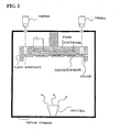
- FIG. 1 is an illustration showing a mask vapor deposition system according to a first embodiment of the present invention.
- Mask vapor deposition is performed in a vacuum.
- a necessary mechanism such as a transfer mechanism, which is not shown in FIG. 1, is placed in a vacuum chamber 50, wherein the mechanism is used for transferring a glass substrate 20 (that is a subject to be attracted, this embodiment uses the glass substrate 20 as an example, and the present invention is not limited thereto), which is a subject for deposition.
- An electrostatic chuck stage (hereinafter simply referred to as a stage) 1 is a flat table for attracting the glass substrate 20 by electrostatic chucking, correcting the warp, and preventing a deposition mask 2 that has been aligned from being misaligned thereafter.
- the electrostatic chucking is as follows: surfaces of the glass substrate 20 and stage 1 are positively or negatively charged by applying voltages to metal electrodes (hereinafter referred to as electrodes) 1A placed in the stage 1, and the glass substrate 20 is attracted and retained (hereinafter referred to as attractive retainment) by the Janssen-Rahbek force (also referred to as the Jhonsen-Rahbek force).
- the electrodes 1A placed in the stage 1 are arranged in such a manner that the electrodes 1A adjacent to each other have different polarities, and this arrangement is referred to as a bipolar type.
- the deposition subject In this type, the deposition subject must be grounded, and therefore the glass substrate 20 that is the deposition subject must be wired.
- the bipolar type is employed in order to avoid wiring the glass substrate 20.
- the stage 1 is turned with a turning mechanism (not shown). In order to align the deposition mask 2 with the glass substrate 20, the stage 1 can be transferred by the operation of a stepping motor (not shown).
- the deposition mask 2 must be as flat as possible. A tension is preferably applied to the entire deposition mask 2 with a holder 30 for transferring the deposition mask 2. However, openings of a mask pattern must be prevented from being deformed. It is preferable to prepare the deposition mask 2 using a semiconductor substrate containing silicon or the like because such a substrate is superior in flatness.
- the deposition mask 2 may be prepared using metal such as a nickel alloy.
- the deposition mask 2 has alignment marks, not shown in FIG. 1, used for the alignment with the glass substrate 20.
- the glass substrate 20 also has such alignment marks. In this embodiment, each of them has the two alignment marks in accordance with the number of cameras; however, the number of the marks is not limited to the above.
- Cameras 3A and 3B include, for example, CCD cameras and are used for aligning the deposition mask 2 with the glass substrate 20.
- part of the vacuum chamber 50 are transparent and perforations extend through parts of the stage 1, thereby taking pictures of parts of the glass substrate 20 through the perforations. Obtained images are displayed on a display means (not shown) placed out of the vacuum chamber 50.
- An operating person (operator) inputs data into an indicating unit (not shown) based on each image having the alignment marks placed on the glass substrate 20 and deposition mask 2, for alignment and then moves the stage 1 to perform alignment. Since the glass substrate 20 is transparent, the alignment marks placed on the deposition mask 2 can be displayed as an image.
- the alignment is manually performed; however, the alignment may be automatically performed in such a manner that, for example, a processing means such as a computer or the like processes the obtained image to control the transfer of the stage 1. Furthermore, two pairs of marks are aligned using the two cameras 3A and 3B; however, the present invention is not limited to such a manner.
- Reference numeral 61 represents a crucible functioning as an evaporation source that evaporates a deposition material to be deposited on the glass substrate 20 by heating.
- the single crucible 61 is placed at the center area of the vacuum chamber 50; however, the present invention is not limited to such a configuration.
- Crucibles may be arranged at a plurality of areas and various configurations may be employed.
- a deposition procedure according to this vapor deposition method is described below.
- the glass substrate 20 is transferred to the stage 1 with the transfer mechanism. In this operation, the glass substrate 20 is transferred to such a position that the cameras 3A and 3B can take pictures of the alignment marks placed on the glass substrate 20.
- the electrodes 1A are then charged, whereby the glass substrate 20 is attractively retained to the stage 1 by the electrostatic chucking. In this attracting operation, the warp of the glass substrate 20 is corrected, whereby a gap between the glass substrate 20 and stage is eliminated.
- the deposition mask 2 is brought as close as possible to the glass substrate 20 as long as the deposition mask 2 is not in contact with the glass substrate 20. In this embodiment, they are brought close to each other until the distance therebetween reaches, for example, 20 ⁇ m.
- the operator inputs data into the indicating unit, as described above, while the above situation is maintained, and then transfers the stage 1 to perform alignment. After the alignment is performed, the deposition mask 2 is further brought 20 ⁇ m close to the glass substrate 20, whereby the deposition mask 2 is allowed to come into close contact with the glass substrate 20. In this operation, the warp of the glass substrate 20 is corrected by the electrostatic chucking, thereby enhancing the adhesion to the deposition mask 2.
- the alignment can be precisely performed without generating shock.
- the warp of the glass substrate 20 is corrected with the stage 1, the adhesion between the glass substrate 20 and deposition mask 2 is lowered due to radiant heat or the like if the deposition mask 2 is made of metal or the like.
- a magnet may be placed on the side of the stage 1, whereby the deposition mask 2 is brought into close contact with the glass substrate 20 by magnetic force.
- a permanent magnet may be used, but an electromagnet is preferably used because the magnetic force can be controlled. Since the magnet is used for securely bringing the deposition mask 2 into close contact with the glass substrate 20 after the electrostatic chucking, shock is not generated after the alignment, in contrast to known methods.
- the crucible 61 is heated, whereby the deposition material is vaporized and then vacuum-deposited on unmasked regions of the glass substrate.
- the stage 1 is turned with the turning mechanism, whereby the deposition material is uniformly deposited over the regions of the glass substrate 20 for deposition.
- the alignment is further performed and the deposition is repeated if other regions are subjected to the deposition.
- the deposition mask 2 is released from the glass substrate 20, the attractive retainment by the electrostatic chucking is ceased, and the glass substrate 20 is transferred from the stage 1 with the transfer mechanism.
- the glass substrate 20 is attractively retained on the stage 1 by the electrostatic chucking in advance, the warp of the glass substrate 20 is corrected, and the deposition material is deposited on the glass substrate 20 in such a manner that the deposition mask 2 is brought into close contact with the glass substrate 20. Therefore, the adhesion between the deposition mask 2 and the glass substrate 20, which is a subject for deposition, can be enhanced. Thus, the deposition material is prevented from sticking onto shadow areas, whereby the deposition can be precisely performed. Since the electrostatic chucking is employed, the deposition mask 2 can be prepared using a material that is not attracted by a magnet. Thus, a material, such as silicon, which has high processing accuracy and is hardly deformed, can be used.
- the center area is not deformed by the attraction, whereby the alignment can be performed in a short time.
- the attraction is not performed after the deposition subject is brought into close contact with the mask. Therefore, displacement is not caused by shock generated during the attraction, whereby the deposition can be performed while the precise alignment is maintained.
- FIG. 2 is a schematic view showing an deposition mask 2A according to a second embodiment of the present invention.
- the deposition mask 2A of this embodiment includes mask pattern portions 11 each comprising a silicon substrate and having high definition.
- the mask pattern portions 11 each function as an electrode and therefore the deposition mask has an electrostatic chucking function.
- the mask pattern portions 11 are each bonded to corresponding perforated regions of a mask holder 10 made of, for example, glass.
- the nine mask pattern portions 11 can be bonded to the mask holder 10 shown in FIG. 2.
- the mask holder 10 has printed wires 12 for supplying charges from a power source to the mask pattern portions 11 each functioning as an electrode.
- the bipolar type is employed.
- the printed wires 12 are arranged such that the mask pattern portions 11 adjacent to each other have different polarities.
- FIG. 3 is a sectional view taken along with the line I-I of the deposition mask 2A in FIG. 2.
- a surface to be brought into contact with a subject for deposition is covered with an insulating layer 14 of, for example, silicon dioxide (hereinafter referred to as SiO 2 ) obtained by thermal oxidation. Therefore, a current is not directly applied to the deposition subject.
- SiO 2 silicon dioxide
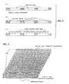
- FIG. 4 is an illustration showing a process for preparing a mask pattern portion 11.
- a procedure of manufacturing the mask pattern portion 11 is described with reference to FIG. 4.
- Both faces of a silicon substrate 13 are planarized by polishing.
- the thickness of the silicon substrate 13 is not particularly limited; however, the silicon substrate 13 must have a thickness that is sufficient to endure attraction and sufficient to obtain high adhesion.
- the silicon substrate 13 is placed in a thermal oxidation furnace.
- the silicon substrate 13 is thermally oxidized at a predetermined temperature for a predetermined time in an atmosphere containing oxygen and steam.
- the SiO 2 insulating layer 14 having a thickness of about 1 ⁇ m is formed on a surface of the silicon substrate 13 (FIG. 4(a)).
- the insulating layer 14 is formed by a thermal oxidation method; however, the insulating layer 14A may be formed by a CVD (Chemical vapor deposition) method or the like.
- SiO 2 of the mask to be manufactured is patterned using a photomask by a photolithographic method. Thereby, a resist portion for SiO 2 is formed. That is, regions on which the resist portion is not disposed finally form openings.
- the insulating layer 14 is then etched with an etching solution containing fluoric acid (FIG. 4(b)). Thereby, SiO 2 remains at the resist portion.
- the silicon substrate 13 is soaked in an alkaline solution such as an aqueous potassium hydroxide (KOH) solution, thereby wet-etching unpatterned areas in the (111) crystal face in an anisotropic manner for a crystal.
- KOH aqueous potassium hydroxide
- openings 15 and tapered perforations 16 having a (111) crystal plane are formed (FIG. 4(c)).
- the etching proceeds at an angle of about 54.7°.
- the openings 15 on a wider side are made to face an evaporation source (downward) and the opening on a narrower side where the perforations 16 are formed, are made to face the deposition subject. Therefore, even if the evaporation source is only placed at the center, peripheral areas of the deposition subject are not covered with the mask pattern portions 11 and are subjected to deposition because the openings 15 are expanded downwards.
- FIG. 5 is an illustration showing a process for preparing the mask holder 10.
- a procedure of preparing the mask holder 10 is described with reference to FIG. 5.
- Perforations 18 are formed in a holder glass substrate 17, which is a material for preparing the mask holder 10, in advance (FIG. 5(a)).
- a method for forming the perforations 18 includes, for example, a cutting method using a laser, a microblast machining method, and the like.
- the microblast is a machining technique of performing physical etching by applying abrasive grains.
- a thin-film of Au/Cr (chromium-gold alloy) is formed on a face, to which the mask pattern portions 11 are to be bonded, by a sputtering method. Patterning is then performed by a photolithographic method, thereby allowing resist portions to remain on regions for forming the printed wires 12. Other regions having no resist portion are removed by an etching method, and the resist portions are then removed, thereby forming the printed wires 12 (FIG. 5(b)).
- the prepared mask pattern portions 11 are stuck on the face (FIG. 5(c)).
- an adhesive is used for the sticking.
- the adhesive contains conductive particles so as to connect the mask pattern portions 11 to the printed wires 12 electrically.
- the mask pattern portions 11 are pressed against the mask holder 10 and a pressure is applied thereto, thereby obtaining the deposition mask 2A.
- the deposition mask since the deposition mask has an electrostatic chucking function, the adhesion between the deposition mask and the deposition subject can be enhanced. Furthermore, since a shock is not applied to the deposition mask and the deposition subject that have been aligned with each other in the preparing steps, vapor deposition can be performed while precise alignment is maintained.
- FIG. 6 is an illustration showing an deposition mask 2B according to a third embodiment of the present invention.
- the mask pattern portions 11 are stuck on the mask holder 10, thereby preparing a deposition mask.
- a deposition mask is prepared using a single silicon wafer. For example, when a 12-inch wafer is used, a deposition mask with a side having a length of about 20 cm can be prepared.
- Au/Cr chromium-gold alloy
- wiring lines 19A functions as a positive electrode
- the wiring line 19B functions as a negative electrode when charges are supplied from a power source.
- wiring is performed so as to form an interdigital structure, thereby reducing the distance between the positive electrode and negative electrode.
- the electrostatic attraction is increased and the Janssen-Rahbek force (attracting force) is increased.
- FIG. 7 is an illustration showing a process for preparing the deposition mask 2B.
- the process for preparing the deposition mask according to this embodiment is described below. Both faces of a silicon substrate 13A are planarized by polishing and the resulting silicon substrate 13A is placed in a thermal oxidation furnace in the same manner as that of preparing the mask pattern portions 11 in the above-mentioned second embodiment.
- the silicon substrate 13A is thermally oxidized at a predetermined temperature for a predetermined time in an atmosphere containing oxygen and steam, thereby forming an insulating layer 14A of SiO 2 (FIG. 7(a)).
- the thermal oxidation is performed; however, the insulating layer 14A may be formed by a CVD method or the like.
- a thin-film is formed by a sputtering method using Au/Cr (chromium-gold alloy). Patterning is performed by a photolithographic method so as to form an interdigital pattern, thereby providing resist portions on regions for forming wiring lines. Other regions having no resist portion are removed by an etching method, and the resist portions are then removed, thereby forming wiring lines 19A 19B of Au/Cr (FIG. 7(b)).
- the distance between the wiring lines is not limited to that shown in FIG. 7(b), and the wiring line 19A functioning as a positive electrode and the wiring line 19B functioning as a negative electrode are alternately arranged.
- the wiring lines have a height of about 2000-3000 angstroms (2 to 3 ⁇ 10 -7 m). In order to increase the attracting force, the interdigital arrangement is preferable; however, the arrangement of the wiring lines is not limited to the interdigital arrangement.
- SiO 2 of the mask to be manufactured is patterned using a photomask by a photolithographic method, thereby forming resist portions for SiO 2 .
- the insulating layer 14A is then etched with an etching solution containing fluoric acid (FIG. 7(c)). Thereby, SiO 2 remains at the resist portions.
- the silicon substrate 13A is soaked in an alkaline solution such as an aqueous potassium hydroxide (KOH) solution, thereby wet-etching unpatterned areas in the (111) crystal face in an anisotropic manner for a crystal (FIG. 7(d)).
- KOH aqueous potassium hydroxide
- an insulating layer 14B of SiO 2 is formed by a CVD method or the like in order to protect the interdigital wiring lines and insulate the wiring lines from a subject for deposition(FIG. 7(e)). Since the wiring lines of Au/Cr are arranged, a surface of the deposition mask 2B has irregularities in some cases. Since the wiring lines have a height of about 2000-3000 angstroms (2 to 3 ⁇ 10 -7 m), the irregularities have such an order of magnitude. This order of magnitude is negligible as compared with the flatness of an deposition mask surface that is necessary in manufacturing organic EL panels.
- the SiO 2 layer is polished by a CMP (Chemical-Mechanical Polishing) method or the like, thereby planarizing the surface of the deposition mask 2B. Only SiO 2 on the back face is then removed (FIG. 7(f)).
- CMP Chemical-Mechanical Polishing
- the deposition mask 2B is prepared using a single silicon substrate, the deposition mask having high flatness and high definition can be prepared. Since the wiring lines are placed on the silicon substrate and arranged in an interdigital pattern, and the positive and negative electrodes are alternately arranged, the electrostatic attraction is increased, thereby increasing the attracting force.
- the deposition mask having the Au/Cr wiring lines arranged in an interdigital pattern is prepared. This can be applied to the mask pattern portions 11 of the second embodiment. In this case, as the mask pattern portions 11 each have a positive electrode and negative electrode, the wiring pattern of the mask becomes different from that of the printed wires 12 shown in FIG. 2.
- the prepared masks are used for vapor deposition.
- the present invention is not limited such a use and the masks may be used for processing such as sputtering or etching.
- a process for manufacturing a mask is not limited to the processes shown above and may include chemical or physical processing processes such as an etching process and sputtering process.
- a dry etching process such as reactive ion-etching process in addition to the wet-etching process and sputtering process.
- FIG. 8 is an illustration showing parts of a process for manufacturing a display panel including EL elements according to a sixth embodiment.
- a process for manufacturing a color active matrix display panel including organic EL elements is described.
- the following light-emitting substances are used as deposition materials: three light-emitting substances of corresponding organic compounds for emitting light rays of corresponding colors, for example, additive primary colors: R (red), G (green), and B (blue).
- the three light-emitting substances are deposited on a rectangular glass substrate 20 in such a manner that triplets of the light-emitting substances for each emitting corresponding R, G, and B light rays are repeatedly arranged in parallel to a side (usually a shorter side) of the glass substrate 20 at regular intervals.
- the arranged light-emitting substances must correspond to respective elements, which are TFTs disposed on the glass substrate 20.
- a deposition mask 2C of this embodiment has a mask pattern corresponding to the above deposition. For example, openings are placed at the corresponding interval between the triplets (that is, for every triplet of three pixels) depending on the number of the triplets. The openings have a tapered shape, as described in the second embodiment.
- three alignment marks for the triplets are arranged in such a manner that the marks are displaced for each pixel. Three types of deposition masks are prepared, and vapor deposition may be performed while the deposition masks are changed. Before the glass substrate 20 is subjected to the steps shown in FIG.
- the glass substrate 20 is subjected to a step of forming a transistor, a capacitor, wiring lines, a driving circuit, and the like for every pixel on the glass substrate 20 and a step of forming a transparent electrode for every pixel and then forming TFTs. Furthermore, the glass substrate 20 is subjected to a step of forming (layering) hole transport/injection layers on the transparent electrodes according to needs.
- the glass substrate 20 is transferred into a vacuum chamber 50 and then attractively retained on a stage 1 or a deposition mask 2A by electrostatic chucking in the same manner as that of the first embodiment.
- the deposition mask 2A and the glass substrate 20 are aligned at a position for depositing the R light-emitting substance and then brought into close contact with each other.
- the glass substrate 20 is brought into close contact with the deposition mask 2C and then electrostatically chucked by the mask so as to be attractively retained on the deposition mask 2C.
- the R light-emitting substance is deposited, thereby forming light-emitting layers functioning as cores of EL elements (FIG. 8(a)).
- the R light-emitting substance includes, for example, BSB-BCN.
- the deposition mask 2C and the glass substrate 20 are aligned at a position (a position displaced for one pixel) for depositing the G light-emitting substance and then brought into close contact with each other.
- the G light-emitting substance is deposited, thereby forming light-emitting layers (FIG. 8(b)).
- the deposition mask 2C and the glass substrate 20 are aligned at a position for depositing the B light-emitting substance with the position displaced further for one pixel and then brought into close contact with each other.
- the B light-emitting substance is deposited, thereby forming light-emitting layers (FIG. 8(c)).
- a step of forming cathode layers such as electron transport/injection layers or the like is performed according to needs, thereby manufacturing the active matrix display panel.
- the hole transport/injection layers, light-emitting layers, and electron transport/injection layers are separately formed.
- the deposition mask 2C is brought into close contact with the glass substrate 20 and the hole transport/injection layers, light-emitting layers, and electron transport layers may be then formed by deposition.
- the following procedure may be performed: the electron transport layers are formed in advance and the light-emitting layers and hole transport/injection layers are then formed.
- FIGS. 9A-9C is an illustration showing electronic devices according to a seventh embodiment of the present invention.
- FIG. 9A shows a PDA (Personal Digital Assistant)
- FIG. 9B shows a mobile phone
- FIG. 9C shows a digital camera.
- a display panel of the present invention can be used for such electronic devices, such as computers and game machines, having a display function and including a display panel, the devices being not shown in this embodiment.
Landscapes
- Chemical & Material Sciences (AREA)
- Mechanical Engineering (AREA)
- Chemical Kinetics & Catalysis (AREA)
- Engineering & Computer Science (AREA)
- Materials Engineering (AREA)
- Metallurgy (AREA)
- Organic Chemistry (AREA)
- Physics & Mathematics (AREA)
- Nonlinear Science (AREA)
- General Physics & Mathematics (AREA)
- Optics & Photonics (AREA)
- Crystallography & Structural Chemistry (AREA)
- Physical Vapour Deposition (AREA)
- Electroluminescent Light Sources (AREA)
Applications Claiming Priority (2)
| Application Number | Priority Date | Filing Date | Title |
|---|---|---|---|
| JP2002350950A JP2004183044A (ja) | 2002-12-03 | 2002-12-03 | マスク蒸着方法及び装置、マスク及びマスクの製造方法、表示パネル製造装置、表示パネル並びに電子機器 |
| JP2002350950 | 2002-12-03 |
Publications (2)
| Publication Number | Publication Date |
|---|---|
| EP1426462A2 true EP1426462A2 (fr) | 2004-06-09 |
| EP1426462A3 EP1426462A3 (fr) | 2004-08-04 |
Family
ID=32310692
Family Applications (1)
| Application Number | Title | Priority Date | Filing Date |
|---|---|---|---|
| EP03027352A Withdrawn EP1426462A3 (fr) | 2002-12-03 | 2003-11-27 | Procédé et appareillage de déposition en phase vapeur utilisant un masque, masque, procédé de fabrication d'un panneau d'affichage, panneau d'affichage et appareil électronique |
Country Status (6)
| Country | Link |
|---|---|
| US (1) | US20040142108A1 (fr) |
| EP (1) | EP1426462A3 (fr) |
| JP (1) | JP2004183044A (fr) |
| KR (1) | KR100641478B1 (fr) |
| CN (1) | CN1522098A (fr) |
| TW (1) | TWI235184B (fr) |
Cited By (5)
| Publication number | Priority date | Publication date | Assignee | Title |
|---|---|---|---|---|
| EP1584703A1 (fr) * | 2004-03-23 | 2005-10-12 | Seiko Epson Corporation | Masque, procédé pour sa fabrication, procédé de fabrication d'un motif en couche mince, procédé de fabrication d'un objet electro-optique et équipement électronique |
| WO2017205479A1 (fr) | 2016-05-24 | 2017-11-30 | Emagin Corporation | Système de dépôt par masque perforé et procédé associé |
| EP3133183A4 (fr) * | 2014-04-18 | 2017-12-06 | Boe Technology Group Co. Ltd. | Dispositif magnétique, dispositif d'évaporation et procédé d'évaporation |
| US10581025B2 (en) | 2016-03-03 | 2020-03-03 | Lg Display Co., Ltd. | Deposition apparatus for organic light-emitting diodes |
| US11275315B2 (en) | 2016-05-24 | 2022-03-15 | Emagin Corporation | High-precision shadow-mask-deposition system and method therefor |
Families Citing this family (150)
| Publication number | Priority date | Publication date | Assignee | Title |
|---|---|---|---|---|
| KR101303447B1 (ko) * | 2009-01-21 | 2013-09-05 | 엘지디스플레이 주식회사 | 유기전계발광표시장치의 증착장치 |
| JP4651918B2 (ja) * | 2003-05-21 | 2011-03-16 | 東北パイオニア株式会社 | 有機elパネルの製造方法 |
| JP2005163099A (ja) * | 2003-12-02 | 2005-06-23 | Seiko Epson Corp | マスク、マスクの製造方法、有機el装置の製造方法、有機el装置 |
| JP4510609B2 (ja) * | 2004-12-21 | 2010-07-28 | 株式会社アルバック | 基板とマスクのアライメント方法および有機薄膜蒸着方法ならびにアライメント装置 |
| JP4375232B2 (ja) * | 2005-01-06 | 2009-12-02 | セイコーエプソン株式会社 | マスク成膜方法 |
| US20060159893A1 (en) * | 2005-01-19 | 2006-07-20 | Visteon Global Technologies, Inc. | Decorative articles for automotive glazing and methods of making same |
| US20080003416A1 (en) * | 2005-01-19 | 2008-01-03 | Watson Rodney B | Decorative Articles for Automotive Glazing and Methods of Making the Same |
| JP4609756B2 (ja) * | 2005-02-23 | 2011-01-12 | 三井造船株式会社 | 成膜装置のマスク位置合わせ機構および成膜装置 |
| JP4609754B2 (ja) * | 2005-02-23 | 2011-01-12 | 三井造船株式会社 | マスククランプの移動機構および成膜装置 |
| JP4609755B2 (ja) * | 2005-02-23 | 2011-01-12 | 三井造船株式会社 | マスク保持機構および成膜装置 |
| JP4609757B2 (ja) * | 2005-02-23 | 2011-01-12 | 三井造船株式会社 | 成膜装置における基板装着方法 |
| JP4624824B2 (ja) * | 2005-03-04 | 2011-02-02 | 京セラ株式会社 | メタルマスクの製造方法およびメタルマスク |
| JP4609759B2 (ja) * | 2005-03-24 | 2011-01-12 | 三井造船株式会社 | 成膜装置 |
| KR101146978B1 (ko) * | 2005-05-14 | 2012-05-23 | 삼성모바일디스플레이주식회사 | 유기전계 발광소자용 기판 및 이를 이용한 유기전계발광소자의 제조방법 |
| JP4428285B2 (ja) | 2005-05-16 | 2010-03-10 | セイコーエプソン株式会社 | マスク保持構造、成膜方法、及び電気光学装置の製造方法 |
| US20060274474A1 (en) * | 2005-06-01 | 2006-12-07 | Lee Chung J | Substrate Holder |
| KR101289345B1 (ko) * | 2005-07-19 | 2013-07-29 | 주성엔지니어링(주) | 섀도우 마스크와 이를 이용한 정렬장치 |
| KR100762046B1 (ko) * | 2006-01-25 | 2007-09-28 | 엘에스전선 주식회사 | 회전 마스크를 구비한 대면적 박막 증착 장치 |
| US20070262326A1 (en) * | 2006-05-10 | 2007-11-15 | Touchtek Corporation | LED multi-layer metals primary electrodes manufacturing process & installation |
| KR100712953B1 (ko) * | 2006-06-16 | 2007-05-02 | 두산디앤디 주식회사 | 기판 얼라인장치 및 이를 이용한 기판얼라인방법 |
| KR100787457B1 (ko) * | 2006-08-31 | 2007-12-26 | 삼성에스디아이 주식회사 | 기판 정렬 장치 및 이를 포함하는 유기 발광 표시 장치용제조 장치 |
| DE102007027435A1 (de) * | 2007-06-14 | 2008-12-18 | X-Fab Semiconductor Foundries Ag | Verfahren und Vorrichtung zur strukturierten Schichtabscheidung auf prozessierten Mikrosystemtechnikwafern |
| JP5262226B2 (ja) * | 2007-08-24 | 2013-08-14 | 大日本印刷株式会社 | 蒸着マスクおよび蒸着マスクの製造方法 |
| WO2009069743A1 (fr) * | 2007-11-30 | 2009-06-04 | Canon Anelva Corporation | Appareil de traitement de substrat et procédé de traitement de substrat |
| WO2009084623A1 (fr) * | 2007-12-27 | 2009-07-09 | Canon Anelva Corporation | Appareil de traitement, élément d'émission d'électrons et procédé de fabrication d'un dispositif d'affichage électroluminescent organique |
| KR101001454B1 (ko) * | 2009-01-23 | 2010-12-14 | 삼성모바일디스플레이주식회사 | 정전척 및 이를 구비한 유기전계발광 소자의 제조장치 |
| JP5620146B2 (ja) | 2009-05-22 | 2014-11-05 | 三星ディスプレイ株式會社Samsung Display Co.,Ltd. | 薄膜蒸着装置 |
| TWI475124B (zh) * | 2009-05-22 | 2015-03-01 | Samsung Display Co Ltd | 薄膜沉積設備 |
| US8882920B2 (en) * | 2009-06-05 | 2014-11-11 | Samsung Display Co., Ltd. | Thin film deposition apparatus |
| US8882921B2 (en) * | 2009-06-08 | 2014-11-11 | Samsung Display Co., Ltd. | Thin film deposition apparatus |
| US8802200B2 (en) | 2009-06-09 | 2014-08-12 | Samsung Display Co., Ltd. | Method and apparatus for cleaning organic deposition materials |
| US9174250B2 (en) | 2009-06-09 | 2015-11-03 | Samsung Display Co., Ltd. | Method and apparatus for cleaning organic deposition materials |
| KR101074792B1 (ko) * | 2009-06-12 | 2011-10-19 | 삼성모바일디스플레이주식회사 | 박막 증착 장치 |
| KR101097311B1 (ko) * | 2009-06-24 | 2011-12-21 | 삼성모바일디스플레이주식회사 | 유기 발광 디스플레이 장치 및 이를 제조하기 위한 유기막 증착 장치 |
| KR101117719B1 (ko) * | 2009-06-24 | 2012-03-08 | 삼성모바일디스플레이주식회사 | 박막 증착 장치 |
| KR101117720B1 (ko) * | 2009-06-25 | 2012-03-08 | 삼성모바일디스플레이주식회사 | 박막 증착 장치 및 이를 이용한 유기 발광 소자 제조 방법 |
| KR20110014442A (ko) * | 2009-08-05 | 2011-02-11 | 삼성모바일디스플레이주식회사 | 박막 증착 장치 및 이를 이용한 유기 발광 디스플레이 장치의 제조 방법 |
| US20110033621A1 (en) * | 2009-08-10 | 2011-02-10 | Samsung Mobile Display Co., Ltd. | Thin film deposition apparatus including deposition blade |
| KR101127575B1 (ko) * | 2009-08-10 | 2012-03-23 | 삼성모바일디스플레이주식회사 | 증착 가림막을 가지는 박막 증착 장치 |
| JP5676175B2 (ja) * | 2009-08-24 | 2015-02-25 | 三星ディスプレイ株式會社Samsung Display Co.,Ltd. | 薄膜蒸着装置及びこれを利用した有機発光表示装置の製造方法 |
| KR101127578B1 (ko) * | 2009-08-24 | 2012-03-23 | 삼성모바일디스플레이주식회사 | 박막 증착 장치, 이를 이용한 유기 발광 디스플레이 장치의 제조방법 및 이에 따라 제조된 유기 발광 디스플레이 장치 |
| US8486737B2 (en) * | 2009-08-25 | 2013-07-16 | Samsung Display Co., Ltd. | Thin film deposition apparatus and method of manufacturing organic light-emitting display device by using the same |
| JP5328726B2 (ja) | 2009-08-25 | 2013-10-30 | 三星ディスプレイ株式會社 | 薄膜蒸着装置及びこれを利用した有機発光ディスプレイ装置の製造方法 |
| JP5677785B2 (ja) * | 2009-08-27 | 2015-02-25 | 三星ディスプレイ株式會社Samsung Display Co.,Ltd. | 薄膜蒸着装置及びこれを利用した有機発光表示装置の製造方法 |
| JP5611718B2 (ja) * | 2009-08-27 | 2014-10-22 | 三星ディスプレイ株式會社Samsung Display Co.,Ltd. | 薄膜蒸着装置及びこれを利用した有機発光表示装置の製造方法 |
| US8696815B2 (en) | 2009-09-01 | 2014-04-15 | Samsung Display Co., Ltd. | Thin film deposition apparatus |
| US20110052795A1 (en) * | 2009-09-01 | 2011-03-03 | Samsung Mobile Display Co., Ltd. | Thin film deposition apparatus and method of manufacturing organic light-emitting display device by using the same |
| JP2011074423A (ja) * | 2009-09-29 | 2011-04-14 | Hitachi High-Technologies Corp | 有機elデバイス製造装置及び有機elデバイス製造方法並びに成膜装置及び成膜方法 |
| US8876975B2 (en) * | 2009-10-19 | 2014-11-04 | Samsung Display Co., Ltd. | Thin film deposition apparatus |
| KR101146982B1 (ko) | 2009-11-20 | 2012-05-22 | 삼성모바일디스플레이주식회사 | 박막 증착 장치 및 유기 발광 디스플레이 장치 제조 방법 |
| KR101084184B1 (ko) * | 2010-01-11 | 2011-11-17 | 삼성모바일디스플레이주식회사 | 박막 증착 장치 |
| KR101174875B1 (ko) * | 2010-01-14 | 2012-08-17 | 삼성디스플레이 주식회사 | 박막 증착 장치, 이를 이용한 유기 발광 디스플레이 장치의 제조방법 및 이에 따라 제조된 유기 발광 디스플레이 장치 |
| CN101777295B (zh) * | 2010-01-29 | 2012-07-18 | 信利半导体有限公司 | Oled显示器的检测线布线方法及制造方法 |
| CN101789208B (zh) * | 2010-01-29 | 2012-10-03 | 信利半导体有限公司 | Oled显示器的检测线布线方法及制造方法 |
| KR101193186B1 (ko) * | 2010-02-01 | 2012-10-19 | 삼성디스플레이 주식회사 | 박막 증착 장치, 이를 이용한 유기 발광 디스플레이 장치의 제조방법 및 이에 따라 제조된 유기 발광 디스플레이 장치 |
| KR101156441B1 (ko) | 2010-03-11 | 2012-06-18 | 삼성모바일디스플레이주식회사 | 박막 증착 장치 |
| JP2011195907A (ja) * | 2010-03-19 | 2011-10-06 | Tokyo Electron Ltd | マスク保持装置及び薄膜形成装置 |
| JP5525894B2 (ja) * | 2010-03-31 | 2014-06-18 | 富士フイルム株式会社 | 固体撮像素子の製造方法 |
| KR101202348B1 (ko) | 2010-04-06 | 2012-11-16 | 삼성디스플레이 주식회사 | 박막 증착 장치 및 이를 이용한 유기 발광 표시 장치의 제조 방법 |
| US9055653B2 (en) | 2010-04-12 | 2015-06-09 | Sharp Kabushiki Kaisha | Deposition apparatus and deposition method |
| US8894458B2 (en) | 2010-04-28 | 2014-11-25 | Samsung Display Co., Ltd. | Thin film deposition apparatus, method of manufacturing organic light-emitting display device by using the apparatus, and organic light-emitting display device manufactured by using the method |
| KR101223723B1 (ko) | 2010-07-07 | 2013-01-18 | 삼성디스플레이 주식회사 | 박막 증착 장치, 이를 이용한 유기 발광 디스플레이 장치의 제조방법 및 이에 따라 제조된 유기 발광 디스플레이 장치 |
| KR101673017B1 (ko) | 2010-07-30 | 2016-11-07 | 삼성디스플레이 주식회사 | 박막 증착 장치 및 이를 이용한 유기 발광 표시장치의 제조 방법 |
| KR101678056B1 (ko) | 2010-09-16 | 2016-11-22 | 삼성디스플레이 주식회사 | 박막 증착 장치, 이를 이용한 유기 발광 디스플레이 장치의 제조방법 및 이에 따라 제조된 유기 발광 디스플레이 장치 |
| KR20120029166A (ko) | 2010-09-16 | 2012-03-26 | 삼성모바일디스플레이주식회사 | 박막 증착 장치, 이를 이용한 유기 발광 디스플레이 장치의 제조방법 및 이에 따라 제조된 유기 발광 디스플레이 장치 |
| KR101723506B1 (ko) | 2010-10-22 | 2017-04-19 | 삼성디스플레이 주식회사 | 유기층 증착 장치 및 이를 이용한 유기 발광 디스플레이 장치의 제조 방법 |
| KR101738531B1 (ko) | 2010-10-22 | 2017-05-23 | 삼성디스플레이 주식회사 | 유기 발광 디스플레이 장치의 제조 방법 및 이에 따라 제조된 유기 발광 디스플레이 장치 |
| KR20120045865A (ko) | 2010-11-01 | 2012-05-09 | 삼성모바일디스플레이주식회사 | 유기층 증착 장치 |
| KR20120065789A (ko) | 2010-12-13 | 2012-06-21 | 삼성모바일디스플레이주식회사 | 유기층 증착 장치 |
| KR101760897B1 (ko) | 2011-01-12 | 2017-07-25 | 삼성디스플레이 주식회사 | 증착원 및 이를 구비하는 유기막 증착 장치 |
| JP5773731B2 (ja) * | 2011-05-02 | 2015-09-02 | 株式会社アルバック | 真空処理装置 |
| KR101923174B1 (ko) | 2011-05-11 | 2018-11-29 | 삼성디스플레이 주식회사 | 정전 척, 상기 정전 척을 포함하는 박막 증착 장치 및 이를 이용한 유기 발광 표시 장치의 제조 방법 |
| KR101840654B1 (ko) | 2011-05-25 | 2018-03-22 | 삼성디스플레이 주식회사 | 유기층 증착 장치 및 이를 이용한 유기 발광 디스플레이 장치의 제조 방법 |
| KR101852517B1 (ko) | 2011-05-25 | 2018-04-27 | 삼성디스플레이 주식회사 | 유기층 증착 장치 및 이를 이용한 유기 발광 디스플레이 장치의 제조 방법 |
| KR101857992B1 (ko) | 2011-05-25 | 2018-05-16 | 삼성디스플레이 주식회사 | 패터닝 슬릿 시트 어셈블리, 유기막 증착 장치, 유기 발광 표시 장치 제조 방법 및 유기 발광 표시 장치 |
| KR101857249B1 (ko) | 2011-05-27 | 2018-05-14 | 삼성디스플레이 주식회사 | 패터닝 슬릿 시트 어셈블리, 유기막 증착 장치, 유기 발광 표시장치제조 방법 및 유기 발광 표시 장치 |
| KR101826068B1 (ko) | 2011-07-04 | 2018-02-07 | 삼성디스플레이 주식회사 | 유기층 증착 장치 |
| KR20130004830A (ko) | 2011-07-04 | 2013-01-14 | 삼성디스플레이 주식회사 | 유기층 증착 장치 및 이를 이용한 유기 발광 표시 장치의 제조 방법 |
| KR20130010730A (ko) | 2011-07-19 | 2013-01-29 | 삼성디스플레이 주식회사 | 증착 소스 및 이를 구비한 증착 장치 |
| TWI475736B (zh) * | 2011-07-26 | 2015-03-01 | Innolux Corp | 電激發光顯示裝置的製作方法以及鍍膜機台 |
| KR20130015144A (ko) | 2011-08-02 | 2013-02-13 | 삼성디스플레이 주식회사 | 증착원어셈블리, 유기층증착장치 및 이를 이용한 유기발광표시장치의 제조 방법 |
| KR20130057794A (ko) * | 2011-11-24 | 2013-06-03 | 삼성디스플레이 주식회사 | 증착용 마스크 및 증착용 마스크의 제조 방법 |
| KR20130069037A (ko) | 2011-12-16 | 2013-06-26 | 삼성디스플레이 주식회사 | 유기층 증착 장치, 이를 이용한 유기 발광 표시 장치의 제조 방법 및 유기 발광 표시 장치 |
| CN103205687B (zh) * | 2012-01-16 | 2016-03-02 | 昆山允升吉光电科技有限公司 | 蒸镀掩模板及其制作方法 |
| KR102015872B1 (ko) | 2012-06-22 | 2019-10-22 | 삼성디스플레이 주식회사 | 유기층 증착 장치, 이를 이용한 유기 발광 디스플레이 장치의 제조 방법 및 이에 따라 제조된 유기 발광 디스플레이 장치 |
| KR101959974B1 (ko) | 2012-07-10 | 2019-07-16 | 삼성디스플레이 주식회사 | 유기층 증착 장치, 이를 이용한 유기 발광 디스플레이 장치의 제조 방법 및 이에 따라 제조된 유기 발광 디스플레이 장치 |
| KR102013315B1 (ko) | 2012-07-10 | 2019-08-23 | 삼성디스플레이 주식회사 | 유기 발광 디스플레이 장치의 제조 방법 및 이에 따라 제조된 유기 발광 디스플레이 장치 |
| CN103545460B (zh) | 2012-07-10 | 2017-04-12 | 三星显示有限公司 | 有机发光显示装置、有机发光显示设备及其制造方法 |
| US9461277B2 (en) | 2012-07-10 | 2016-10-04 | Samsung Display Co., Ltd. | Organic light emitting display apparatus |
| KR101632298B1 (ko) | 2012-07-16 | 2016-06-22 | 삼성디스플레이 주식회사 | 평판 표시장치 및 그 제조방법 |
| KR102013318B1 (ko) | 2012-09-20 | 2019-08-23 | 삼성디스플레이 주식회사 | 유기층 증착 장치, 이를 이용한 유기 발광 표시 장치의 제조 방법 및 유기 발광 표시 장치 |
| KR101994838B1 (ko) | 2012-09-24 | 2019-10-01 | 삼성디스플레이 주식회사 | 유기층 증착 장치, 이를 이용한 유기 발광 디스플레이 장치의 제조 방법 및 이에 따라 제조된 유기 발광 디스플레이 장치 |
| KR20140050994A (ko) | 2012-10-22 | 2014-04-30 | 삼성디스플레이 주식회사 | 유기 발광 디스플레이 장치 및 그 제조 방법 |
| KR102052069B1 (ko) | 2012-11-09 | 2019-12-05 | 삼성디스플레이 주식회사 | 유기층 증착 장치, 이를 이용한 유기 발광 디스플레이 장치의 제조 방법 및 이에 따라 제조된 유기 발광 디스플레이 장치 |
| JP6152994B2 (ja) * | 2012-11-27 | 2017-06-28 | 株式会社クリエイティブテクノロジー | 静電チャック及びガラス基板処理方法 |
| CN103866235A (zh) * | 2012-12-10 | 2014-06-18 | 上海天马微电子有限公司 | 薄膜蒸镀设备和制造oled显示装置的方法 |
| KR102075525B1 (ko) | 2013-03-20 | 2020-02-11 | 삼성디스플레이 주식회사 | 유기층 증착 장치, 이를 이용한 유기 발광 디스플레이 장치의 제조 방법 및 이에 따라 제조된 유기 발광 디스플레이 장치 |
| KR20140118551A (ko) | 2013-03-29 | 2014-10-08 | 삼성디스플레이 주식회사 | 증착 장치, 유기 발광 표시 장치 제조 방법 및 유기 발광 표시 장치 |
| KR102081284B1 (ko) | 2013-04-18 | 2020-02-26 | 삼성디스플레이 주식회사 | 증착장치, 이를 이용한 유기발광 디스플레이 장치 제조 방법 및 유기발광 디스플레이 장치 |
| KR102037376B1 (ko) | 2013-04-18 | 2019-10-29 | 삼성디스플레이 주식회사 | 패터닝 슬릿 시트, 이를 구비하는 증착장치, 이를 이용한 유기발광 디스플레이 장치 제조방법 및 유기발광 디스플레이 장치 |
| CN103236398B (zh) * | 2013-04-19 | 2015-09-09 | 深圳市华星光电技术有限公司 | 光罩掩模板的制作方法及用该方法制作的光罩掩模板 |
| KR102081282B1 (ko) | 2013-05-27 | 2020-02-26 | 삼성디스플레이 주식회사 | 증착용 기판이동부, 이를 포함하는 증착장치, 이를 이용한 유기발광 디스플레이 장치 제조방법 및 유기발광 디스플레이 장치 |
| KR102107104B1 (ko) | 2013-06-17 | 2020-05-07 | 삼성디스플레이 주식회사 | 유기층 증착 장치 및 이를 이용한 유기 발광 디스플레이 장치의 제조 방법 |
| KR102108361B1 (ko) | 2013-06-24 | 2020-05-11 | 삼성디스플레이 주식회사 | 증착률 모니터링 장치, 이를 구비하는 유기층 증착 장치, 증착률 모니터링 방법, 및 이를 이용한 유기 발광 디스플레이 장치의 제조 방법 |
| KR102162797B1 (ko) | 2013-12-23 | 2020-10-08 | 삼성디스플레이 주식회사 | 유기 발광 디스플레이 장치의 제조 방법 |
| US10153191B2 (en) * | 2014-05-09 | 2018-12-11 | Applied Materials, Inc. | Substrate carrier system and method for using the same |
| US10644239B2 (en) | 2014-11-17 | 2020-05-05 | Emagin Corporation | High precision, high resolution collimating shadow mask and method for fabricating a micro-display |
| KR102311586B1 (ko) * | 2014-12-26 | 2021-10-12 | 삼성디스플레이 주식회사 | 증착 장치 및 증착 장치 내 기판 정렬 방법 |
| US20180002803A1 (en) * | 2015-01-05 | 2018-01-04 | Sharp Kabushiki Kaisha | Deposition mask, deposition device, and deposition mask manufacturing method |
| KR102314487B1 (ko) | 2015-01-21 | 2021-10-19 | 삼성디스플레이 주식회사 | 증착 장치 및 이를 이용한 증착 방법 |
| KR102308906B1 (ko) * | 2015-03-26 | 2021-10-06 | 삼성디스플레이 주식회사 | 정전 척 시스템과, 이를 이용한 유기 발광 디스플레이 장치의 제조 방법 |
| JP6650440B2 (ja) * | 2015-04-20 | 2020-02-19 | シャープ株式会社 | 成膜方法 |
| JP2017150017A (ja) * | 2016-02-23 | 2017-08-31 | 株式会社ジャパンディスプレイ | 蒸着マスクの製造方法及び有機elディスプレイの製造方法 |
| US10072328B2 (en) | 2016-05-24 | 2018-09-11 | Emagin Corporation | High-precision shadow-mask-deposition system and method therefor |
| CN109642313B (zh) * | 2016-05-24 | 2021-03-09 | 埃马金公司 | 高精准度蔽荫掩模沉积系统及其方法 |
| KR101775135B1 (ko) * | 2016-06-01 | 2017-09-26 | (주)브이앤아이솔루션 | 정전척의 제조방법 |
| KR101797927B1 (ko) * | 2016-06-01 | 2017-11-15 | (주)브이앤아이솔루션 | 정전척 |
| CN108389938B (zh) * | 2017-02-03 | 2021-01-26 | 山东浪潮华光光电子股份有限公司 | 一种GaAs基LED芯片的无光刻制备方法 |
| KR102161185B1 (ko) * | 2017-02-24 | 2020-09-29 | 어플라이드 머티어리얼스, 인코포레이티드 | 기판의 진공 프로세싱을 위한 장치, 기판의 진공 프로세싱을 위한 시스템, 및 진공 챔버에서의 기판 캐리어 및 마스크 캐리어의 운송을 위한 방법 |
| CN106966398B (zh) * | 2017-04-19 | 2023-08-08 | 合肥科晶材料技术有限公司 | 一种两源可控的SiO生产系统和生产方法 |
| JP7134095B2 (ja) * | 2017-05-17 | 2022-09-09 | イマジン・コーポレイション | 高精度シャドーマスク堆積システム及びその方法 |
| CN109301090B (zh) * | 2017-07-25 | 2021-02-09 | 合肥视涯技术有限公司 | Oled面板的制作方法、临时配对结构 |
| CN109300935B (zh) * | 2017-07-25 | 2020-10-23 | 合肥视涯技术有限公司 | Oled面板的制作方法、临时配对结构 |
| CN107507915B (zh) * | 2017-08-09 | 2019-09-13 | 武汉华星光电半导体显示技术有限公司 | 一种制造有机发光显示面板的基板及蒸镀装置 |
| CN107475675A (zh) * | 2017-09-11 | 2017-12-15 | 武汉华星光电半导体显示技术有限公司 | 蒸镀机 |
| CN107732030B (zh) * | 2017-09-19 | 2019-09-17 | 上海珏芯光电科技有限公司 | 器件制造方法以及薄膜微器件制造方法 |
| US11035033B2 (en) | 2017-10-24 | 2021-06-15 | Emagin Corporation | Direct-deposition system including standoffs for controlling substrate-mask separation |
| KR102480090B1 (ko) | 2017-11-01 | 2022-12-23 | 삼성디스플레이 주식회사 | 증착 마스크의 제조방법 |
| CN107887509B (zh) * | 2017-11-15 | 2020-08-11 | 上海珏芯光电科技有限公司 | 键合方法、oled蒸镀方法以及oled装置的制造方法 |
| KR101933807B1 (ko) * | 2017-11-29 | 2018-12-28 | 캐논 톡키 가부시키가이샤 | 성막장치 및 이를 사용한 유기 el 표시장치의 제조방법 |
| KR20190100980A (ko) * | 2017-12-27 | 2019-08-30 | 캐논 톡키 가부시키가이샤 | 정전척, 성막장치, 기판흡착방법, 성막방법, 및 전자 디바이스의 제조방법 |
| KR102154479B1 (ko) * | 2017-12-29 | 2020-09-10 | 주식회사 테스 | 정전척 |
| CN108183179B (zh) * | 2017-12-29 | 2019-08-20 | 深圳市华星光电技术有限公司 | 一种oled功能层喷墨打印制备方法及其掩膜板 |
| CN110048026B (zh) * | 2018-01-17 | 2022-09-30 | 视涯科技股份有限公司 | Oled面板制作系统、用于形成临时配对单元的装置 |
| WO2019238244A1 (fr) * | 2018-06-15 | 2019-12-19 | Applied Materials, Inc. | Appareil pour soulever un masque d'un substrat, support de substrat, système de traitement sous vide et procédé de fonctionnement d'un ensemble d'aimants électropermanents |
| KR102430361B1 (ko) * | 2018-09-21 | 2022-08-05 | 캐논 톡키 가부시키가이샤 | 흡착장치, 성막장치, 흡착방법, 성막방법 및 전자 디바이스의 제조방법 |
| KR102550586B1 (ko) * | 2018-10-31 | 2023-06-30 | 캐논 톡키 가부시키가이샤 | 흡착 및 얼라인먼트 방법, 흡착 시스템, 성막 방법, 성막 장치 및 전자 디바이스의 제조 방법 |
| KR102590797B1 (ko) * | 2018-10-31 | 2023-10-17 | 캐논 톡키 가부시키가이샤 | 흡착 시스템, 흡착 방법, 및 이를 이용한 성막 장치, 성막 방법, 전자 디바이스의 제조 방법 |
| CN110444116B (zh) * | 2019-07-16 | 2021-07-06 | 武汉华星光电半导体显示技术有限公司 | 柔性基板及其制备方法 |
| KR102799532B1 (ko) | 2020-02-07 | 2025-04-23 | 삼성디스플레이 주식회사 | 마스크 조립체 및 그 제조 방법 |
| KR20210113526A (ko) | 2020-03-06 | 2021-09-16 | 삼성디스플레이 주식회사 | 마스크의 제조 방법, 이에 따라 제조된 마스크 및 이를 이용한 표시 장치의 제조 방법 |
| JP7749925B2 (ja) * | 2020-03-13 | 2025-10-07 | 大日本印刷株式会社 | 有機デバイスの製造装置の蒸着室の評価方法 |
| CN113471068B (zh) * | 2020-03-30 | 2024-02-23 | 上海积塔半导体有限公司 | 超级结结构及其制作方法、超级结器件 |
| KR102787867B1 (ko) * | 2020-07-03 | 2025-04-01 | 삼성디스플레이 주식회사 | 표시 장치의 제조 장치 및 표시 장치의 제조 방법 |
| KR20220021994A (ko) * | 2020-08-14 | 2022-02-23 | 삼성디스플레이 주식회사 | 마스크, 마스크의 제조방법, 및 표시 패널의 제조방법 |
| KR20220034993A (ko) | 2020-09-11 | 2022-03-21 | 삼성디스플레이 주식회사 | 증착 장치 및 증착 장치의 마스크 착좌 방법 |
| CN112750845B (zh) * | 2020-12-29 | 2024-05-17 | 武汉天马微电子有限公司 | 一种显示面板及显示装置 |
| JP7770821B2 (ja) * | 2021-09-06 | 2025-11-17 | キヤノントッキ株式会社 | 成膜装置 |
| CN114217368B (zh) * | 2021-11-17 | 2024-06-04 | 东莞旭和光电科技有限公司 | 闪耀光栅制备装置及闪耀光栅制备方法 |
| CN115261782B (zh) * | 2022-02-24 | 2025-05-06 | 苏州瓴辉光电科技有限公司 | 一种圆形镜片丝印面镀膜装置及方法 |
Family Cites Families (14)
| Publication number | Priority date | Publication date | Assignee | Title |
|---|---|---|---|---|
| US19807A (en) * | 1858-03-30 | Joel woodward | ||
| US3330252A (en) * | 1964-09-10 | 1967-07-11 | Sperry Rand Corp | Masking device |
| US4964145A (en) * | 1989-07-24 | 1990-10-16 | International Business Machines Corporation | System for magnification correction of conductive X-ray lithography mask substrates |
| US5764471A (en) * | 1996-05-08 | 1998-06-09 | Applied Materials, Inc. | Method and apparatus for balancing an electrostatic force produced by an electrostatic chuck |
| JPH1050584A (ja) * | 1996-08-07 | 1998-02-20 | Nikon Corp | マスク保持装置 |
| US6180289B1 (en) * | 1997-07-23 | 2001-01-30 | Nikon Corporation | Projection-microlithography mask with separate mask substrates |
| JP2001118776A (ja) * | 1999-10-19 | 2001-04-27 | Nikon Corp | 転写型露光装置および該装置に使用されるマスク保持機構、および半導体素子の製造方法。 |
| JP2001185350A (ja) * | 1999-12-24 | 2001-07-06 | Sanyo Electric Co Ltd | 被着用マスク、その製造方法、エレクトロルミネッセンス表示装置及びその製造方法 |
| JP2002105622A (ja) * | 2000-10-04 | 2002-04-10 | Sony Corp | 蒸着用治具及び蒸着方法 |
| EP1202329A3 (fr) * | 2000-10-31 | 2006-04-12 | The Boc Group, Inc. | Procédé et dispositif de retenue d'un masque |
| US20030196680A1 (en) * | 2002-04-19 | 2003-10-23 | Dielectric Systems, Inc | Process modules for transport polymerization of low epsilon thin films |
| TW529317B (en) * | 2001-10-16 | 2003-04-21 | Chi Mei Electronic Corp | Method of evaporating film used in an organic electro-luminescent display |
| US6897164B2 (en) * | 2002-02-14 | 2005-05-24 | 3M Innovative Properties Company | Aperture masks for circuit fabrication |
| JP2003253434A (ja) * | 2002-03-01 | 2003-09-10 | Sanyo Electric Co Ltd | 蒸着方法及び表示装置の製造方法 |
-
2002
- 2002-12-03 JP JP2002350950A patent/JP2004183044A/ja not_active Withdrawn
-
2003
- 2003-11-24 US US10/720,724 patent/US20040142108A1/en not_active Abandoned
- 2003-11-27 EP EP03027352A patent/EP1426462A3/fr not_active Withdrawn
- 2003-11-27 TW TW092133413A patent/TWI235184B/zh active
- 2003-12-03 KR KR1020030087036A patent/KR100641478B1/ko not_active Expired - Fee Related
- 2003-12-03 CN CNA2003101187943A patent/CN1522098A/zh active Pending
Cited By (6)
| Publication number | Priority date | Publication date | Assignee | Title |
|---|---|---|---|---|
| EP1584703A1 (fr) * | 2004-03-23 | 2005-10-12 | Seiko Epson Corporation | Masque, procédé pour sa fabrication, procédé de fabrication d'un motif en couche mince, procédé de fabrication d'un objet electro-optique et équipement électronique |
| EP3133183A4 (fr) * | 2014-04-18 | 2017-12-06 | Boe Technology Group Co. Ltd. | Dispositif magnétique, dispositif d'évaporation et procédé d'évaporation |
| US10581025B2 (en) | 2016-03-03 | 2020-03-03 | Lg Display Co., Ltd. | Deposition apparatus for organic light-emitting diodes |
| WO2017205479A1 (fr) | 2016-05-24 | 2017-11-30 | Emagin Corporation | Système de dépôt par masque perforé et procédé associé |
| EP3464673A4 (fr) * | 2016-05-24 | 2020-01-29 | Emagin Corporation | Système de dépôt par masque perforé et procédé associé |
| US11275315B2 (en) | 2016-05-24 | 2022-03-15 | Emagin Corporation | High-precision shadow-mask-deposition system and method therefor |
Also Published As
| Publication number | Publication date |
|---|---|
| EP1426462A3 (fr) | 2004-08-04 |
| KR20040050045A (ko) | 2004-06-14 |
| CN1522098A (zh) | 2004-08-18 |
| TW200420735A (en) | 2004-10-16 |
| US20040142108A1 (en) | 2004-07-22 |
| KR100641478B1 (ko) | 2006-10-31 |
| JP2004183044A (ja) | 2004-07-02 |
| TWI235184B (en) | 2005-07-01 |
Similar Documents
| Publication | Publication Date | Title |
|---|---|---|
| EP1426462A2 (fr) | Procédé et appareillage de déposition en phase vapeur utilisant un masque, masque, procédé de fabrication d'un panneau d'affichage, panneau d'affichage et appareil électronique | |
| JP4971723B2 (ja) | 有機発光表示装置の製造方法 | |
| JP3651432B2 (ja) | マスク及びその製造方法並びにエレクトロルミネッセンス装置の製造方法 | |
| TWI244354B (en) | Deposition mask, manufacturing method thereof, display unit, manufacturing method thereof, and electronic apparatus including display unit | |
| Bower et al. | Active-matrix OLED display backplanes using transfer-printed microscale integrated circuits | |
| US7396558B2 (en) | Integrated mask and method and apparatus for manufacturing organic EL device using the same | |
| US6459193B1 (en) | Shadow mask, a method of forming the shadow mask, and a method of manufacturing a semiconductor device with using the shadow mask | |
| JP4707271B2 (ja) | エレクトロルミネッセンス素子の製造方法 | |
| JP7138757B2 (ja) | 成膜装置、及び電子デバイスの製造方法 | |
| JPH11158605A (ja) | 真空成膜装置、そのマスク着脱装置、及びマスク位置合わせ方法 | |
| JP2003173872A (ja) | アライメント方法、パターン形成方法及びアライメント装置、並びに有機エレクトロルミネッセンス表示装置及びその製造方法 | |
| CN112779503A (zh) | 成膜装置及成膜装置的控制方法 | |
| US20030012981A1 (en) | Method of manufacturing electroluminescence display apparatus | |
| CN109837519B (zh) | 成膜装置、成膜方法及有机el显示装置的制造方法 | |
| JP2020072273A (ja) | 吸着及びアライメント方法、吸着システム、成膜方法、成膜装置及び電子デバイスの製造方法 | |
| JP2001089841A (ja) | 表面加工用冶具及び表面加工方法 | |
| CN111128835A (zh) | 吸附及对准方法、吸附系统、成膜方法及装置、电子器件的制造方法 | |
| CN112779504A (zh) | 成膜装置及成膜方法 | |
| KR100267965B1 (ko) | 새도우 마스크 제조 방법 | |
| TWI249821B (en) | Thin film formation method, thin film formation equipment, method of manufacturing organic electroluminescence device, organic electroluminescence device, and electronic apparatus | |
| WO2024095718A1 (fr) | Dispositif de formation de film, procédé d'entraînement d'un dispositif de formation de film et procédé de formation de film | |
| JP2013089586A (ja) | 薄膜パターン形成方法及び有機el表示装置の製造方法並びに有機el表示装置 | |
| JP6095088B2 (ja) | マスクの製造方法、薄膜パターン形成方法及び有機el表示装置の製造方法 | |
| JP7450366B2 (ja) | 基板保持装置、基板処理装置、基板保持方法、反転方法、成膜方法、電子デバイスの製造方法 | |
| KR20120022825A (ko) | 유기 el 소자 및 그 제조방법 |
Legal Events
| Date | Code | Title | Description |
|---|---|---|---|
| PUAI | Public reference made under article 153(3) epc to a published international application that has entered the european phase |
Free format text: ORIGINAL CODE: 0009012 |
|
| AK | Designated contracting states |
Kind code of ref document: A2 Designated state(s): AT BE BG CH CY CZ DE DK EE ES FI FR GB GR HU IE IT LI LU MC NL PT RO SE SI SK TR |
|
| AX | Request for extension of the european patent |
Extension state: AL LT LV MK |
|
| PUAL | Search report despatched |
Free format text: ORIGINAL CODE: 0009013 |
|
| AK | Designated contracting states |
Kind code of ref document: A3 Designated state(s): AT BE BG CH CY CZ DE DK EE ES FI FR GB GR HU IE IT LI LU MC NL PT RO SE SI SK TR |
|
| AX | Request for extension of the european patent |
Extension state: AL LT LV MK |
|
| 17P | Request for examination filed |
Effective date: 20041029 |
|
| AKX | Designation fees paid |
Designated state(s): DE FR GB |
|
| RBV | Designated contracting states (corrected) |
Designated state(s): DE FR GB |
|
| STAA | Information on the status of an ep patent application or granted ep patent |
Free format text: STATUS: THE APPLICATION HAS BEEN WITHDRAWN |
|
| 18W | Application withdrawn |
Effective date: 20070709 |