EP1426792A2 - Resonanzhohlraum und Resonator aus photonischen Kristallen - Google Patents
Resonanzhohlraum und Resonator aus photonischen Kristallen Download PDFInfo
- Publication number
- EP1426792A2 EP1426792A2 EP03257428A EP03257428A EP1426792A2 EP 1426792 A2 EP1426792 A2 EP 1426792A2 EP 03257428 A EP03257428 A EP 03257428A EP 03257428 A EP03257428 A EP 03257428A EP 1426792 A2 EP1426792 A2 EP 1426792A2
- Authority
- EP
- European Patent Office
- Prior art keywords
- dielectric
- substances
- dielectric substances
- periodic structure
- photonic crystal
- Prior art date
- Legal status (The legal status is an assumption and is not a legal conclusion. Google has not performed a legal analysis and makes no representation as to the accuracy of the status listed.)
- Withdrawn
Links
Images


Classifications
-
- H—ELECTRICITY
- H01—ELECTRIC ELEMENTS
- H01P—WAVEGUIDES; RESONATORS, LINES, OR OTHER DEVICES OF THE WAVEGUIDE TYPE
- H01P7/00—Resonators of the waveguide type
- H01P7/10—Dielectric resonators
-
- G—PHYSICS
- G02—OPTICS
- G02B—OPTICAL ELEMENTS, SYSTEMS OR APPARATUS
- G02B6/00—Light guides; Structural details of arrangements comprising light guides and other optical elements, e.g. couplings
- G02B6/10—Light guides; Structural details of arrangements comprising light guides and other optical elements, e.g. couplings of the optical waveguide type
- G02B6/12—Light guides; Structural details of arrangements comprising light guides and other optical elements, e.g. couplings of the optical waveguide type of the integrated circuit kind
- G02B6/122—Basic optical elements, e.g. light-guiding paths
- G02B6/1225—Basic optical elements, e.g. light-guiding paths comprising photonic band-gap structures or photonic lattices
-
- B—PERFORMING OPERATIONS; TRANSPORTING
- B82—NANOTECHNOLOGY
- B82Y—SPECIFIC USES OR APPLICATIONS OF NANOSTRUCTURES; MEASUREMENT OR ANALYSIS OF NANOSTRUCTURES; MANUFACTURE OR TREATMENT OF NANOSTRUCTURES
- B82Y20/00—Nanooptics, e.g. quantum optics or photonic crystals
Definitions
- the present invention relates to a resonant cavity. More particularly, the present invention relates to a resonant cavity using a photonic crystal.
- a photonic crystal may have a structure as small as a few micrometers to as large as a few hundred micrometers.
- a photonic crystal is an optical device formed in a regular, periodic arrangement of substances having different refractive indices or dielectric constants, which can form a complete band gap for preventing a specific polarization of waves from propagating therethrough as well as an absolute band gap for preventing light from propagating therethrough regardless of the polarization of the light. Accordingly, a photonic crystal is suitable for use in optic-related devices, such as filters, light waveguides, optic delay devices, lasers, and the like.
- photonic crystals may have three types of structures, such as one-dimensional, two-dimensional, and three-dimensional, depending on the number of directions of periodic structure.
- a variety of concrete shapes in each dimension has been proposed.
- the crystal is characterized by a lattice shape, lattice constant, inserted rod shape, and so on.
- a complete band gap can be achieved that prevents light having a wavelength of approximately twice as long as a lattice constant from propagating in any direction in a periodic structure with proper selections of a radius thereof, a dielectric permittivity, and other similar characteristics.
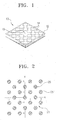
- FIG. 1 illustrates an elevated view of a conventional photonic crystal-based cavity.
- a cavity 10 has a periodic arrangement of air holes 14 and a local defect 16 disrupting the periodic arrangement in a dielectric slab 12 having a predetermined dielectric permittivity.
- the local defect 16 spatially confines electromagnetic fields and generates an electromagnetic mode in a band gap. Further, electromagnetic radiation in a direction vertical to a two-dimensional plane is confined by total internal reflection (TIR).
- TIR total internal reflection
- light incident through a structure having an ordered air hole arrangement 14 and a local defect 16 in the dielectric slab 12 can be captured on a portion of the local defect 16, through which it can be used as a cavity for a laser having a very high quality factor Q.
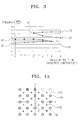
- FIG. 2 illustrates a plan view of a structure of a conventional photonic crystal having a plurality of band gaps.
- a plurality of second dielectric substances 25 having a second dielectric permittivity Inserted in the structure of a photonic crystal having a plurality of band gaps are a plurality of second dielectric substances 25 having a second dielectric permittivity, the second dielectric substances 25 being arranged in a first periodic structure with respect to at least one or more directions on the plane formed by a first dielectric substance 21, e.g., a slab, having a first dielectric permittivity, and a plurality of third dielectric substances 25' having a third dielectric permittivity, the plurality of third dielectric substances 25' being arranged in a second periodic structure in a unit cell formed by the plurality of second dielectric substances 25.
- the plurality of second dielectric substances 25 and the plurality of third dielectric substances 25' are arranged to have a third periodic structure with respect to at least one or more directions.
- the plurality of third dielectric substances 25' can be used with the dielectric permittivity changing while the size thereof is maintained, or, can be used with the size varying while the dielectric permittivity is maintained. Further, the plurality of third dielectric substances 25' can be used while the size and the dielectric permittivity both vary at the same time.
- FIG. 3 is a graph showing respective frequency gaps appearing when the magnitude of a radius of the third dielectric substance 25' varies.
- the photonic crystal includes the plurality of second dielectric substances 25 having a dielectric permittivity of 8.9, a radius R and a lattice constant " a " that are disposed in the first dielectric slab 21 having a dielectric permittivity ⁇ a and the plurality of third dielectric substances 25' having a radius R' that are inserted in the central portions of the unit cells of the lattice structure of the plurality of second dielectric substances 25.
- the radius R' of the third dielectric substance take a value of 0.2 ⁇ 5 2 , 0.4 ⁇ 5 2 , 0.6 ⁇ 5 2 , 0.8 ⁇ 5 2 , and 0.2 ⁇ 2 which come from five equal divisions of a distance from 0 to 0.2 ⁇ 2 .
- the radius R of the plurality of second dielectric substances 25 should be changed to have the five equal divisions between 0.2a and 0.2 ⁇ 2 , as the radius R' of the third dielectric substances 25' changes.
- reference numeral 35' seen from the left, denotes a lower frequency value of a first band gap in the initial photonic crystal, and reference numeral 36' denotes an upper frequency value of the first band gap.
- Reference numeral 31' denotes a frequency at one insertion position where a band gap occurs during the insertions
- reference numeral 31, seen from the right denotes a lower frequency value of the first band gap in a finally inserted photonic crystal
- reference numeral 32 denotes an upper frequency value of the first band gap.
- reference numeral 35 is a frequency value at one insertion position at which the band gap disappears.
- the conventional photonic crystal structure is able to have a plurality of band gaps through the respective insertion of dielectric substances, it is not suitable for use as a cavity. Further, since a cavity using the conventional photonic crystal has a single band gap, it causes a problem in that a resonant mode can be formed only for a single wavelength of a single band.
- a resonant cavity comprising a first dielectric substance having a first dielectric permittivity, a plurality of second dielectric substances each having a second dielectric permittivity, the plurality of second dielectric substances being arranged in a first periodic structure with respect to at least one or more directions on a plane formed of the first dielectric substance, a plurality of third dielectric substances each having a third dielectric permittivity, the plurality of third dielectric substances being arranged in a second periodic structure with respect to at least one or more directions on the plane formed of the first dielectric substance, and being disposed in unit cells formed by the plurality of second dielectric substances so as to be arranged in a third periodic structure together with the plurality of second dielectric substances, and one or more local defects formed to disrupt either the first periodic structure formed by the second dielectric substances or the second periodic structure formed by the third dielectric substances.
- the photonic crystal-based cavity of the invention is capable of forming a plurality of resonant modes with a plurality of band gaps.
- the photonic crystal-based cavity of the invention is also capable of tuning a lasing wavelength of a microlaser.
- the third dielectric substances have the largest possible size that is capable of being inserted in a unit cell formed by the plurality of second dielectric substances without overlapping the second dielectric substances.
- the plurality of third dielectric substances may be additionally disposed on border lines between the unit cells formed by the plurality of second dielectric substances.
- the second dielectric permittivity is greater than the first dielectric permittivity.
- the third dielectric permittivity is greater than the first dielectric permittivity and less than the second dielectric permittivity.
- the one or more defects may be formed by omitting dielectric substances at a predetermined position in the first periodic structure of the plurality of second dielectric substances or in the second periodic structure of the plurality of third dielectric substances.
- the one or more defects may be formed by changing a size or a shape of one or more of the plurality of second dielectric substances at a predetermined position in the first periodic structure of the plurality of second dielectric substances or by changing a size or a shape of one of one or more the plurality of third dielectric substances in the second periodic structure of the plurality of third dielectric substances.
- the photonic crystal-based resonant cavity may further include a waveguide in the first dielectric substance for causing electromagnetic waves to reach the one or more defects.
- a photonic crystal-based resonator having a plurality of filtering frequencies, comprising a cavity having a first dielectric substance having a first dielectric permittivity, a plurality of second dielectric substances each having a second dielectric permittivity, the plurality of second dielectric substances being arranged in a first periodic structure with respect to at least one or more directions on a plane formed of the first dielectric substance, a plurality of third dielectric substances each having a third dielectric permittivity, the plurality of third dielectric substances being arranged in a second periodic structure with respect to at least one or more directions on the plane formed of the first dielectric substance, and being disposed in unit cells formed by the plurality of second dielectric substances so as to be arranged in a third periodic structure together with the plurality of second dielectric substances, and one or more local defects formed to disrupt the first periodic structure formed by the plurality of second dielectric substances or the second periodic structure formed by the plurality of third dielectric substances; a first waveguide
- This aspect of the invention provides a resonator having a plurality of filtering frequencies using a photonic crystal with a plurality of band gaps.
- the first waveguide is an input waveguide for channeling incident electromagnetic waves to the one or more defects.
- the second waveguide is an output waveguide for emitting electromagnetic waves generated by the cavity formed by the one or more defects in a desired output direction.
- the first waveguide and the second waveguide may be formed either on opposite sides of the one or more defects or on the same side of the one or more defects.
- a cavity according to the invention is able to form a plurality of electromagnetic resonant modes having different Q values through a photonic crystal structure having a plurality of band gaps.
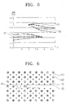
- FIGS. 4A, 4B and 4C illustrate plan views of a structure of a photonic crystal-based cavity according to respective embodiments of the present invention.
- a cavity of FIG. 4A includes a plurality of second dielectric substances 120 arranged in a first periodic structure in a first dielectric substance 110, preferably a first dielectric slab, having a first dielectric permittivity, a plurality of third dielectric substances 130 arranged in a second periodic structure, and a defect 140 disrupting the periodic structure of the plurality of second dielectric substances 120.
- 4B includes the plurality of second dielectric substances 120 arranged in the first periodic structure in the first dielectric slab 110, the plurality of third dielectric substances 130 arranged in the second periodic structure, and a defect 140' disrupting the periodic structure of the plurality of third dielectric substances 130.
- each of the plurality of second dielectric substances 120 have a second dielectric permittivity and each of the plurality of third dielectric substances 130 have a third dielectric permittivity.
- the first dielectric permittivity is less than the second dielectric permittivity
- the third dielectric permittivity has a value that is greater than the first dielectric permittivity and less than the second dielectric permittivity.
- the plurality of third dielectric substances 130 are arranged so that a distance from a center of the third dielectric substance 130 to an outermost edge of the third dielectric substance 130 is smaller than a distance from the center of the third dielectric substance 130 to the second dielectric substances 120 positioned nearest the third dielectric substance 130. That is, the third dielectric substances 130 have the largest possible size that is capable of being inserted in a unit cell formed by the plurality of second dielectric substances 120 without overlapping the second dielectric substances 120.
- the third dielectric substances 130 are arranged in centers of unit cells formed by the second dielectric substances 120.
- the third dielectric substances 130 of FIG. 4C may be positioned, when used, on the border lines between the unit cells formed by the second dielectric substances 120.
- the defects 140, 140' and 140", shown in FIGS. 4A and 4B, respectively are formed by omitting a dielectric substance from the periodic structure of the plurality of second or third dielectric substances 120 and 130. Such an omission to form a defect 140, 140' and 140", however, is not limited to omitting only one dielectric substance.
- the defect 140, 140' and 140" may be formed by omitting a plurality of dielectric substances at a predetermined position from the periodic structures of the second dielectric substances 120 or the third dielectric substances 130. Further, the defects 140, 140' and 140"are formed not only by providing deficiencies in the dielectric substances, but may also be formed by changing a size or a shape of one or more of the dielectric substances of the second and third dielectric substances 120 and 130, respectively, at a predetermined position in the first periodic structure or the second periodic structure, respectively.
- FIG. 5 is a graph showing band gaps and resonant frequencies occurring from the cavities of the FIGS. 4A, 4B and 4C. As compared to FIG. 3, there exist slight differences in band gap positions, but the differences are caused by errors generated during simulations.
- a solid dot line denoted by reference numeral 151 corresponds to resonant frequencies in a band gap formed when one of the plurality of second dielectric substances 120, as shown in FIG. 4A, is missing
- a solid dot line denoted by reference numeral 155 corresponds to resonant frequencies in a band gap formed when one of the plurality of third dielectric substances 130, as shown in FIG. 4B, is missing.
- the other various conditions of the photonic crystal are generally identical to the conditions as shown in FIG. 3.
- the x-axis coordinates are expressed in an exponential power of 1.3 with respect to 0, 1, 2, 3, 4, and 5 obtained from five equal divisions of a distance from 0 to 0.2 ⁇ 2 with reference to a size of the third dielectric substance 130.
- FIG. 5 when one of the plurality of second dielectric substances 120 is missing, as shown in FIG. 4A, a resonant mode is formed only in a low band gap of band gaps when the insertions just started, but, thereafter, a resonant mode begins to form even in the high band gap so that resonant modes exist in both the low and high band gaps. Thereafter as the insertions still progress further, the resonant mode of the low band gap disappears together with the band, and the resonant mode exists only in the high band gap. That is, in the case of the resonant cavity as shown in FIG. 4A, it may be seen that the resonant modes simultaneously exist in the high band gap and the low band gap in the middle of the insertions.
- a resonant mode exists only at the side of the high band gap. That is, with the progress of the insertions, a resonant mode is not formed in the low band gap, but after the high band gap is formed, a resonant mode begins to form from the high band gap. Further, when reached at the last position of the insertions, the resonant mode coincides with the resonant mode for the second dielectric substances 120.
- any one of the plurality of second and third dielectric substances 120 and 130 is missing, a plurality of band gaps exist in the middle positions of the insertions, and electromagnetic resonant modes exist in the low band gap and the high band gap, respectively.
- the positions and quality factor (Q) values of the resonant modes can be adjusted by changing the concrete shapes of the inserted dielectric substances and the shapes of the local defects.
- FIG. 6 illustrates a plan view of a photonic crystal-based resonant cavity according to another embodiment of the present invention.
- a cavity includes the plurality of second dielectric substances 120 arranged in the first periodic structure in the first dielectric slab 110 having a first dielectric permittivity, the plurality of third dielectric substances 130 arranged in the second periodic structure, and a defect 161 disrupting the periodic structure of the plurality of second dielectric substances 120, and a waveguide 165 integrated adjacent to the defect 161 for causing electromagnetic waves to reach the defect 161.
- the cavity as shown in FIG. 6 is used in a semiconductor laser diode and the like so that light emitted from a microlaser through the waveguide 165 can be immediately combined. Further, since a plurality of resonant modes are available in the cavity, the cavity can be applied to a laser diode or the like having a plurality of lasing wavelengths in a set wavelength range.
- FIG. 7A and 7B illustrates a plan view of a photonic crystal-based resonator according to respective embodiments of the present invention.
- the resonator includes a cavity having the plurality of second dielectric substances 120 arranged in the first periodic structure in the first dielectric slab 110 having a first dielectric permittivity, the plurality of third dielectric substances 130 arranged in the second periodic structure, and a defect 171 disrupting the periodic structure of the plurality of second dielectric substances 120; an input waveguide 173 integrated adjacent to the defect 171 so that incident electromagnetic waves can be channeled to the defect 171; and an output waveguide 175 integrated adjacent to the defect 171 so that electromagnetic waves generated by the cavity formed by the defect 171 are emitted in a desired output direction.
- FIG. 7A illustrates the input waveguide 173 and the output waveguide 175 being formed on opposite sides of the defect 171
- the input waveguide 173 and the output waveguide 175 may be formed on the same side of the defect 171.
- the resonator as shown in FIG. 7A and 7B can emit through the output waveguide 175 an electromagnetic wave of a desired wavelength out of electromagnetic wave energy transmitted through the input waveguide 173.
- the resonator has a plurality of resonant modes so that it can be used as a filter or the like that requires the plurality of resonant modes.
- the cavity and resonator using a photonic crystal structure have a plurality of electromagnetic resonant modes available in a plurality of band gaps so that they are able to promote the development of diverse devices, such as a microlaser diode having a plurality of lasing wavelengths finely separated, a resonant filter having a plurality of resonant frequencies, and the like.
Landscapes
- Engineering & Computer Science (AREA)
- Physics & Mathematics (AREA)
- Optics & Photonics (AREA)
- Chemical & Material Sciences (AREA)
- Nanotechnology (AREA)
- Microelectronics & Electronic Packaging (AREA)
- General Physics & Mathematics (AREA)
- Life Sciences & Earth Sciences (AREA)
- Biophysics (AREA)
- Crystallography & Structural Chemistry (AREA)
- Optical Integrated Circuits (AREA)
- Semiconductor Lasers (AREA)
Applications Claiming Priority (2)
| Application Number | Priority Date | Filing Date | Title |
|---|---|---|---|
| KR2002075770 | 2002-12-02 | ||
| KR10-2002-0075770A KR100518835B1 (ko) | 2002-12-02 | 2002-12-02 | 포토닉결정을 이용한 공진기 및 공진장치 |
Publications (2)
| Publication Number | Publication Date |
|---|---|
| EP1426792A2 true EP1426792A2 (de) | 2004-06-09 |
| EP1426792A3 EP1426792A3 (de) | 2005-01-26 |
Family
ID=32310873
Family Applications (1)
| Application Number | Title | Priority Date | Filing Date |
|---|---|---|---|
| EP03257428A Withdrawn EP1426792A3 (de) | 2002-12-02 | 2003-11-25 | Resonanzhohlraum und Resonator aus photonischen Kristallen |
Country Status (4)
| Country | Link |
|---|---|
| US (1) | US7012946B2 (de) |
| EP (1) | EP1426792A3 (de) |
| JP (1) | JP2004310049A (de) |
| KR (1) | KR100518835B1 (de) |
Cited By (2)
| Publication number | Priority date | Publication date | Assignee | Title |
|---|---|---|---|---|
| CN104460174A (zh) * | 2014-12-12 | 2015-03-25 | 南昌航空大学 | 一种基于二维光子晶体的全光二级管的实现方法 |
| CN105022116A (zh) * | 2015-07-24 | 2015-11-04 | 南昌航空大学 | 光子晶体波导侧边双腔全光二极管结构 |
Families Citing this family (11)
| Publication number | Priority date | Publication date | Assignee | Title |
|---|---|---|---|---|
| KR101018376B1 (ko) | 2003-08-22 | 2011-03-02 | 삼성전자주식회사 | 포토닉 밴드갭 광섬유 |
| US7307719B2 (en) * | 2004-09-14 | 2007-12-11 | Hewlett-Packard Development Company, L.P. | Wavelength-tunable excitation radiation amplifying structure and method |
| US7385177B2 (en) * | 2005-01-05 | 2008-06-10 | Ramot At Tel-Aviv University Ltd. | Light guide rotation rate detector with coupled optical resonators |
| US7561761B2 (en) * | 2007-01-03 | 2009-07-14 | Hewlett-Packard Development Company, L.P. | Photonic systems and methods for encoding data in carrier electromagnetic waves |
| KR101025822B1 (ko) * | 2009-06-11 | 2011-03-30 | 한국조폐공사 | 전자기 밴드갭 패턴의 보안코드 인식장치 |
| US9888283B2 (en) | 2013-03-13 | 2018-02-06 | Nagrastar Llc | Systems and methods for performing transport I/O |
| USD758372S1 (en) | 2013-03-13 | 2016-06-07 | Nagrastar Llc | Smart card interface |
| USD864968S1 (en) | 2015-04-30 | 2019-10-29 | Echostar Technologies L.L.C. | Smart card interface |
| KR102384228B1 (ko) | 2015-09-30 | 2022-04-07 | 삼성전자주식회사 | 반도체 레이저 공진기 및 이를 포함하는 반도체 레이저 소자 |
| US11163114B2 (en) * | 2019-08-23 | 2021-11-02 | Globalfoundries U.S. Inc. | Waveguide structures |
| CN117091580A (zh) * | 2022-05-13 | 2023-11-21 | 意子科技私人投资有限公司 | 平面平台上的光机械陀螺仪 |
Citations (2)
| Publication number | Priority date | Publication date | Assignee | Title |
|---|---|---|---|---|
| WO1999064903A1 (en) * | 1998-06-09 | 1999-12-16 | Crystal Fibre A/S | Microstructured optical fibres |
| WO2002012933A2 (en) * | 2000-08-09 | 2002-02-14 | Massachusetts Institute Of Technology | Periodic dielectric structure having a complete three-dimensional photonic band gap |
Family Cites Families (12)
| Publication number | Priority date | Publication date | Assignee | Title |
|---|---|---|---|---|
| US5187461A (en) * | 1991-02-15 | 1993-02-16 | Karl Brommer | Low-loss dielectric resonator having a lattice structure with a resonant defect |
| US5440421A (en) * | 1994-05-10 | 1995-08-08 | Massachusetts Institute Of Technology | Three-dimensional periodic dielectric structures having photonic bandgaps |
| US6058127A (en) * | 1996-12-13 | 2000-05-02 | Massachusetts Institute Of Technology | Tunable microcavity and method of using nonlinear materials in a photonic crystal |
| US6483640B1 (en) * | 1997-04-08 | 2002-11-19 | The United States Of America As Represented By The Secretary Of The Navy | Optical notch filters based on two-dimensional photonic band-gap materials |
| EP1119523B1 (de) * | 1998-07-30 | 2010-11-10 | Corning Incorporated | Verfahren zur herstellung photonischen strukturen |
| JP3407693B2 (ja) * | 1999-06-09 | 2003-05-19 | 日本電気株式会社 | フォトニック結晶 |
| US6532326B1 (en) * | 2000-09-21 | 2003-03-11 | Ut-Battelle, Llc | Transverse-longitudinal integrated resonator |
| US6819691B2 (en) * | 2002-01-28 | 2004-11-16 | The Board Of Trustees Of The Leland Stanford Junior University | Creating sharp asymmetric lineshapes in microcavity structures |
| KR100441507B1 (ko) | 2002-05-06 | 2004-07-23 | 삼성전자주식회사 | 포토닉 결정구조 |
| US6873777B2 (en) * | 2003-03-10 | 2005-03-29 | Japan Aviation Electronics Industry Limited | Two-dimensional photonic crystal device |
| KR100594804B1 (ko) * | 2004-02-19 | 2006-07-03 | 삼성전자주식회사 | 콜로이드 자기조립 광결정의 패턴닝 방법 및 이를 이용한역전된 오팔구조의 3차원 광결정 광도파로 제작방법 |
| US7489846B2 (en) * | 2004-03-11 | 2009-02-10 | Agilent Technologies, Inc. | Photonic crystal sensors |
-
2002
- 2002-12-02 KR KR10-2002-0075770A patent/KR100518835B1/ko not_active Expired - Fee Related
-
2003
- 2003-11-25 EP EP03257428A patent/EP1426792A3/de not_active Withdrawn
- 2003-12-01 JP JP2003401710A patent/JP2004310049A/ja active Pending
- 2003-12-02 US US10/724,632 patent/US7012946B2/en not_active Expired - Lifetime
Patent Citations (3)
| Publication number | Priority date | Publication date | Assignee | Title |
|---|---|---|---|---|
| WO1999064903A1 (en) * | 1998-06-09 | 1999-12-16 | Crystal Fibre A/S | Microstructured optical fibres |
| WO1999064904A1 (en) * | 1998-06-09 | 1999-12-16 | Crystal Fibre A/S | A photonic band gap fibre |
| WO2002012933A2 (en) * | 2000-08-09 | 2002-02-14 | Massachusetts Institute Of Technology | Periodic dielectric structure having a complete three-dimensional photonic band gap |
Cited By (4)
| Publication number | Priority date | Publication date | Assignee | Title |
|---|---|---|---|---|
| CN104460174A (zh) * | 2014-12-12 | 2015-03-25 | 南昌航空大学 | 一种基于二维光子晶体的全光二级管的实现方法 |
| CN104460174B (zh) * | 2014-12-12 | 2017-04-05 | 南昌航空大学 | 一种基于二维光子晶体的全光二极管的实现方法 |
| CN105022116A (zh) * | 2015-07-24 | 2015-11-04 | 南昌航空大学 | 光子晶体波导侧边双腔全光二极管结构 |
| CN105022116B (zh) * | 2015-07-24 | 2017-10-03 | 南昌航空大学 | 光子晶体波导侧边双腔全光二极管结构 |
Also Published As
| Publication number | Publication date |
|---|---|
| US20040120380A1 (en) | 2004-06-24 |
| US7012946B2 (en) | 2006-03-14 |
| KR20040048022A (ko) | 2004-06-07 |
| JP2004310049A (ja) | 2004-11-04 |
| KR100518835B1 (ko) | 2005-10-05 |
| EP1426792A3 (de) | 2005-01-26 |
Similar Documents
| Publication | Publication Date | Title |
|---|---|---|
| US6993235B2 (en) | Three-dimensional periodic structure and functional element including the same | |
| EP1627244B1 (de) | Ringresonator mit radialem bragg-reflektor | |
| US10254478B2 (en) | Integrated impedance-matched photonic zero-index metamaterials | |
| US6624945B2 (en) | Thin film filters using omnidirectional reflectors | |
| EP1426792A2 (de) | Resonanzhohlraum und Resonator aus photonischen Kristallen | |
| US6134043A (en) | Composite photonic crystals | |
| US7085467B2 (en) | Three-dimensional periodic structure, functional element including the same, and light-emitting device | |
| EP1558953B1 (de) | Wellenleiter mit photonischem kristall | |
| CN113866896B (zh) | 一种高q值微环谐振器 | |
| WO2005008296A2 (en) | Optical coupling for whispering-gallery-mode resonators via waveguide gratings | |
| US20090092156A1 (en) | Devices and methods for providing stimulated raman lasing | |
| CN115453690B (zh) | 一种主动模式选择的高q微盘谐振器 | |
| US7502541B2 (en) | Resonator, light emitting device, and wavelength conversion device | |
| CN116053894B (zh) | 一种基于谐振环的全硅太赫兹频移芯片 | |
| CN106680933A (zh) | 一种横向非对称的无反射周期波导微腔带通滤波器 | |
| Kawakami et al. | 3-D photonic-crystal heterostructures: fabrication and in-line resonator | |
| JP3876863B2 (ja) | アド・ドロップフィルタ | |
| US7224868B2 (en) | Radiation-free optical cavity | |
| CN109669240B (zh) | 一种光子晶体波导六极分裂模干涉fano共振结构 | |
| CN109669242A (zh) | 一种光子晶体波导对角模干涉fano共振结构 | |
| JPWO2006103850A1 (ja) | 導波路素子及びレーザ発生器 | |
| Zhang et al. | Generation of Multiple Sharp Fano Resonances based on a Silicon Nanobeam-Microring Resonator | |
| RU161593U1 (ru) | Оптический волноводный фильтр | |
| JP2017151351A (ja) | 光導波路およびドロップフィルタ | |
| CN118033812A (zh) | 一种谐振器 |
Legal Events
| Date | Code | Title | Description |
|---|---|---|---|
| PUAI | Public reference made under article 153(3) epc to a published international application that has entered the european phase |
Free format text: ORIGINAL CODE: 0009012 |
|
| AK | Designated contracting states |
Kind code of ref document: A2 Designated state(s): AT BE BG CH CY CZ DE DK EE ES FI FR GB GR HU IE IT LI LU MC NL PT RO SE SI SK TR |
|
| AX | Request for extension of the european patent |
Extension state: AL LT LV MK |
|
| PUAL | Search report despatched |
Free format text: ORIGINAL CODE: 0009013 |
|
| AK | Designated contracting states |
Kind code of ref document: A3 Designated state(s): AT BE BG CH CY CZ DE DK EE ES FI FR GB GR HU IE IT LI LU MC NL PT RO SE SI SK TR |
|
| AX | Request for extension of the european patent |
Extension state: AL LT LV MK |
|
| 17P | Request for examination filed |
Effective date: 20050413 |
|
| 17Q | First examination report despatched |
Effective date: 20050701 |
|
| AKX | Designation fees paid |
Designated state(s): DE FR GB |
|
| APBN | Date of receipt of notice of appeal recorded |
Free format text: ORIGINAL CODE: EPIDOSNNOA2E |
|
| APBR | Date of receipt of statement of grounds of appeal recorded |
Free format text: ORIGINAL CODE: EPIDOSNNOA3E |
|
| APAF | Appeal reference modified |
Free format text: ORIGINAL CODE: EPIDOSCREFNE |
|
| APBT | Appeal procedure closed |
Free format text: ORIGINAL CODE: EPIDOSNNOA9E |
|
| STAA | Information on the status of an ep patent application or granted ep patent |
Free format text: STATUS: THE APPLICATION IS DEEMED TO BE WITHDRAWN |
|
| 18D | Application deemed to be withdrawn |
Effective date: 20100309 |