EP1426800B1 - Optischer Multiplex/Demultiplex-Schaltkreis mit einem Phasengenerator - Google Patents
Optischer Multiplex/Demultiplex-Schaltkreis mit einem Phasengenerator Download PDFInfo
- Publication number
- EP1426800B1 EP1426800B1 EP03027949A EP03027949A EP1426800B1 EP 1426800 B1 EP1426800 B1 EP 1426800B1 EP 03027949 A EP03027949 A EP 03027949A EP 03027949 A EP03027949 A EP 03027949A EP 1426800 B1 EP1426800 B1 EP 1426800B1
- Authority
- EP
- European Patent Office
- Prior art keywords
- optical
- wavelength
- phase
- phase generating
- demultiplexing
- Prior art date
- Legal status (The legal status is an assumption and is not a legal conclusion. Google has not performed a legal analysis and makes no representation as to the accuracy of the status listed.)
- Expired - Lifetime
Links
Images


Classifications
-
- G—PHYSICS
- G02—OPTICS
- G02B—OPTICAL ELEMENTS, SYSTEMS OR APPARATUS
- G02B6/00—Light guides; Structural details of arrangements comprising light guides and other optical elements, e.g. couplings
- G02B6/10—Light guides; Structural details of arrangements comprising light guides and other optical elements, e.g. couplings of the optical waveguide type
- G02B6/12—Light guides; Structural details of arrangements comprising light guides and other optical elements, e.g. couplings of the optical waveguide type of the integrated circuit kind
- G02B6/12007—Light guides; Structural details of arrangements comprising light guides and other optical elements, e.g. couplings of the optical waveguide type of the integrated circuit kind forming wavelength selective elements, e.g. multiplexer, demultiplexer
- G02B6/12009—Light guides; Structural details of arrangements comprising light guides and other optical elements, e.g. couplings of the optical waveguide type of the integrated circuit kind forming wavelength selective elements, e.g. multiplexer, demultiplexer comprising arrayed waveguide grating [AWG] devices, i.e. with a phased array of waveguides
- G02B6/12019—Light guides; Structural details of arrangements comprising light guides and other optical elements, e.g. couplings of the optical waveguide type of the integrated circuit kind forming wavelength selective elements, e.g. multiplexer, demultiplexer comprising arrayed waveguide grating [AWG] devices, i.e. with a phased array of waveguides characterised by the optical interconnection to or from the AWG devices, e.g. integration or coupling with lasers or photodiodes
-
- G—PHYSICS
- G02—OPTICS
- G02B—OPTICAL ELEMENTS, SYSTEMS OR APPARATUS
- G02B6/00—Light guides; Structural details of arrangements comprising light guides and other optical elements, e.g. couplings
- G02B6/10—Light guides; Structural details of arrangements comprising light guides and other optical elements, e.g. couplings of the optical waveguide type
- G02B6/12—Light guides; Structural details of arrangements comprising light guides and other optical elements, e.g. couplings of the optical waveguide type of the integrated circuit kind
- G02B6/12007—Light guides; Structural details of arrangements comprising light guides and other optical elements, e.g. couplings of the optical waveguide type of the integrated circuit kind forming wavelength selective elements, e.g. multiplexer, demultiplexer
- G02B6/12009—Light guides; Structural details of arrangements comprising light guides and other optical elements, e.g. couplings of the optical waveguide type of the integrated circuit kind forming wavelength selective elements, e.g. multiplexer, demultiplexer comprising arrayed waveguide grating [AWG] devices, i.e. with a phased array of waveguides
- G02B6/12016—Light guides; Structural details of arrangements comprising light guides and other optical elements, e.g. couplings of the optical waveguide type of the integrated circuit kind forming wavelength selective elements, e.g. multiplexer, demultiplexer comprising arrayed waveguide grating [AWG] devices, i.e. with a phased array of waveguides characterised by the input or output waveguides, e.g. tapered waveguide ends, coupled together pairs of output waveguides
-
- G—PHYSICS
- G02—OPTICS
- G02B—OPTICAL ELEMENTS, SYSTEMS OR APPARATUS
- G02B6/00—Light guides; Structural details of arrangements comprising light guides and other optical elements, e.g. couplings
- G02B6/10—Light guides; Structural details of arrangements comprising light guides and other optical elements, e.g. couplings of the optical waveguide type
- G02B6/12—Light guides; Structural details of arrangements comprising light guides and other optical elements, e.g. couplings of the optical waveguide type of the integrated circuit kind
- G02B6/12007—Light guides; Structural details of arrangements comprising light guides and other optical elements, e.g. couplings of the optical waveguide type of the integrated circuit kind forming wavelength selective elements, e.g. multiplexer, demultiplexer
- G02B6/12009—Light guides; Structural details of arrangements comprising light guides and other optical elements, e.g. couplings of the optical waveguide type of the integrated circuit kind forming wavelength selective elements, e.g. multiplexer, demultiplexer comprising arrayed waveguide grating [AWG] devices, i.e. with a phased array of waveguides
- G02B6/12019—Light guides; Structural details of arrangements comprising light guides and other optical elements, e.g. couplings of the optical waveguide type of the integrated circuit kind forming wavelength selective elements, e.g. multiplexer, demultiplexer comprising arrayed waveguide grating [AWG] devices, i.e. with a phased array of waveguides characterised by the optical interconnection to or from the AWG devices, e.g. integration or coupling with lasers or photodiodes
- G02B6/12021—Comprising cascaded AWG devices; AWG multipass configuration; Plural AWG devices integrated on a single chip
-
- G—PHYSICS
- G02—OPTICS
- G02B—OPTICAL ELEMENTS, SYSTEMS OR APPARATUS
- G02B6/00—Light guides; Structural details of arrangements comprising light guides and other optical elements, e.g. couplings
- G02B6/10—Light guides; Structural details of arrangements comprising light guides and other optical elements, e.g. couplings of the optical waveguide type
- G02B6/12—Light guides; Structural details of arrangements comprising light guides and other optical elements, e.g. couplings of the optical waveguide type of the integrated circuit kind
- G02B6/12007—Light guides; Structural details of arrangements comprising light guides and other optical elements, e.g. couplings of the optical waveguide type of the integrated circuit kind forming wavelength selective elements, e.g. multiplexer, demultiplexer
- G02B6/12009—Light guides; Structural details of arrangements comprising light guides and other optical elements, e.g. couplings of the optical waveguide type of the integrated circuit kind forming wavelength selective elements, e.g. multiplexer, demultiplexer comprising arrayed waveguide grating [AWG] devices, i.e. with a phased array of waveguides
- G02B6/12023—Light guides; Structural details of arrangements comprising light guides and other optical elements, e.g. couplings of the optical waveguide type of the integrated circuit kind forming wavelength selective elements, e.g. multiplexer, demultiplexer comprising arrayed waveguide grating [AWG] devices, i.e. with a phased array of waveguides characterised by means for reducing the polarisation dependence, e.g. reduced birefringence
-
- G—PHYSICS
- G02—OPTICS
- G02B—OPTICAL ELEMENTS, SYSTEMS OR APPARATUS
- G02B6/00—Light guides; Structural details of arrangements comprising light guides and other optical elements, e.g. couplings
- G02B6/24—Coupling light guides
- G02B6/26—Optical coupling means
- G02B6/28—Optical coupling means having data bus means, i.e. plural waveguides interconnected and providing an inherently bidirectional system by mixing and splitting signals
- G02B6/293—Optical coupling means having data bus means, i.e. plural waveguides interconnected and providing an inherently bidirectional system by mixing and splitting signals with wavelength selective means
- G02B6/29346—Optical coupling means having data bus means, i.e. plural waveguides interconnected and providing an inherently bidirectional system by mixing and splitting signals with wavelength selective means operating by wave or beam interference
- G02B6/2935—Mach-Zehnder configuration, i.e. comprising separate splitting and combining means
- G02B6/29352—Mach-Zehnder configuration, i.e. comprising separate splitting and combining means in a light guide
- G02B6/29353—Mach-Zehnder configuration, i.e. comprising separate splitting and combining means in a light guide with a wavelength selective element in at least one light guide interferometer arm, e.g. grating, interference filter, resonator
-
- G—PHYSICS
- G02—OPTICS
- G02B—OPTICAL ELEMENTS, SYSTEMS OR APPARATUS
- G02B6/00—Light guides; Structural details of arrangements comprising light guides and other optical elements, e.g. couplings
- G02B6/24—Coupling light guides
- G02B6/26—Optical coupling means
- G02B6/28—Optical coupling means having data bus means, i.e. plural waveguides interconnected and providing an inherently bidirectional system by mixing and splitting signals
- G02B6/293—Optical coupling means having data bus means, i.e. plural waveguides interconnected and providing an inherently bidirectional system by mixing and splitting signals with wavelength selective means
- G02B6/29346—Optical coupling means having data bus means, i.e. plural waveguides interconnected and providing an inherently bidirectional system by mixing and splitting signals with wavelength selective means operating by wave or beam interference
- G02B6/2935—Mach-Zehnder configuration, i.e. comprising separate splitting and combining means
- G02B6/29352—Mach-Zehnder configuration, i.e. comprising separate splitting and combining means in a light guide
- G02B6/29355—Cascade arrangement of interferometers
-
- G—PHYSICS
- G02—OPTICS
- G02B—OPTICAL ELEMENTS, SYSTEMS OR APPARATUS
- G02B6/00—Light guides; Structural details of arrangements comprising light guides and other optical elements, e.g. couplings
- G02B6/24—Coupling light guides
- G02B6/26—Optical coupling means
- G02B6/28—Optical coupling means having data bus means, i.e. plural waveguides interconnected and providing an inherently bidirectional system by mixing and splitting signals
- G02B6/293—Optical coupling means having data bus means, i.e. plural waveguides interconnected and providing an inherently bidirectional system by mixing and splitting signals with wavelength selective means
- G02B6/29379—Optical coupling means having data bus means, i.e. plural waveguides interconnected and providing an inherently bidirectional system by mixing and splitting signals with wavelength selective means characterised by the function or use of the complete device
- G02B6/2938—Optical coupling means having data bus means, i.e. plural waveguides interconnected and providing an inherently bidirectional system by mixing and splitting signals with wavelength selective means characterised by the function or use of the complete device for multiplexing or demultiplexing, i.e. combining or separating wavelengths, e.g. 1xN, NxM
Definitions
- the present invention relates to an optical multi/demultiplexing circuit used in an optical communication field, and particularly to an optical multi/demultiplexing circuit used for wavelength division multiplexing.
- the guided-wave optical branching component is composed of Mach-Zehnder interferometer having two or more directional couplers.
- a slight difference ⁇ L in the optical-path length is given to the two or more optical wave-guides connecting the two or more directional couplers.
- the difference of the optical-path length is determined less than the shortest wavelength in the operational wavelength region of the guided-wave optical branching component, and a coupling ratio of each of the two directional couplers is determined to monotonically increase according to the wavelength in the operational wavelength region.
- Mach-Zehnder interferometer type 3-dB optical coupler Mach-Zehnder interferometer type 3-dB optical coupler
- MZI Mach-Zehnder interferometer
- document EP 1 231 490 A2 discloses an optical multiplexer and an optical demultiplexer. Specifically, the optical demultiplexer and the optical multiplexer provide the transmission characteristics of which are unlikely to be affected by fabrication errors and which have small group delay dispersion.
- a cross output port of a second optical demultiplexer element is selected, and a through output port of a third DEMUX is selected.
- a T-OUT of a first DEMUX has a passband equal to the X-OUT of the second DEMUX, and a X-OUT of the first DEMUX has a passband equal to the T-OUT of the third DEMUX.
- the T-OUT of the first DEMUX has group delay characteristics opposite to those of the X-out of the second DEMUX, and the X-OUT of the first DEMUX has group delay characteristics opposite to those of the T-OUT of the third DEMUX.
- polarization independent optical isolator/circulator devices are based on Mach-Zehnder interferometers.
- the devices utilize either polarization splitting and non-reciprocal polarization conversion or non-reciprocal phase shift within the interferometric arm.
- the relative phase difference is 0° in the forward propagation direction and 180° in the backward propagation direction, or vice versa, so that light goes into a bar or cross port depending on the propagation direction.
- the devices have advantages over previous designs in the use of inexpensive device components, simple alignment, minimal space-requirement, and negligible polarization mode dispersion or polarization dependent loss.
- the devices can be made in a waveguide form with minimal loss and with high fabrication ease.
- An additional phase compensator and/or a variable attenuator can be integrated in order to relax the fabrication tolerances.
- a polarization state changer and a phase shifter for shifting a phase of an optical signal including a waveguide having a waveguiding region for guiding the optical signal therethrough, a substrate for supporting said waveguide, and means for inducing stress on the waveguiding region for shifting the phase of the optical signal are provided.
- the stress is induced by MEMS means.
- the MEMS means are monolithically formed on the substrate and can be actuated by electrostatical force, mechanical force, or tilt-able flaps.
- the optical switching apparatus includes a Mach-Zehnder interferometer.
- the Mach-Zehnder interferometer includes first and second optical signal ports coupled to first and second optical paths by a coupler.
- the first path includes a plurality of phase modulators to selectively provide phase shifts on a wavelength component basis.
- the phase modulators are used to selectively couple optical signals from the input port and add port to the output port on a wavelength component by wavelength component basis.
- document EP 1 168 010 A2 discloses an optical multi/demultiplexer that has a wide passband and small crosstalk among its all channels. It includes first and second arrayed waveguide gratings and a 2x2 optical signal processor.
- the 2x2 optical signal processor includes first to fourth directional couplers, and first to third delay lines.
- the first to third delay lines have thin film heater phase shifters for correcting phase errors involved in fabrication. Utilizing the 2x2 optical signal processor having a transmission spectrum with a square profile having a wide passband and rejection band makes it possible for the optical multi/demultiplexer that combines the arrayed waveguide gratings with the waveguide type circulating filter (2x2 optical signal processor) to widen the extinction bandwidth of the adjacent channel.
- document Xp-001158312 discloses a stabilized coupler in the form of a compact and high performance waveguide-type interleave filters for WDM networks. Specifically, ways of improving the performance of waveguide-type interleave filters are described. These techniques are designed to stabilize the coupling ratio and reduce the chip size.
- DWDM dense wavelength division multiplexing
- an arrayed waveguide grating and lattice-form filter see, for example, M. Oguma et al., "Passband-width broadening design for WDM filter with lattice-form interleave filter and arrayed-waveguide gratings", IEEE Photonics Technology Letters 2002, Vol. 14, pp. 328-330 ); an asymmetric Mach-Zehnder interferometer (see, for example, De Merlier et al., "All-optical 2R regeneration based on integrated asymmetric Mach-Zehnder interferometer incorporating MMI-SOA", Electronics Letters 2002, Vol.
- a symmetric Mach-Zehnder interferometer see, for example, Y. Hashizume et al., "Integrated polarization beam splitter using waveguide birefringence dependence on waveguide core width", Electronics Letters 2001, Vol. 37, pp. 1517-1518 ); a cascaded Mach-Zehnder interferometer (see, for example, K. Suzuki et al., "PLC-based dynamic gain equalizer consisting of integrated Mach-Zehnder interferometers with C- and L-band equalizing range", Electronics Letters 2002, Vol. 38, pp. 1030-1031 ); and a transversal-form filter (see, for example, T. Mizuno et al., "Dispersionless interleave filter based on transversal form optical filter” Electronics Letters 2002, Vol. 38, pp. 1121-1122 ).
- the wavelength grid of such a CWDM system has a uniform wavelength period of 20 nm. Accordingly, the optical devices for the CWDM system must be designed to have the passband with uniform wavelength period.
- the transmittance spectra of the conventional optical multi/demultiplexing circuits such as Mach-Zehnder interferometers have a uniform frequency period, its wavelength characteristics do not become periodic on a uniform wavelength axis. Consequently, they are not applicable to the CWDM systems because of their variations in an insertion loss, passband width and extinction ratio depending on the wavelength grid.
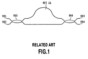
- Fig. 1 shows a conventional Mach-Zehnder interferometer as a concrete example.
- the Mach-Zehnder interferometer consists of two optical couplers 905 and 906, an optical delay line section 907 between the two optical couplers, and two input/output optical waveguides connected to the optical couplers 905 and 906 (see, for example, K. Okamoto, "Fundamentals of optical waveguides” Academic Press 2000, pp. 159-161 ).
- the optical couplers 905 and 906 directional couplers are used whose power coupling ratio is set at 50%.
- the Mach-Zehnder interferometer is a multi/demultiplexing circuit with uniform frequency period as will be described below.
- the two optical output powers of the Mach-Zehnder interferometer are given by the following expressions.
- 2
- 2
- n a refractive index
- ⁇ L a path length difference
- f a frequency
- c the speed of light
- ⁇ the wavelength
- m an integer
- the frequency period are given by the following expression using the foregoing expression (3) considering that the squares of cosine and sine functions have a period n.
- the frequency period become constant, which means that the Mach-Zehnder interferometer constitutes a multi/demultiplexing circuit with uniform frequency period.
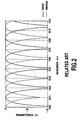
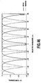
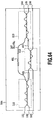
- Fig. 2 illustrates transmission characteristics when the central wavelength of the Mach-Zehnder interferometer is set at 1470 nm, and the optical path length difference through the optical delay line section is set at 55.9 ⁇ m that gives the frequency period of 20 nm as the demultiplexing period between the through port and cross port near the central wavelength.
- the horizontal axis represents wavelength, on which the wavelength grid is arranged at uniform period; the solid lines represents the transmission characteristics of the optical signal output from the cross port; and the broken lines represents the transmission characteristics of the optical signal output from the through port.
- Fig. 3 illustrates transmission characteristics when the horizontal axis represents the optical frequency for comparison purposes.
- the Mach-Zehnder interferometer has transmission characteristics with uniform frequency period rather than with uniform wavelength period.
- the demultiplexing periods of the through port and cross port are 20 nm near 1470 nm, and hence agree with the wavelength grid, the wavelength periods increase as they move from 1470 nm toward a longer wavelength side, thereby departing from the wavelength grid clearly. Therefore these optical devices are inappropriate for use in the CWDM system because their insertion loss, passband width and extinction ratio vary greatly depending on the wavelength grid.
- the interferometers with the conventional configurations such as the Mach-Zehnder interferometer do not have a uniform wavelength period, they present a problem in that their passband deviates from the grid on the wavelength axis as the passband departs from the central wavelength, and that the insertion losses vary remarkably depending on the wavelength.
- a conventional optical multi/demultiplexing circuit has a uniform period in the optical frequency domain, and its transmission characteristics are characterized by the optical frequency period and the central optical frequency.
- the conventional optical multi/demultiplexing circuit has only one design parameter that can be set freely in connection with the optical frequency period and central optical frequency: that is, the optical path length difference of the optical delay line. Therefore, the optical frequency period and the center optical frequency could not be set simultaneously.
- the optical multi/demultiplexing circuit which has the uniform frequency period in principle, cannot set the optical frequency period and the central optical frequency at the same time, thereby offering a problem of deteriorating the transmission characteristics even when it is used in the optical frequency domain.
- an optical delay line usually implements the path length difference, it can also be implemented by utilizing a phase difference of optical signals output from an optical coupler. For example, if we suppose that there is a phase difference of 2 ⁇ when optical signals are output from a certain optical coupler, it will correspond to a path length difference of one wavelength. Therefore, if an optical coupler, whose output phase difference has wavelength dependence, can be devised, a path length difference corresponding to the amount of deviation from the wavelength grid can be provided to the optical delay line.
- the conventional optical coupler such as a directional coupler and multimode interferometer used in the conventional technique, however, cannot provide a path length difference ⁇ L with wavelength dependence. This is because the phase difference of the optical signals output from its outputs is constant, thereby being unable to cause any phase difference depending on the wavelength.
- an object of the present invention is to provide an optical multi/demultiplexing circuit with uniform wavelength period whose center of passbands agrees with the grid on the wavelength axis.
- an "optical multi/demultiplexing device” refers to a circuit configured by optical couplers and optical delay lines device; a "phase generating device” refers to a device for generating a phase ⁇ ; and a “phase generating optical coupler” refers to a circuit functioning as the phase generating device and optical multi/demultiplexing device.
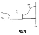
- Fig. 4 shows a first embodiment of the optical multi/demultiplexing circuit.
- the present embodiment includes two two-input/two-output phase generating optical couplers 111 and 112; an optical delay line section 107 consisting of two optical waveguides between the two phase generating optical couplers 111 and 112; and two input/output optical waveguides 101 and 102, and 103 and 104 connected to the phase generating optical couplers 111 and 112.
- the optical multi/demultiplexing circuit has a function (phase generating function) for correcting the deviation of the wavelength period so that the transmission characteristics have an approximately uniform period on the wavelength axis.
- the function can be achieved by configuring at least one of the phase generating optical couplers 111 and 112 in such a fashion that the output phase difference of the phase generating optical coupler has a wavelength dependence in the passband of the optical multi/demultiplexing circuit.
- a function is also achievable by installing on the optical waveguides of the optical delay line section 107 a phase generating device capable of generating a phase that has a wavelength dependence.
- phase correction will be described in a more detail.
- Fig. 5 illustrates general relationships between the wavelength and frequency.
- a frequency period ⁇ f1 ( ⁇ 2.74 THz) near 1470 nm is obtained, and frequencies are plotted in a uniform period of ⁇ f1 with reference to the frequency at 1470 nm, which is labeled as "uniform frequency period 1".
- the deviation is divided into a linear section and a nonlinear section.
- a method will be described for correcting the linear section of the deviation between the uniform wavelength period and uniform frequency period 1.
- a frequency period ⁇ f2 ( ⁇ 2.53 THz) is obtained as the average value of the frequency period near 1470 nm and the frequency period near 1610 nm.
- the frequencies are plotted in a uniform period of ⁇ f2 with reference to the frequency at 1470 nm, which is labeled as "uniform frequency period 2" as illustrated in Fig. 6.
- the uniform wavelength period and uniform frequency period 2 agree with each other near 1470 nm, deviate slightly as they proceed toward the longer wavelength side, and agree again near 1610 nm. This proves that the deviation between the uniform wavelength period and uniform frequency period can be corrected substantially by the correction in the linear section.
- Fig. 7 shows a Mach-Zehnder interferometer in which the linear section of the deviation between the uniform wavelength period and uniform frequency period is corrected.
- the circuit includes two optical couplers 201 and 301; an optical delay line section 107 between the two optical couplers 201 and 301; and two input/output optical waveguides 101 and 102, and 103 and 104 connected to the optical couplers 201 and 301, respectively.
- the optical couplers 201 and 301 directional couplers with the power coupling ratio of 50% are used.
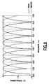
- Fig. 8 illustrates the wavelength dependence of the transmission characteristics in this case.
- the center of the passbands are exactly on the grid at both ends although it deviates slightly at the middle of the wavelength axis.
- the transmittance on the wavelength grid is high at both ends of the wavelength region, thereby being able to reduce the crosstalk and improve the characteristics.
- the linear section of the deviation between the uniform wavelength period and uniform frequency period can be corrected by providing the optical delay line with an additional path length of the wavelength order.
- the central section on the wavelength axis still has slight deviation.
- a method will be described for correcting the nonlinear section of the deviation between the uniform wavelength period and uniform frequency period by using a phase generating optical coupler.
- Fig. 9 illustrates, for the individual wavelengths on the CWDM grid, a plot of the values obtained by dividing the frequency deviation between the uniform wavelength period and uniform frequency period 2 illustrated in Fig. 6 by a frequency period ⁇ f2, that is, the amount of phase necessary for correcting the nonlinear section of the deviation between the uniform wavelength period and uniform frequency period.
- ⁇ f2 the frequency period necessary for correcting the nonlinear section of the deviation between the uniform wavelength period and uniform frequency period.
- the second term and the third term onward represent the linear section and nonlinear section in the relationships between the wavelength and frequency, respectively. Accordingly, using a nonlinear polynomial, especially, a quadratic function or a function of a higher order can give good approximation of the phase required to correct the deviation between the uniform wavelength period and uniform frequency period.
- the curve of Fig. 9 is approximated as follows by the phase ⁇ as a result of a multiple regression analysis. ⁇ ⁇ 8.12 ⁇ 10 - 6 ⁇ ⁇ 2 - 0.025 ⁇ ⁇ + 19.2
- phase correction amount ⁇ ⁇ ⁇ 0.122 - 37.94 186.5 ⁇ 0.5 ⁇ ⁇ ⁇ exp - 2 ( ⁇ - 1539.54 ⁇ ) 2 186.5 2
- a phase generating optical coupler is used, which creates a phase with wavelength dependence in the passbands of the interferometer (1470-1610 nm in the present embodiment), using the difference of the phase output from the two output ports.
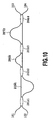
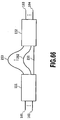
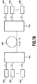
- Fig. 10 shows a configuration of the phase generating optical coupler whose output phase difference varies in the passbands of the multi/demultiplexing circuit.
- the phase generating optical coupler comprises four optical couplers 201-204, and three optical delay line sections 205-207 interposed between the adjacent optical couplers 201-204. It is possible to set the power coupling ratio of the phase generating optical coupler and the wavelength dependence of the output phase difference by determining the power coupling ratios of the four optical couplers 201-204 and by providing the three optical delay lines 205-207 with appropriate path length differences.
- the optical couplers 201, 202, 203 and 204 directional couplers with the power coupling ratios r1, r2, r3 and r4 are used, respectively.
- the path length differences of the optical delay lines 205, 206 and 207 are set at ⁇ 1, ⁇ 2 and ⁇ 3.
- the phase generating optical coupler includes three optical delay lines (or four optical couplers), the number of the optical delay lines may be two or four. As the number of the optical delay lines increases, the flexibility of controlling the phase characteristics of the phase generating optical coupler increases, thereby improving the accuracy of the fitting . However, as the number of the optical delay lines increases, the size of the circuit increases as well. Accordingly, it is preferable that the phase generating optical coupler be configured using the minimum number of the optical delay lines that can achieve a sufficient degree of approximation. More specifically, if the number of the optical delay lines exceeds six (or the number of the optical couplers exceeds seven), the size of the circuit becomes too large. Consequently, the number of the optical delay lines is preferably set equal to or less than six.
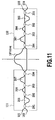
- An interferometer suitable for the present embodiment includes two optical multiplexing sections 111 and 112 which are interconnected through the optical delay line 107 as shown in Fig. 11, and include three optical delay lines (205, 206 and 207, and 305, 306 and 307) each.
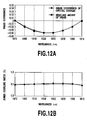
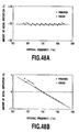
- FIG. 12A is a graph illustrating the wavelength dependence of the phase difference between the optical signals output from the two output ports of the two optical couplers (phase generating optical couplers) of the asymmetric Mach-Zehnder interferometer; and Fig. 12B illustrates the wavelength dependence of the power coupling ratio.
- the variation in the path length per phase difference of 2 ⁇ is 1 ⁇ c, where ⁇ c is the central wavelength, and the path length difference is represented in terms of the relative path length of one of the waveguides (lower waveguide of Fig.
- phase generating optical couplers on both sides of the asymmetric Mach-Zehnder interferometer can be used to provide different amount of phase, or that only the phase generating optical coupler on one side can be used to carry out the phase correction.
- a conventional optical coupler whose output phase difference is constant can be used
- the phase generating optical coupler 112 a phase generating optical coupler whose output phase difference is wavelength dependent in the passbands of the multi/demultiplexer can be used (for example, the phase generating optical coupler including six optical delay lines (or seven optical couplers) can be used).
- the phase generating optical coupler 112 alone can be used to compensate for the phase difference as illustrated in Fig. 12A while the power coupling ratio is set as illustrated in Fig. 12B with offering similar advantages.
- the uniform wavelength period circuit can also be implemented by the configuration in which the interferometer includes only one phase generating optical coupler whose output phase difference has the wavelength dependence.
- the phase difference between the optical signals which are output from the two output ports of the phase generating optical coupler with the configuration as illustrated in Fig. 10
- the phase difference of the phase generating optical coupler agree with the amount of phase necessary for the correction of the nonlinear section of the deviation between the uniform wavelength period and uniform frequency period.
- the wavelength dependence of the power coupling ratio of the phase generating optical coupler is small, it is expected that the wavelength dependence is small for the transmission characteristics of the multi/demultiplexing circuit using the phase generating optical coupler.
- Fig. 13 illustrates the wavelength dependence of the transmission characteristics in the case where the phase generating optical couplers as illustrated in Fig. 10 are used as the two phase generating optical couplers 111 and 112 that constitute the multi/demultiplexing circuit of Fig. 4.
- the two phase generating optical couplers are placed in left-right symmetry with respect to the middle line (broken line of Fig. 11) of the optical delay line 107 as illustrated in Fig. 11 so that the phase differences given by the two phase generating optical coupler is added.
- the linear section of the deviation between the uniform wavelength period and uniform frequency period is corrected through the optical delay line.
- the nonlinear section of the deviation between the uniform wavelength period and uniform frequency period is corrected by the phase generating optical couplers whose output phase differences have a wavelength dependence.
- the center of the passbands are placed on the CWDM grid throughout the wavelength range. Since the wavelength dependence of the transmission characteristics is small, low crosstalk are achieved throughout the wavelength range.
- the optical multi/demultiplexing circuit was fabricated by forming silica-based optical waveguides on a silicon substrate using flame hydrolysis deposition, photolithography and reactive ion etching.
- the relative refractive index difference of the waveguides was 0.75%
- the core thickness of the waveguides was 7 ⁇ m
- the core width was 7 ⁇ m.
- the fabricated wafer was cut, and optical fibers were connected to the circuit to assemble a module. Since the wavelength dependence of the refractive index of the waveguide materials used in the present embodiment was small in the wavelength band, the refractive index was assumed to be constant.
- optical multi/demultiplexing circuit is described by way of example with a minimum configuration for implementing the optical device, it is also possible to take a configuration for reducing the polarization dependence or temperature dependence of the optical multi/demultiplexing circuit.
- optical multi/demultiplexing circuit enables the implementation of the optical device with the uniform wavelength period.
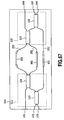
- Fig. 14 shows a second embodiment of the optical multi/demultiplexing circuit.
- the present embodiment includes two phase generating optical couplers 111 and 112 whose output phase differences have a wavelength dependence in the passband; an optical delay line section 107 between the two phase generating optical couplers 111 and 112; and two input/output optical waveguides 101 and 102, and 103 and 104 connected to the phase generating optical couplers 111 and 112, respectively.
- the two phase generating optical couplers 111 and 112 are each configured as shown in Fig. 15. They include four optical couplers 201-204, and three optical delay line sections 205-207 between the adjacent optical couplers 201-204.
- the multi/demultiplexing circuit has the transmission characteristics with approximately uniform period on the wavelength axis.
- the deviation between the uniform wavelength period and uniform frequency period is corrected by the optical delay line and the phase generating optical couplers whose phase differences between the outputs vary within the passband of the multi/demultiplexing circuit.
- the characteristics of an optical interferometer generally depends on the path lengths of the optical delay line section. Thus, if the path lengths deviate from the designed values because of fabrication errors, the desired characteristics cannot be achieved.
- the present embodiment of the optical multi/demultiplexing circuit includes a path length difference adjusting device formed on the optical delay line to improve the accuracy of the path lengths of the optical delay line section.
- optical delay line sections 205-207 of the phase generating optical couplers constituting the Mach-Zehnder interferometer as shown in Fig. 15 include path length difference adjusting devices 401 so that they can vary the path length differences ⁇ 1, ⁇ 2 and ⁇ 3 by the path length adjustment.
- optical couplers 201, 202, 203 and 204 constituting the phase generating optical couplers 111 and 112 that provide such phase characteristics
- the deviation between the uniform wavelength period and uniform frequency period was corrected as illustrated in Fig. 13, thereby being able to match the transmission characteristics approximately to the CWDM grid throughout the wavelength range.
- the wavelength dependence of the transmission characteristics is small, the crosstalk are low throughout the wavelength range.
- the present embodiment includes the path length difference adjusting devices in the optical delay line, they can be used to vary the optical path lengths freely.
- the path length differences of the optical delay lines that constitute the phase generating couplers can be initially set at 0, and after fabricating the circuit, they can be set at certain values using the path length difference adjusting devices.
- the path length adjustment can be carried out for one of the pair of waveguides in the optical delay line as illustrated in Fig. 16, or for both of them as illustrated in Fig. 17.
- the path length difference adjusting devices can be provided to a plurality of places of the same waveguide as illustrated in the optical delay line 107 of Fig. 16. Furthermore, the geometry and positions of the path length difference adjusting devices can be set freely.
- path lengths can be set at certain values by providing the path length differences in advance as shown in Fig. 15, and then by adjusting the path length using the path length difference adjusting devices.
- the optical multi/demultiplexing circuit was fabricated by forming silica-based optical waveguides composed of an undercladding 503, cores 502 and an overcladding 501 on a silicon substrate 504 using flame hydrolysis deposition, photolithography and reactive ion etching.
- thin film heaters were formed are the optical waveguides to use them as path length difference adjusting devices 401.
- the optical multi/demultiplexing circuit was fabricated in such a manner that the relative refractive index difference of the waveguides was 0.75%, the core thickness of the waveguides was 7 ⁇ m, and the core width was 7 ⁇ m.
- the fabricated wafer was cut, and optical fibers were connected to the circuit to assemble a module.
- the optical path length differences of the optical delay lines were adjusted by changing the refractive index of the waveguides by the local heat treatment method involving thin film heaters.
- path length difference adjusting devices 401 are described by way of example using the thermooptic effect by the thin film heaters, other methods can be used. For example, it is also possible to use light irradiation with a laser, electro-optic effect, magnetooptic effect or any other means that can carry out the path length adjustment.
- the refractive index of the waveguide materials used in the present embodiment was small in the wavelength band, the refractive index was assumed to be constant. However, when the wavelength dependence of the refractive index is large, the relationship between the uniform wavelength period and uniform frequency period in Fig. 6 changes. In such a case, however, it is possible to correct the deviation between the uniform wavelength period and uniform frequency period together with the wavelength dependence of the refractive index as in the case where the refractive index is constant, by deriving the required amount of phase considering the wavelength dependence of the refractive index, and by appropriately determining the phase characteristics of the phase generating optical coupler for example using least square approximation.
- optical multi/demultiplexing circuit is described by way of example with a minimum configuration for implementing the optical device, it is also possible to take a configuration for reducing the polarization dependence or temperature dependence of the optical multi/demultiplexing circuit.
- the present embodiment employs the path length difference adjusting devices such as thin film heaters, and uses them to adjust the optical path length difference of the optical delay line by varying the refractive index of the waveguides, thereby reducing the effect of the fabrication errors.
- the optical path length differences of the optical delay lines that constitute the multi/demultiplexing circuit can be set exactly at the designed values by operating the path length difference adjusting devices.
- the present embodiment can implement the optical multi/demultiplexing circuit with the uniform wavelength period.
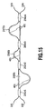
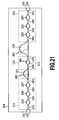
- Fig. 19 shows a third embodiment of the multi/demultiplexing circuit.
- the circuit includes three phase generating optical couplers 111 , 112 and 113 ; two optical delay line sections 107 and 108 between the three phase generating optical couplers; two input/output optical waveguides 101 and 102 connected to the phase generating optical coupler 111; and two input/output optical waveguides 103 and 104 connected to the phase generating optical coupler 113.
- At least one of the three optical multi/demultiplexing devices consists of a phase generating optical coupler, and the phase difference between the outputs varies corresponding to wavelength in the passband of the interferometer, thereby equipped with a the phase generating function.
- the first and second embodiments are an optical multi/demultiplexer with the phase generating function based on the conventional Mach-Zehnder interferometer
- the method as described in the first embodiment can implement the optical multi/demultiplexing circuit with the uniform wavelength period from the optical multi/demultiplexing circuit with the uniform frequency period.
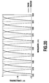
- Fig. 20 illustrates the wavelength dependence of the transmission characteristics of the present embodiment of the optical multi/demultiplexing circuit.
- the optical multi/demultiplexing circuit corrects the deviation between the uniform wavelength period and uniform frequency period by using the phase generating optical couplers whose output phase differences varies corresponding to wavelength in the passbands of the optical multi/demultiplexing circuit, thereby implementing the optical multi/demultiplexing circuit with uniform period on the wavelength axis.
- a phase generating optical coupler can be used which includes M + 1 optical couplers, and M optical delay line sections between the adjacent optical couplers, where M is an integer equal to or greater than two.
- the optical multi/demultiplexing circuit of Fig. 21 employs the phase generating optical couplers as illustrated in Fig. 10 as the phase generating optical couplers 111 and 113, and a Mach-Zehnder-type optical coupler as the phase generating optical coupler 112.
- the optical delay lines of the present embodiment of the optical multi/demultiplexing circuit can comprise a path length difference adjusting device.
- the optical path length differences of the optical delay lines that constitute the phase generating optical couplers can initially be set at zero, and after fabricating the circuit, they can be set at certain values using the path length difference adjusting devices.
- path lengths can be set at certain values by providing the path length differences in advance as shown in Fig. 15, and then by using the path length difference adjusting devices.
- phase generating optical coupler 112 function as a Mach-Zehnder-type optical coupler with a variable power coupling ratio by adjusting the path length difference of the optical delay line.
- the optical multi/demultiplexing circuit was fabricated by forming silica-based optical waveguides composed of an undercladding 503, cores 502 and an overcladding 501 on a silicon substrate 504 using flame hydrolysis deposition, photolithography and reactive ion etching as described before in connection with Fig. 18.
- thin film heaters were formed over the optical waveguides to use them as path length difference adjusting devices 401.
- the relative refractive index difference of the waveguides was 0.75%
- the core thickness of the waveguides was 7 ⁇ m
- the core width was 7 ⁇ m.
- the fabricated wafer was cut, and optical fibers were connected to the circuit to assemble a module.
- the optical path length differences of the optical delay lines were adjusted by changing the refractive index of the waveguides by the local heat treatment method involving thin film heaters.
- path length difference adjusting devices 401 are described by way of example using the thermooptic effect by the thin film heaters, other methods can be used. For example, it is also possible to use light irradiation with a laser, electro-optic effect, magnetooptic effect or any other means that can carry out the path length adjustment.
- the refractive index of the waveguide materials used in the present embodiment was small in the wavelength band, the refractive index was assumed to be constant. However, when the wavelength dependence of the refractive index is large, the relationship between the uniform wavelength period and uniform frequency period in Fig. 6 changes. In such a case, however, it is possible to correct the deviation between the uniform wavelength period and uniform frequency period together with the wavelength dependence of the refractive index as in the case where the refractive index is constant by deriving the required amount of phase considering the wavelength dependence of the refractive index, and by appropriately determining the phase characteristics of the phase generating optical couplers for example using nonlinear polynomial approximation.
- optical multi/demultiplexing circuit is described by way of example with a minimum configuration for implementing the optical device, it is also possible to take a configuration for reducing the polarization dependence or temperature dependence of the optical multi/demultiplexing circuit.
- the present embodiment can be applied to a lattice-form filter to demonstrate applicability to any conventional interferometers other than the Mach-Zehnder interferometer.
- devices other than the lattice-form filter such as a cascaded Mach-Zehnder interferometer, transversal-form filter, and other interferometers can be used.
- it is applicable not only to interferometers with one-input/two-outputs, but also to interferometers with a desired number of inputs/outputs.
- the present embodiment can implement the optical multi/demultiplexing circuit with the uniform wavelength period by using the multi/demultiplexing circuit of the present embodiment.
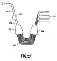
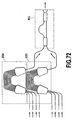
- Fig. 22 shows a fourth embodiment of the optical multi/demultiplexing circuit.
- the circuit comprises an interferometer and an arrayed waveguide grating.
- the interferometer includes two phase generating optical couplers 111 and 112, an optical delay line section 107 between the two phase generating optical couplers, and input waveguides 101 and 102 connected to the phase generating optical coupler 111.
- the arrayed waveguide grating includes array waveguides 603, a first slab waveguide 602 and a second slab waveguide 604 disposed on both sides of the array waveguides, and eight output waveguides 605 connected to the second slab waveguide.
- the two outputs of the phase generating optical coupler 112 of the interferometer are launched into the first slab waveguide 602 of the arrayed waveguide grating.
- the geometry of the contacts can take any form.
- optical waveguides whose geometry varies such as tapered waveguides can be connected to the slab waveguide.
- At least one of the optical multi/demultiplexing devices consists of a phase generating device that produces an output phase difference corresponding to a wavelength in the passbands of the optical multi/demultiplexing circuit, and at the same time functions as an optical coupler, that is, a phase generating optical coupler.
- the present embodiment of the optical multi/demultiplexing circuit is based on a configuration in which the two outputs of a conventional Mach-Zehnder interferometer are launched into a first slab waveguide of an arrayed waveguide grating (see, Fig. 6 of Japanese patent application laid-open No. 11-109147/1999 ).
- the conventional configuration is not suitable for use in an optical communication system with uniform wavelength period because the interferometer at the pre-stage has the uniform frequency period.
- the present embodiment can implement an optical circuit with uniform wavelength period in its entirety by using the multi/demultiplexing circuit with the uniform wavelength period in the pre-stage, and by matching the output wavelength period of the post-stage arrayed waveguide grating to that of the pre-stage.
- a configuration of Fig. 23 is also possible in which the phase generating optical coupler 112 constituting the Mach-Zehnder interferometer is coupled to the first slab waveguide of the arrayed waveguide grating (see, Figs. 6 and 7 of US patent No.5488680 ).
- the term "configuration in which the phase generating optical coupler is coupled to the slab waveguide” refers to a case in which the phase generating optical coupler as shown in Fig. 10 is used as the phase generating optical coupler 112 , for example, and the optical coupler 204 is directly attached to the slab waveguide.
- phase generating optical coupler 111 may be configured such that it includes six optical couplers and five optical delay lines between the adjacent optical couplers, or the phase generating optical coupler 112 may be an ordinary optical coupler.
- the optical coupler may be a directional coupler, multimode interferometer or tunable coupler.
- At least one of the waveguides of the optical delay line of the pre-stage Mach-Zehnder interferometer may include a path length difference adjusting device.
- path length difference adjusting device makes it possible to match the center of passbands of the pre-stage Mach-Zehnder interferometer to that of the post-stage arrayed waveguide grating (see, C. R. Doerr et al. , "Compact and low-loss integrated flat-top passband demux" 27th European Conference on Optical Communication ECOC' 01 Vol. 6, pp. 24-25 ).
- the optical multi/demultiplexing circuit was fabricated by forming silica-based optical waveguides on a silicon substrate using flame hydrolysis deposition , photolithography and reactive ion etching. It was fabricated in such a manner that the relative refractive index difference of the waveguides was 0.75%, the core thickness of the waveguides was 7 ⁇ m, and the core width was 7 ⁇ m. The fabricated wafer was cut, and optical fibers were connected to the circuit to assemble a module.
- Fig. 24 shows an optical multi/demultiplexing circuit including the path length difference adjusting device 401 installed in the optical delay line of the pre-stage Mach-Zehnder interferometer; and Fig. 25 illustrates the transmission characteristics thereof.
- the pre-stage interferometer has the uniform wavelength period, and the characteristics with uniform wavelength period can be implemented as a whole circuit by matching the output wavelength period of the post-stage arrayed waveguide grating to that of the pre-stage.
- the circuit with the configuration has a flat passband, it is suitable for use with optical communication systems.
- any type of optical multi/demultiplexing circuit with the uniform wavelength period can be used such as a lattice-form filter type as illustrated in the third embodiment, a cascaded Mach-Zehnder type, a transversal-form filter type, and other interferometer.
- a configuration is also possible in which its pre-stage consists of an optical multi/demultiplexer equipped with a phase generating device including a plurality of cascaded optical multi/demultiplexing circuits that will be described below (fifth embodiment), and at least two outputs of the optical multi/demultiplexer are launched into the slab waveguide of the arrayed waveguide grating.
- Fig. 26 shows a fifth embodiment of the optical multi/demultiplexing circuit.
- the circuit comprises a pre-stage optical multi/demultiplexer 801 equipped with phase generating devices; and post-stage optical multi/demultiplexers 802 and 803 also equipped with phase generating devices, which are connected to the two outputs of the optical multi/demultiplexer 801, respectively.
- the pre-stage optical multi/demultiplexing circuit consists of a uniform wavelength period Mach-Zehnder interferometer with the wavelength period of 20 nm
- the post-stage optical multi/demultiplexing circuits each consist of a uniform wavelength period Mach-Zehnder interferometer with the wavelength period of 40 nm.
- their path length differences are adjusted such that the pre-stage and post-stage interferometers split the input light to four output light waves.
- the one-input/four-output optical multi/demultiplexing circuit equipped with phase generating devices is implemented by the configuration including a plurality of cascaded optical multi/demultiplexing circuit equipped with phase generating devices.
- the present embodiment of the optical multi/demultiplexing circuit equipped with phase generating devices can comprise path length difference adjusting devices in the optical delay line section as described in the second embodiment.
- the path length difference adjusting section can be used to adjust the optical path length, or to provide the phase variation of n to the optical delay line of the optical multi/demultiplexer 802 equipped with phase generating devices to interchange the ports that output the light waves of ⁇ 1 and ⁇ 3.
- Fig. 26 that connects the output waveguides of the pre-stage interferometer to the input waveguides of the post-stage interferometers is only an example, and any other configuration can be used. If the connection of the output and the input waveguides of the pre-stage and the post-stage interferometers are changed, the output ports of the specified wavelengths might be changed.
- the present embodiment of the optical multi/demultiplexing circuit cascades a plurality of uniform wavelength period Mach-Zehnder interferometers
- other configurations can be taken.
- cascading a plurality of uniform wavelength period multi/demultiplexer circuits can implement a one-input/N-output optical multi/demultiplexing circuit equipped with phase generating devices.
- the two outputs of the optical multi/demultiplexer 801 equipped with a phase generating device can be connected to arrayed waveguide gratings 804 and 805.
- the pre-stage optical multi/demultiplexer 801 equipped with a phase generating device multi/demultiplexes the wavelength into odd- and even-numbered channels
- the post-stage arrayed waveguide gratings 804 and 805 multi/demultiplexers them into individual wavelengths. Consequently, a one-input/N-output optical multi/demultiplexing circuit equipped with a phase generating device can be implemented.
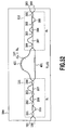
- FIG. 28 shows an optical multi/demultiplexing circuit which represents a sixth embodiment.
- This circuit is an N-stage lattice-form filter constituted by N+1 (N: an integer equal to or larger than 1) phase generating optical couplers 111 to 115, N optical delay lines 107 to 109 each interposed between one of adjacent pairs of the phase-generating optical couplers, two input waveguides 101 and 102 connected to the first phase generating optical coupler 111, and two output waveguides 103 and 104 connected to the (N+1)-th phase generating optical coupler 115.
- N+1 an integer equal to or larger than 1
- phase generating optical couplers 111 to 115 N optical delay lines 107 to 109 each interposed between one of adjacent pairs of the phase-generating optical couplers
- two input waveguides 101 and 102 connected to the first phase generating optical coupler 111
- two output waveguides 103 and 104 connected to the (N+1)-th phase generating optical coupler 115.
- Each of the N optical delay lines 107, 108, and 109 is formed by two optical delay elements.
- the path length differences of the optical delay lines 107, 108, and 109 are set at ⁇ L 1 + ⁇ L 1 , ⁇ L 2 + ⁇ L 2 , ..., ⁇ L N + ⁇ L N .
- a phase generating optical coupler in which its output phase difference has a wavelength dependence with respect to a passband is used as each of the phase generating optical couplers are used as a phase generating device to apply phases ⁇ 1 ( ⁇ ) , ⁇ 2 ( ⁇ ), ⁇ , ⁇ N ( ⁇ ) each having a wavelength dependence to the optical delay lines 107, 108, and 109. It is possible to freely set the optical characteristics of the optical multi/demultiplexing circuit shown in FIG. 28 by suitably setting these phases ⁇ 1 ( ⁇ ), ⁇ 2 ( ⁇ ) , ⁇ , ⁇ N ( ⁇ ).
- a designing method with which the transmittance spectra of a conventional optical multi/demultiplexing circuit with a uniform frequency period can be transformed into an optical multi/demultiplexing circuit with a uniform wavelength period will be described as a method used in this embodiment.
- an interferometer which is uniformly periodic with respect to frequency in theory can be changed into an interferometer uniformly periodic with respect to wavelength by using the method described in the first embodiment and so on.
- a different design method is used in this embodiment.
- optical multi/demultiplexing circuit e.g., an N-order (N: an integer equal to or larger than 1) optical multi/demultiplexing circuit (optical delay line circuit), which consists of optical delay lines and optical couplers
- N an integer equal to or larger than 1
- optical multi/demultiplexing circuit optical delay line circuit
- w the relative optical angular frequency
- ⁇ L the optical path length difference of the optical delay line, which includes a wavelength dependence of the refractive index
- c is the speed of light.
- the phase can be approximated by a quadratic or higher-degree polynomial function: ⁇ ⁇ ⁇ ⁇ L + ⁇ L ⁇ c - m + - ( ⁇ L + ⁇ L ) ⁇ c 2 + 1 ⁇ ⁇ ⁇ ⁇ - ⁇ c + ⁇ q ⁇ 2 ( - 1 ⁇ ) q ( ⁇ L + ⁇ L ) ( ⁇ - ⁇ c ⁇ ) q ⁇ c q + 1
- the phase shown by the equation (11) is applied to the optical delay line, thus realizing a uniform-wavelength-period optical multi/demultiplexing circuit having the center wavelength ⁇ c and the wavelength period ⁇ .
- phase generating optical coupler is used as a phase generating device.
- phase generating optical coupler Such a wavelength-dependent optical multi/demultiplexing devices capable of generating a wavelength dependent phase will be referred to as "phase generating optical coupler”.
- phase generating optical coupler an interferometer-type phase generating optical coupler constituted by an optical coupler and an optical delay line may be used. More specifically, a lattice-form filter type phase generating optical coupler constituted by M+1 (M: an integer equal to or larger than 1) optical couplers and M optical delay lines each interposed between adjacent pairs of the optical couplers is used as each phase generating optical coupler in this embodiment.
- phase generating optical coupler of this construction resides in that the lattice-form filter theoretically has no loss, and that it is possible to make an optical coupler of this construction function as a phase generating optical coupler by suitably setting the M+1 power coupling ratios (amplitude coupling ratios) of the optical couplers and the M optical path length differences of the optical delay lines. Also, a directional coupler formed of two optical waveguides placed close to each other can be used as each optical coupler.
- H n (z) and F n (z) are the through port and cross port transfer functions, respectively, of the n-th lattice-form-filter-type phase generating optical coupler
- M n is the number of optical delay lines of the n-th lattice-form-filter-type phase generating optical coupler
- z is a complex variable replaced for exp(j2 ⁇ 1/ ⁇ )
- H n* (z) is a para-Hermitian conjugate of H n (z) defined by H n * z ⁇ H n * 1 z * with the super
- a Mach-Zehnder interferometer which is an example of the optical multi/demultiplexing circuit.
- the optical delay line 107 is formed of two optical delay elements.
- the path length difference of the optical delay line 107 is set to ⁇ L 1 + ⁇ L 1 .
- the phase generating optical couplers 111 and 112 are M 1 -stage and M 2 -stage lattice-form-filter-type phase generating optical couplers respectively having transfer matrices S 1 and S 2 .
- one of the two optical couplers may be formed as a phase generating optical coupler or both of the two optical couplers may be formed as a phase generating optical coupler.
- ⁇ L a variable ⁇ L was introduced into the phase function for approximation, as shown in equation (11).
- the variable is not indispensable to the design of the phase generating optical coupler, and a variable other than this may be used.
- phase difference between the outputs of the phase generating optical coupler i.e., the generated phase ⁇ ( ⁇ ) coincided with the target phase ⁇ ( ⁇ ): ⁇ ⁇ ⁇ 0.55 - 0.84 ⁇ ⁇ - ⁇ c + 17 ( ⁇ - ⁇ c ⁇ ) 2 - 11 ( ⁇ - ⁇ c ⁇ ) 3
- the phase generating optical coupler functions as a 3-dB optical coupler having an amplitude coupling ratio of approximately 0.5.
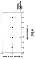
- FIG. 31 is a diagram schematically showing a fabricated uniform-wavelength-period Mach-Zehnder interferometer.
- ⁇ L 1 is the optical path length difference of the optical delay line of the conventional Mach-Zehnder interferometer.
- the above-described optical multi/demultiplexing circuit was fabricated by forming silica-based waveguides on a silicon substrate 504 by flame hydrolysis deposition, photolithography, and reactive ion etching. After the formation of the optical waveguides, thin film heaters having a width of 40 ⁇ m and a heater length of 4 mm were formed as a path length difference adjusting device 401 on the optical waveguides, and the refractive indices of the waveguides were changed by using the thin film heaters to correct fabrication errors of the optical path length differences of optical delay lines.
- the waveguides were made so as to have a relative refractive index difference of 1.5%, a core thickness of 4.5 ⁇ m and a core width of 4.5 ⁇ m.
- the chip on which this Mach-Zehnder interferometer was fabricated was cut out by dicing, and an optical module was assembled by connecting single-mode fibers to the input and output waveguides.
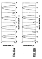
- FIG. 32 shows the optical characteristics of the fabricated uniform-wavelength-period Mach-Zehnder interferometer optical module.
- the characteristic relating to light which is input through the input waveguide 102 and output through the output waveguide 103 is indicated as "CROSS"
- the characteristic relating to light which is input through the input waveguide 102 and output through the output waveguide 104 is indicated as "THROUGH”.
- the optical multi/demultiplexing circuit having a uniform wavelength period of 40 nm was realized by using the principle of the present invention.
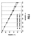
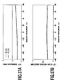
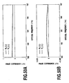
- FIG. 33 shows the misalignment of the center point of the passbands of the Mach-Zehnder interferometer from the CWDM grid with respect to the relative wavelength.
- FIG. 34 shows the loss with respect to the relative wavelength
- FIG. 35 shows the crosstalk with respect to the relative wavelength.
- the loss is increased on the CWDM grid and the crosstalk characteristic is also deteriorated since the center point of the passband deviates from the wavelength grid.
- the characteristics in terms of loss and crosstalk are good since the center point of the passband just coincides with the wavelength grid.
- a uniform-wavelength-period optical multi/demultiplexing circuit was realized in such a manner that in an interferometer-type optical circuit constituted by a phase generating optical coupler having at least one input and at least two outputs and an optical delay line coupled to the phase generating optical coupler, a phase designed to obtain a uniform-wavelength-period characteristic was applied to the optical delay line by a phase generating device.
- phase generating optical coupler characterized in that the output phase difference varies with respect to a passband was used as the phase generating device. More concretely, a lattice-form filter type phase generating optical coupler was used as the phase generating optical coupler, and the parameters for designing the phase generating optical coupler were optimized so that the optical coupler had the desired phase and amplitude coupling ratio, thus achieving success in enabling the phase generating optical coupler to function as desired.
- a conventional Mach-Zehnder interferometer was transformed into a uniform-wavelength-period Mach-Zehnder interferometer as an example of an optical multi/demultiplexing circuit. This means that ordinary optical delay line circuits uniformly periodic with respect to frequency can be transformed to become uniformly periodic with respect to wavelength.
- a uniform-wavelength multi/demultiplexing circuit can also be realized by a different method, e.g., a method such as those described in the first embodiment where the target phase was derived directly from the transmittance spectra, to obtain the desired optical characteristics.
- the target phase function is not limited to the one described in this embodiment, and other phase functions can be used to obtain the desired characteristics.
- the present invention is not limited to converting the transmittance characteristics into uniform wavelength period.
- the phase may be designed such that the wavelength periods are different at different wavelength regions. Transforming the transmittance spectra of the conventional optical multi/demultiplexing circuit into equal wavelength spacing is only an example of the phase design.
- the way in which a phase is expressed is not uniquely determined.
- a plurality of ways of expression are possible for realization of the same characteristic.
- m can be set at m' /2 (m' : an integer). Any other functions may be used.
- This embodiment is only an example of a possible use of a phase generating device to modify the optical characteristics of the conventional optical multi/demultiplexing circuits.
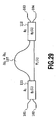
- FIG. 36 shows an optical multi/demultiplexing circuit in a seventh embodiment
- Each of the two optical delay lines 107 and 108 is formed by two optical delay elements.
- the path length differences of the optical delay lines 107 and 108 are respectively set at ⁇ L 1 + ⁇ L 1 and ⁇ L 2 + ⁇ L 2 .
- a phase generating optical coupler in which its output phase difference has a wavelength dependence with respect to a passband is used as each of the phase generating optical couplers 111 to 113 .
- These phase generating optical couplers are used as a phase generating device to apply phases ⁇ 1 ( ⁇ ) and ⁇ 2 ( ⁇ ), each having a wavelength dependence, to the optical delay lines 107 and 108. It is possible to freely set the optical characteristics of the optical multi/demultiplexing circuit shown in FIG. 36 by suitably setting these phases ⁇ 1 ( ⁇ ) and ⁇ 2 ( ⁇ ).
- a wavelength reference device in which its transmittance spectrum is transformed from uniform frequency period into uniform wavelength period, will be described by way of example. If the phase described in the description of the sixth embodiment is applied to the optical delay line, a wavelength reference device having a center wavelength ⁇ c and a wavelength period ⁇ can be realized. In this embodiment, phase generating optical couplers are used as a phase generating device to achieve the desired optical characteristics.
- phase generating optical couplers of a lattice-form filter type are used, the phase ⁇ 1 ( ⁇ ) is applied to the optical delay line 107 by the phase generating optical couplers 111 and 112, and the phase ⁇ 2 ( ⁇ ) is applied to the optical delay line 108 by the phase generating optical couplers 112 and 113.
- the fundamental optical path length difference ⁇ L is equal to the path length difference of a conventional wavelength reference device of a lattice-form filter type.
- the phase generating optical coupler 112 was formed by a directional coupler formed of two optical waveguides placed close to each other, and the phase generating optical couplers 111 and 113 were formed by M 1 -stage and M 3 -stage lattice-form-filter-type phase generating optical couplers respectively having transfer matrices S 1 and S 3 .
- the entire circuit was designed so as to be line-symmetric about the phase generating optical coupler 112. The number of circuit parameters was reduced to facilitate the fabrication of the circuit.
- the above-described configuration is only an example of the circuit configuration, and any other circuit configuration, e.g., one in which the characteristics of the phase generating optical couplers 111 and 113 differ from each other may be used.
- the design parameters of the phase generating optical couplers were optimized so that the phases ⁇ 1 ( ⁇ ) and ⁇ 2 ( ⁇ ) applied to the optical delay lines 107 and 108 and the target phases ⁇ 1 ( ⁇ ) and ⁇ 2 ( ⁇ ) respectively coincided with each other, and so that the phase generating optical couplers
- the entire circuit is made line-symmetric about the phase generating optical coupler 112 and the designs of the optical delay lines 107 and 108 are identical with each other. Therefore, only the optimization for the optical delay line 107 is necessary. As a result of the optimization, the corresponding phase generating optical coupler was formed as a six-stage lattice-form filter. If the number of parameters was smaller, the phase generating optical coupler will become easier to fabricate.
- restrictive conditions are not necessary for derivation of parameters for the design of the phase generating optical coupler, and other restrictive conditions may be set. If the number of stages in the lattice-form-filter-type phase generating optical coupler is increased, the degree of approximation to the desired characteristics can be increased. The degree of approximation is also increased by using arbitrary design parameters without imposing restrictive conditions.
- variable ⁇ L 1 was introduced into the phase function for approximation.
- the variable is not indispensable to design the phase generating optical coupler, and a variable other than this may be used.
- the amplitude coupling ratios of the optical couplers constituting the phase generating optical coupler, the optical path length differences of the optical delay lines constituting the phase generating optical coupler and the variable ⁇ L 1 were optimized by the conjugate gradient method so that the generated phase difference ⁇ 1 ( ⁇ ) and the target phase ⁇ 1 ( ⁇ ) coincided with each other and the amplitude coupling ratio was 0.3.
- the phase difference ⁇ 1 ( ⁇ ) shown in FIG. 37A was produced by the phase generating optical couplers 111 and 112 and the phase ⁇ 1 ( ⁇ ) was suitably approximated.
- a phase generating optical coupler (phase generating optical coupler 111) having this phase difference and the amplitude coupling ratio shown in FIG. 37B was realized.
- FIG. 38 is a diagram schematically showing a fabricated uniform-wavelength-period lattice-form-filter-type wavelength reference device.
- ⁇ L is the optical path length difference of the optical delay lines of the conventional lattice-form filter.
- the amplitude coupling ratio of a directional coupler 310 was set at 0.4.
- the above-described optical multi/demultiplexing circuit was fabricated by forming silica-based optical waveguides on a silicon substrate 504 by flame hydrolysis deposition, photolithography or reactive ion etching. After the formation of the optical waveguides, thin film heaters having a width of 70 ⁇ m and a heater length of 8 mm were formed as a path length difference adjusting device 401 on the optical waveguides, and the refractive indices of the waveguides were changed by using the thin filmheaters to correct fabrication errors of the optical path length differences of the optical delay lines.
- the waveguides were made so as to have a relative refractive index difference of 1.5%, a core thickness of 4.5 ⁇ m and a core width of 4.5 ⁇ m.
- the chip on which this Mach-Zehnder interferometerwas fabricated was cut out by dicing, and an optical module was assembled by connecting dispersion-shifted fibers to the input and output waveguides.
- FIG. 39A shows the transmission characteristics of the conventional wavelength reference device
- FIG. 39B shows the transmission characteristics of the wavelength reference device. These optical characteristics were measured when light was input through the input waveguide 102 and output through the output waveguide 103.
- the conventional lattice-form filter cannot be made uniformly periodic on the wavelength axis since it is uniformly periodic with respect to frequency.
- the wavelength reference device having a uniform wavelength period of 40 nm was realized by using the principle of the present invention.
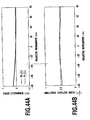
- FIG. 40 shows the deviation of the center point of the passband of the lattice-form filter from the CWDM grid with respect to the relative wavelength. It can be understood that a large axial deviation occurs in the conventional lattice-form filter since the conventional lattice-form filter is uniformly periodic with respect to frequency and not uniformly periodic with respect to wavelength. In contrast, no axial deviation occurs in the uniform-wavelength-period lattice-form filter of the present invention since the lattice-form filter of the present invention has a uniform wavelength period of 40 nm. Therefore, the lattice-form filter of the present invention is suitable for use as a wavelength reference device for the CWDM system using a grid periodic in a wavelength region.
- FIG. 41 shows the loss with respect to the relative wavelength.
- the loss is increased on the CWDM grid and the crosstalk characteristic is also deteriorated since the center point of the passband deviates from the wavelength grid.
- the present lattice-form filter no loss due to axial deviation occurs since the center point of the passband just coincides with the wavelength grid.
- a uniform-wavelength-period optical multi/demultiplexing circuit was realized in such a manner that in an interferometer-type optical circuit constituted by a phase generating optical coupler having at least one input and at least two outputs and an optical delay line coupled to the phase generating optical coupler, a phase designed to obtain a uniform-wavelength-period characteristic was applied to the optical delay line by a phase generating device.
- phase generating optical coupler characterized in that the output phase difference varies with respect to a passband was used as the phase generating device. More concretely, a lattice-form filter type phase generating optical coupler was used as the phase generating optical coupler, and the parameters for designing the phase generating optical coupler were optimized so that the optical coupler had the desired phase and amplitude coupling ratio, thus achieving success in enabling the phase generating optical coupler to function as desired.
- a conventional lattice-form-filter-type wavelength reference device was transformed into a uniform-wavelength-period lattice-form-filter-type wavelength reference device as an example of an optical multi/demultiplexing circuit.
- a suitable phase function may be set as desired according to the transmission characteristics to be obtained.
- the present invention is not limited to the uniform-wavelength-period wavelength reference device.
- the phase may be designed such that the wavelength periods are different at different wavelength regions. Therefore, a wavelength reference device having a peak of transmissivity, i.e., a wavelength reference point, set at an arbitrary position can be realized by suitably setting the phase.
- This embodiment is only an example of a possible use of a phase generating device to modify the optical characteristics of the conventional optical multi/demultiplexing circuits.
- FIG. 42 shows an optical multi/demultiplexing circuit in an eighth embodiment.
- Each of the two optical delay lines 107 and 108 is formed by two optical delay elements.
- the path length differences of the optical delay lines 107 and 108 are respectively set to ⁇ L 1 + ⁇ L 1 and ⁇ L 2 + ⁇ L 2 .
- a phase generating optical coupler in which its output phase difference has a wavelength dependence with respect to a passband is used as each of the phase generating optical couplers 111 to 113 .
- These phase generating optical couplers are used as a phase generating device to apply phases ⁇ 1 ( ⁇ ) and ⁇ 2 ( ⁇ ) each having a wavelength dependence to the optical delay lines 107 and 108. It is possible to freely set the optical characteristics of the optical multi/demultiplexing circuit shown in FIG. 42 by suitably setting these phases ⁇ 1 ( ⁇ ) and ⁇ 2 ( ⁇ ).
- phase generating optical couplers are used as a phase generating device to achieve the desired optical characteristics.
- phase generating optical couplers of a lattice-form filter type are used, the phase ⁇ 1 ( ⁇ ) is applied to the optical delay line 107 by the phase generating optical couplers 111 and 112, and the phase ⁇ 2 ( ⁇ ) is applied to the optical delay line 108 by the phase generating optical couplers 112 and 113.
- the fundamental optical path length difference ⁇ L is equal to the path length difference of a conventional interleave filter of a lattice-form filter type.
- the phase generating optical coupler 112 was formed by a directional coupler 310 formed of two optical waveguides placed close to each other and having an amplitude coupling ratio of 0.38.
- the phase generating optical couplers 111 and 113 were formed by M 1 -stage and M 3 -stage lattice-form-filter-type phase generating optical couplers respectively having transfer matrices S 1 and S 3 .
- phase generating optical couplers were optimized so that the phases ⁇ 1 ( ⁇ ) and ⁇ 2 ( ⁇ ) applied to the optical delay lines 107 and 108 and the target phases ⁇ 1 ( ⁇ ) and ⁇ 2 ( ⁇ ) respectively coincided with each other, and so that the phase generating optical couplers 111 and 113 functions as optical couplers having amplitude coupling ratios of 0.5 and 0.15, respectively, as described above in the description of the sixth embodiment.
- the phase generating optical couplers 111 and 113 were formed as a six-stage lattice-form filter and a ten-stage lattice-form filter, respectively, as shown in FIGS. 43A and 43C.
- restrictive conditions are not necessary for derivation of parameters for the design of the phase generating optical couplers, and other restrictive conditions may be set. If the number of stages in each lattice-form-filter-type phase generating optical coupler is increased, the degree of approximation to the desired characteristics can be increased. The degree of approximation is also increased by using arbitrary design parameters without imposing restrictive conditions. However, even when the above-described restrictive conditions were imposed, the design parameters were derived with a sufficiently high degree of approximation by optimization.
- variables ⁇ L 1 and ⁇ L 2 were respectively introduced into the phase functions ⁇ 1 ( ⁇ ) and ⁇ 2 ( ⁇ ) for approximation.
- the variables are not indispensable to design the phase generating optical couplers, and other variables may be used.
- the amplitude coupling ratios of the optical couplers constituting the phase generating optical coupler, the optical path length differences of the optical delay lines constituting the phase generating optical coupler and the variable ⁇ L 1 were optimized by the conjugate gradient method so that the generated phase difference ⁇ 1 ( ⁇ ) and the target phase ⁇ 1 ( ⁇ ) coincided with each other and the amplitude coupling ratio was 0.5.
- the phase difference ⁇ 1 ( ⁇ ) shown in FIG. 44A was produced by the phase generating optical couplers 111 and 112 and the phase ⁇ 1 ( ⁇ ) was suitably approximated.
- a phase generating optical coupler (phase generating optical coupler 111) having this phase difference and the amplitude coupling ratio shown in FIG. 44B was realized.
- the amplitude coupling ratios of the optical couplers constituting the phase generating optical coupler, the optical path length differences of the optical delay lines constituting the phase generating optical coupler and the variable ⁇ L 2 were optimized by the conjugate gradient method so that the generated phase difference ⁇ 2 ( ⁇ ) and the target phase ⁇ 2 ( ⁇ ) coincided with each other and the amplitude coupling ratio was 0.15.
- phase difference ⁇ 2 ( ⁇ ) shown in FIG. 45A was produced by the phase generating optical couplers 112 and 113 and the phase ⁇ 2 ( ⁇ ) was suitably approximated.
- the phase generating optical coupler (phase generating optical coupler 113) having this phase difference and the amplitude coupling ratio shown in FIG. 45B was realized.
- ⁇ L is the optical path length difference of the optical delay lines of the conventional lattice-form filter.
- the amplitude coupling ratio of a directional coupler 310 was set at 0.38.
- the above-described optical multi/demultiplexing circuit was fabricated by forming silica-based optical waveguides on a silicon substrate 504 by flame hydrolysis deposition, photolithography or reactive ion etching. After the formation of the optical waveguides, thin film heaters having a width of 40 ⁇ m and a heater length of 5 mm were formed as a path length difference adjusting device 401 on the optical waveguides, and the refractive indices of the waveguides were changed by using the thin film heaters to correct fabrication errors of the optical path length differences of the optical delay lines.
- the waveguides were made so as to have a relative refractive index difference of 1.5%, a core thickness of 4.5 ⁇ m and a core width of 4.5 ⁇ m.
- the chip on which this Mach-Zehnder interferometer was fabricated was cut out by dicing, and an optical module was assembled by connecting single-mode fibers to the input and output waveguides.
- FIG. 46 shows the transmission characteristics of the lattice-type interleave filter of the present invention.
- the characteristic relating to light which is input through the input waveguide 102 and output through the output waveguide 103 is indicated as "CROSS"
- the characteristic relating to light which is input through the input waveguide 102 and output through the output waveguide 104 is indicated as "THROUGH”.
- the interleave filter of the present invention is most suitable for use as an optical multi/demultiplexing circuit for the CWDM system.
- a uniform-wavelength-period optical multi/demultiplexing circuit was realized in such a manner that in an interferometer-type optical circuit constituted by a phase generating optical coupler having at least one input and at least two outputs and an optical delay line coupled to the phase generating optical coupler, a phase designed to obtain a uniform-wavelength-period characteristic was applied to the optical delay line by a phase generating device.
- phase generating optical coupler characterized in that the output phase difference varies with respect to a passband was used as the phase generating device. More concretely, a lattice-form filter type phase generating optical coupler was used as the phase generating optical coupler, and the parameters for designing the phase generating optical coupler were optimized so that the optical coupler had the desired phase and amplitude coupling ratio, thus achieving success in enabling the phase generating optical coupler to function as desired.
- a conventional lattice-form-filter-type interleave filter was transformed into a uniform-wavelength-period lattice-form-filter-type interleave filter as an example of an optical multi/demultiplexing circuit.
- the optical multi/demultiplexing circuit usable in a single state, may be used in a state of being connected to another optical circuit such as arrayed waveguide gratings, or in a state of being integrated with another optical circuit such as arrayed waveguide gratings on one chip so as to form an optical multi/demultiplexing module, as described above in the description of the fourth embodiment of the present invention.
- the uniform-wavelength-period optical multi/demultiplexing circuit of the present invention may be combined with a conventional optical circuit in this manner.
- An arrayed waveguide grating i.e., an interferometer constituted by an optical multi/demultiplexing device (slab waveguide) and an optical delay line (array waveguide), is an optical circuit which operates on a principle different from the principle on which the optical delay line circuit used in each embodiment of the present invention operates. Therefore, the optical characteristics of the arrayed waveguide grating differ from those of the optical delay line circuit of the present invention. Ordinarily, the optical characteristics of the arrayed waveguide are uniformly periodic with respect to wavelength period. It is known that the arrayed waveguide grating can be made uniformly periodic with respect to frequency by using a method different from that in the present invention.
- the circuit is designed so that the center wavelength of an optical multi/demultiplexing circuit 801 in a front stage and the center wavelength of optical multi/demultiplexing circuits 802 and 803 in a rear stage differ by the half-wavelength value.
- other input and output ports may be used and there are a number of methods for cascading.
- Optical multi/demultiplexing circuits in accordance with the present invention may be cascaded in any configuration.
- any P-input Q-output multi/demultiplexing circuit may be formed.
- This embodiment is only an example of a possible use of a phase generating device to modify the optical characteristics of the conventional optical multi/demultiplexing circuits.
- a conventional optical delay line circuit is uniformly periodic in an optical frequency region, and its transmission characteristics are characterized by an optical frequency period ⁇ f and a center optical frequency fc.
- the optical frequency period ⁇ f and the center optical frequency fc cannot be set simultaneously; only one of them can be set.
- Equations (23) and (24) are substituted in equation (22) to obtain the following equations for the transmission characteristics:
- nc is the refractive index at the center optical frequency
- Ngc is the group refractive index at the center optical frequency.
- the optical frequency period can be set to an arbitrary value and an optical multi/demultiplexing circuit uniformly periodic with respect to frequency and having the optical frequency period ⁇ f can be formed.
- the center optical frequency cannot be set.
- the center optical frequency can be set to an arbitrary value and an optical multi/demultiplexing circuit uniformly periodic with respect to frequency and having the center optical frequency fc can be formed.
- the optical frequency period cannot be set.
- FIGS. 48A and 48B shows a concrete example of the deviation from an optical frequency grid of the center point of the passbands in the transmission characteristics of a conventional Mach-Zehnder interferometer having an optical frequency period of 800 GHz.
- the optical frequency grid is assumed to have a center optical frequency of 191 THz and an optical frequency period of 800 GHz.
- FIG. 48A shows the amount of axial deviation in the case of designing using equation (25), and FIG. 48B shows the amount of axial deviation in the case of designing using equation (26).
- the amount of axial deviation is constant with respect to the optical frequency since the optical frequency period is set at 800 GHz , but the amount of axial deviation from the optical frequency grid is large since the center optical frequency cannot be set.
- the amount of deviation from the optical frequency grid is zero at the center of the frequency region since the center optical frequency is set at 191 THz, but the amount of axial deviation from the optical frequency grid is large at both ends of the frequency region.
- the conventional optical delay line circuit is ordinarily capable of setting either the optical frequency period ⁇ f or the center optical frequency fc, but incapable of simultaneously setting both of them at arbitrary values.
- f c m s N gc ⁇ f/n c (ms : an integer) is satisfied
- both the optical frequency period ⁇ f and the center optical frequency fc can be set simultaneously.
- both the optical frequency period ⁇ f and the center optical frequency fc can be set only in such a special case.
- a phase generating device having an optical frequency dependence is applied to enable both the optical frequency period ⁇ f and the center optical frequency fc to be set simultaneously at arbitrary values, as described below.
- the transmission characteristics of the optical multi/demultiplexing circuit can be freely changed by suitably setting the phase ⁇ (f) having an optical frequency dependence.
- a uniform-frequency-period optical delay line circuit having a transmission spectrum with optical frequency period ⁇ f and center optical frequency fc, for example, is to be obtained. Therefore, the nonlinear phase ⁇ (f) shown by the following equation may be applied to the optical delay line of the optical delay line circuit.
- ⁇ f n ( ⁇ L + ⁇ L ) c - 1 ⁇ f ⁇ f - m c - f c ⁇ f
- ⁇ L is the path length difference of the conventional Mach-Zehnder interferometer
- mc is an integer.
- a phase generating optical coupler is used as a phase generating device to generate an optical-frequency-dependent phase, whereby the desired optical characteristics are realized.
- FIGS. 49 shows a concrete example of the deviation from an optical frequency grid of the center point of the passband in the transmission characteristics of the Mach-Zehnder interferometer having an optical frequency period of 800 GHz when the phase expressed by equation (28) is applied to the optical delay line of the Mach-Zehnder interferometer. It can be understood that since the center optical frequency is set at 191 THz and the optical frequency period is set at 800 GHz, the center point just coincides with the optical frequency grid so the axial deviation from the optical frequency grid is eliminated.
- An interferometer type phase generating optical coupler constituted by optical couplers and optical delay lines was used. More specifically, in this embodiment, a lattice-form filter type optical multi/demultiplexing device constituted by M+1 (M: an integer equal to or larger than 1) optical couplers and M optical delay lines each interposed between adjacent pairs of the optical couplers.
- the advantage of using an optical multi/demultiplexing device of this construction as a phase generating device resides in that the lattice-form filter theoretically has no loss, and that it is possible to make the optical multi/demultiplexing device function as a phase generating optical coupler by suitably setting the power coupling ratios (amplitude coupling ratios) of the M+1 optical couplers and the optical path length differences of the M optical delay lines. Also, a directional coupler formed of two optical waveguides placed close to each other is used as each optical coupler.
- the transfer matrix of the n-th two-input two-output lattice-form-filter-type phase generating optical coupler of the optical multi/demultiplexing circuit can be written as equation (12) shown above in the description of the sixth embodiment.
- z is a complex variable replaced for exp(j ⁇ ⁇ l/c).
- ⁇ n,p is the amplitude coupling ratio of the p-th optical coupler in the n-th lattice-form-filter-type phase generating optical coupler, more specifically the angular expression
- one of the two optical couplers may be formed as a phase generating optical coupler or both of the two optical couplers may be formed as a phase generating optical coupler.
- two phase generating optical couplers identical with each other were used and were placed so as to be line-symmetric about the middle point of the optical delay line of the Mach-Zehnder interferometer, as described above in the description of the first embodiment.
- phase generating optical couplers are placed so as to be line-symmetric about the center of the optical delay line of the Mach-Zehnder interferometer.
- this restrictive condition is not necessary for derivation of parameters for the design of the phase generating optical coupler, and other restrictive conditions may be set.
- the two phase generating optical couplers of the Mach-Zehnder interferometer may be designed differently from each other, and only one of them may be designed to function as a phase generating device. While a three-stage lattice-form filter was used as a phase generating optical coupler having a phase generating function in this embodiment, a two-stage lattice-form filter, a lattice-form filter having four or more stages or one-stage lattice-form filter, i.e., a Mach-Zehnder interferometer, may alternatively be used. Needless to say, any other optical multi/demultiplexing device may be made to function as the phase generating optical coupler.
- a variable may be introduced into the target phase function to facilitate the approximation because there will be a larger flexibility in the design parameters of the phase generating optical coupler. Therefore, a variable ⁇ L 1 was introduced into the phase function for approximation. Needless to say, the variable is not indispensable to design the phase generating optical coupler, and a variable other than this may be used.
- the amplitude coupling ratios of the optical couplers constituting the phase generating optical coupler, the optical path length differences of the optical delay lines constituting the phase generating optical coupler and the variable ⁇ L 1 were optimized by the conjugate gradient method so that the generatedphase difference ⁇ 1 ( ⁇ ) and the target phase ⁇ 1 ( ⁇ ) coincided with each other and the amplitude coupling ratio was 0.5.
- phase difference ⁇ 1 ( ⁇ ) shown in FIG. 50A was produced by the phase generating optical couplers 111 and 112 and the phase ⁇ 1 ( ⁇ ) was suitably approximated.
- Fig.50B shows the non-linear term of the phase extracted from Fig. 50A. A good correspondence between the target phase and the phase created by the phase generating optical coupler can be recognized.
- phase generating optical couplers were capable of functioning as an optical coupler having an amplitude coupling ratio of 0.5, as shown in FIG. 51.
- FIG. 52 is a diagram schematically showing the fabricated Mach-Zehnder interferometer.
- ⁇ L 1 is the path length difference of the optical delay line of the conventional Mach-Zehnder interferometer.
- the above-described optical multi/demultiplexing circuit was fabricated by forming silica-based optical waveguides on a silicon substrate 504 by flame hydrolysis deposition, photolithography, and reactive ion etching. After the formation of the optical waveguides, thin film heaters having a width of 70 ⁇ m and a heater length of 2 mm were formed as a path length difference adjusting device 401 on the optical waveguides, and the refractive indices of the waveguides were changed by using the thin filmheaters to correct fabrication errors of the optical path length differences of the optical delay lines.
- the waveguides were made so as to have a relative refractive index difference of 0.75%, a core thickness of 7 ⁇ m and a core width of 7 ⁇ m.
- the chip on which this Mach-Zehnder interferometer was fabricated was cut out by dicing, and an optical module was assembled by connecting single-mode fibers to the input and output waveguides.
- FIG. 53 shows the optical characteristics of the fabricated Mach-Zehnder interferometer module.
- the characteristic relating to light which is input through the input waveguide 102 and output through the output waveguide 103 is indicated as "CROSS", while the characteristic relating to light which is input through the input waveguide 102 and output through the output waveguide 104 is indicated as "THROUGH”.
- the optical multi/demultiplexing circuit having an optical frequency period of 800 GHz and a center optical frequency of 191 THz was realized by using the above described principle. Needless to say, the optical frequency period and the center frequency may be set at 100 GHz and 191 THz, respectively, for adaptation to the ITU grid.
- FIG. 54 shows the deviation of the center point of the passbands of the Mach-Zehnder interferometer from an optical frequency grid (having an optical frequency period of 800 GHz and a center optical frequency of 191 THz) with respect to the optical frequency. No axial deviation occurred in the Mach-Zehnder interferometer, and the characteristics shown in FIG. 49 were realized, as expected from the theory.
- an optical multi/demultiplexing circuit capable of simultaneously setting the optical frequency period and the center optical frequency to arbitrary values was realized in such a manner that in an interferometer-type optical circuit constituted by a phase generating optical coupler having at least one input and at least two outputs and an optical delay line coupled to the phase generating optical coupler, an optical-frequency-dependent phase was applied to the optical delay line by a phase generating device.
- phase generating optical coupler characterized in that the output phase difference varies with respect to a passband (having an optical frequency dependence) was used as the phase generating device. More concretely, a lattice-form filter type phase generating optical coupler was used as the phase generating optical coupler, and the parameters for designing the phase generating optical coupler were optimized so that the optical coupler had the desired phase and amplitude coupling ratio, thus achieving success in enabling the phase generating optical coupler to function as desired.
- the above described principle is useful not only in the wavelength region but also in the optical frequency region.
- the above-described series of design algorithms for the process of deriving the phase for realization of the desired characteristics and optimizing the parameters for designing the phase generating optical coupler by numerical analysis is one possible method for implementation of the present invention, and any other method, e.g., a method such as those described in the first embodiment where the target phase was derived directly from the transmittance spectra, may be used.
- the target phase function is not limited to the one described in this embodiment, and other phase functions can be used to obtain the desired characteristics.
- the present invention is not limited to optical multi/demultiplexing circuit capable of setting the optical frequency period and the center optical frequency simultaneously at arbitrary values.
- the phase may be designed such that the frequency periods are different at different frequency regions.
- FIG. 55 shows the deviation from an optical frequency grid of the center point of the passband in the transmission characteristics of a Mach-Zehnder interferometer having an optical frequency period of 800 GHz when the phase set as described above is applied to the optical delay line of the Mach-Zehnder interferometer.
- the center optical frequency and the optical frequency period of the optical frequency grid are set at 190.8 THz and 800 GHz, respectively.
- This embodiment is only an example of a possible use of a phase generating device to modify the optical characteristics of the conventional optical multi/demultiplexing circuits.
- a lattice-form filter type optical multi/demultiplexing device constituted by M+1 (M: an integer equal to or larger than 1) optical couplers and M optical delay lines each interposed between adjacent pairs of the optical couplers was mainly used as a phase generating device.
- M an integer equal to or larger than 1
- the lattice-form filter theoretically has no loss, and because it is possible to make lattice-form filter type optical multi/demultiplexing device function as a phase generating optical coupler by suitably setting the power coupling ratios (amplitude coupling ratios) of the M+1 optical couplers and the optical path length differences of the M optical delay lines.
- a directional coupler formed of two optical waveguides placed close to each other was used as the optical coupler because the amplitude coupling ratio of the directional coupler can be changed simply by adjusting the coupling length of the directional coupler.
- phase generating device formed by cascading lattice-form filters or any other interferometer-type optical multi/demultiplexing device constituted by an optical coupler and an optical delay line may be used as a phase generating device.
- This embodiment will be described with respect to the configuration, of other examples of phase generating devices.
- the above described principle can be applied regardless of the configuration of the phase generating device, and usable phase generating devices are not limited to the described configurations in the above embodiments.
- FIG. 56 shows a phase generating device in a tenth embodiment.
- This phase generating device is constituted by M+1 (M: an integer equal to or larger than 1) optical couplers 201 to 204, M optical delay lines 205 to 207 each interposed between adjacent pairs of the optical couplers 201 to 204, an input port connected to the first optical coupler 201, and an output port connected to the (M+1)-th optical coupler 204.
- M+1 an integer equal to or larger than 1
- any other kinds of coupler e.g., a multimode interference coupler, a variable coupler, an X-branch coupler and a Y-branch coupler may be used.
- An interferometer type optical coupler may also be used.
- a stabilized optical coupler capable of obtaining an amplitude coupling ratio with stability against manufacturing variation was used, as shown in FIG. 56.
- the stabilized optical coupler is a lattice-form circuit formed of four optical couplers (directional couplers) 211 to 214 and three optical delay lines 231 to 233), and the circuit of the stabilized optical coupler as a whole functions as a coupling element.
- the amplitude coupling ratio of each optical couplers (directional couplers) 211 to 214 is set at 0.5, and the optical path differences of the optical delay lines 231, 232, and 233 are set at ⁇ c/4, ⁇ , and - ⁇ c/4 ( ⁇ c: center wavelength), respectively.
- the amplitude coupling ratio of the stabilized coulter can be set by adjusting the value of ⁇ . If such an optical coupler is used as each optical couplers 201 to 204 constituting the phase generating optical coupler 111, the tolerance to manufacturing errors is increased.
- a phase generating optical coupler was realized by optimizing the amplitude coupling ratios of the optical couplers constituting the optical multi/demultiplexing device 111, i.e., the stabilized couplers 201 to 204, and the optical path length differences of the optical delay lines 205 to 207 constituting the optical multi/demultiplexing device 111.
- FIG. 57 shows a phase generating device in a first modification of the tenth embodiment.
- An optical multi/demultiplexing device 114 shown in FIG. 57 is constituted by a plurality of optical multi/demultiplexing devices 111, 112, and 113. More concretely, the optical multi/demultiplexing devices 112 and 113 are connected to two output ports of the optical multi/demultiplexing device 111 in a cascading manner.
- the optical multi/demultiplexing device 114 is a phase generating optical coupler.
- each of the optical multi/demultiplexing devices 111, 112, and 113 is a phase generating optical coupler.
- a plurality of optical multi/demultiplexing devices each functioning as a phase generating optical coupler may be used to form any P-input Q-output (P, Q : a natural number) phase generating optical coupler.
- the arrangement shown in FIG. 57 is a four-input four-output phase generating optical coupler.
- any ports may be used as an input port or an output port.
- light is input through one input port of the phase generating optical coupler and the amplitude coupling ratio and the phase difference of light output from two output ports are used for the function of the phase generating optical coupler.
- the numbers of input and output ports are freely selected as in this embodiment. For example, in a case where four output ports are provided, the amplitude coupling ratios and the relative phase differences of light output from the output ports can be defined.
- FIG. 58 shows an optical multi/demultiplexing circuit using the optical multi/demultiplexing device 114 shown in FIG. 57.
- the optical delay line 107 is formed of two optical delay elements and the optical path length difference thereof is set to ⁇ L 1 + ⁇ L 1 .
- a directional coupler provided as an optical coupler was used.
- a phase generating optical coupler whose output phase difference is wavelength dependent or optical frequency dependent with respect to a passband was used as the first phase generating optical coupler 114.
- This phase generating optical coupler is used as a phase generating device to apply a wavelength dependent or optical frequency dependent phase ⁇ 1 to the optical delay line 107.
- the optical characteristics of the optical multi/demultiplexing circuit as shown in FIG. 58 were set as desired by suitably setting this phase ⁇ 1 .
- FIG. 59 shows a phase generating device in a second modification of the tenth embodiment.
- a phase generating optical coupler 111 shown in FIG. 59 is constituted by optical couplers 201 to 204 and optical delay elements 251 to 255.
- the configuration of the phase generating optical coupler 111 may be called a transversal-form filter type optical multi/demultiplexing circuit in a broad sense.
- This optical multi/demultiplexing circuit is constituted by the optical coupler 201, an input port connected to the optical coupler 201, the optical delay element 251 connected to one of two output ports of the optical coupler 201, the optical delay element 254 connected to the other output port of the optical coupler 201, the optical coupler 202 connected to the optical delay element 254, the optical delay elements 252 and 253 connected to the optical coupler 202, the optical coupler 203 connected to the optical delay elements 252 and 253, the optical coupler 204 connected to the optical coupler 203 and the optical delay element 251, and an output port connected to the optical coupler 204.
- the amplitude coupling ratio of the optical couplers constituting the phase generating optical coupler 111 and the optical path length differences of the optical delay lines are suitably set to enable the phase generating optical coupler 111 to function as desired.
- An arrangement such as one shown in FIG. 60 may also be called a transversal-form filter type optical multi/demultiplexing circuit in a broad sense.
- This optical multi/demultiplexing circuit is constituted by an optical coupler 201, an input port connected to the optical coupler 201, an optical delay element 251 connected to one of two output ports of the optical coupler 201, an optical delay element 254 connected to the other output port of the optical coupler 201, an optical coupler 202 connected to the optical delay element 254, optical delay elements 252 and 253 connected to the optical coupler 202, an optical coupler 203 connected to the optical delay elements 252 and 253 and to the optical delay element 251, and three output ports connected to the optical coupler 203.
- the optical coupler 203 may be formed of a three-input three-output multiple mode interferometer or the like or may be formed of a plurality of optical couplers.
- the amplitude coupling ratio of the optical couplers constituting the phase generating optical coupler 111 and the optical path length differences of the optical delay lines are suitably set to enable the phase generating optical coupler 111 to function as desired.
- FIG. 61 shows an optical multi/demultiplexing circuit in an eleventh embodiment.
- This circuit is an N-stage lattice-form filter constituted by N+1 (N: an integer equal to or larger than 1) optical couplers 211 to 215, N optical delay lines 107 to 109 each interposed between adjacent pairs of the optical couplers, two input waveguides 101 and 102 connected to the first optical coupler 211, and two output waveguides 103 and 104 connected to the (N+1)-th optical coupler 215.
- Each of the N optical delay lines 107, 108, and 109 is formed of two optical delay elements, and the optical path length differences thereof are set at ⁇ L 1 + ⁇ L 1 , ⁇ L 2 + ⁇ L 2 , ..., ⁇ L N + ⁇ L N .
- Phases ⁇ 1 , ⁇ 2 , ⁇ , ⁇ N each having a wavelength dependence or an optical frequency dependence with respect to a pass band are applied to the optical delay lines 107, 108, and 109.
- the optical characteristics of the optical multi/demultiplexing circuit shown in FIG. 61 can be set as desired by suitably setting the above-mentioned phases shown above.
- phase generating devices are provided in the optical delay lines.
- FIG. 62 shows a state in which phase generating optical couplers 111 to 116 are provided in the pairs of optical delay elements forming the optical delay lines 107 to 109.
- a phase generating optical coupler formed by using optical couplers and optical delay lines can be used.
- FIG. 63 is a diagram schematically showing a Mach-Zehnder interferometer as a simple example of the optical multi/demultiplexing circuit in this embodiment.
- Thin film heaters provided as path length difference adjusting devices 401 for eliminating fabrication errors are formed in the optical delay line 107.
- the optical path length difference of the optical delay line 107 is adjusted to ⁇ L 1 + ⁇ L 1 by the two optical delay elements and the path length difference adjusting devices 401.
- phase generating optical coupler 111 As the phase generating optical coupler 111, a lattice-form phase generating device constituted by optical couplers 212 to 215 and optical delay lines 231 to 233 each interposed between adjacent pairs of the optical couplers was used. The amplitude coupling ratios of the optical couplers constituting the phase generating optical coupler 111 and the optical path length differences of the optical delay lines were optimized to generate the phase ⁇ 1 for approximation to the target phase ⁇ 1 .
- Unused input/output ports of the phase generating optical coupler 111 can be used as a monitor port.
- the through ports of the phase generating optical coupler 111 are used.
- the cross ports may also be used. Needless to say, any P-input Q-output phase generating device may be used.
- one phase generating device is provided in one of the optical delay elements.
- a plurality of phase generating devices may be provided in one optical delay element, or a phase generating device may be provided in each of the two optical delay elements of the optical delay line.
- each of the optical couplers 211 and 216 in the Mach-Zehnder interferometer may be formed as a phase generating optical coupler having a phase generating function, as shown in FIG. 64.
- FIG. 65 shows an optical multi/demultiplexing circuit in a twelfth embodiment of the present invention. While filter arrangements such as lattice-form filters and transversal-form filters are being ordinarily used as optical delay line circuits capable of realizing desired characteristics, a cascaded Mach-Zehnder interferometer described as this embodiment is also one of the filter arrangements capable of realizing desired characteristics.
- filter arrangements such as lattice-form filters and transversal-form filters are being ordinarily used as optical delay line circuits capable of realizing desired characteristics
- a cascaded Mach-Zehnder interferometer described as this embodiment is also one of the filter arrangements capable of realizing desired characteristics.
- Mach-Zehnder interferometers one of which is constituted by two phase generating optical couplers 111 and 112 and one optical delay line 107 interposed between the adjacent pair of the phase generating optical couplers are cascaded.
- Two input waveguides 103 and 104 are connected to the phase generating optical coupler 111 in the first-stage Mach-Zehnder interferometer, an output waveguide 124 is connected to one of two outputs of the phase generating optical coupler 112, and the second-stage Mach-Zehnder interferometer is connected to the other output of the phase generating optical coupler 112.
- One input waveguide 102 is connected to a phase generating optical coupler 113 of the second-stage Mach-Zehnder interferometer, an output waveguide 123 is connected to one of two outputs of a phase generating optical coupler 114 of the second-stage Mach-Zehnder interferometer, and the third-stage Mach-Zehnder interferometer is connected to the other output of the phase generating optical coupler 114.
- One input waveguide 101 is connected to an phase generating optical coupler 115 of the third-stage Mach-Zehnder interferometer, and two output waveguides 121 and 122 are connected to a phase generating optical coupler 116 of the third-stage Mach-Zehnder interferometer.
- ⁇ L is the fundamental optical path length difference of a corresponding conventional Mach-Zehnder interferometer.
- phase generating optical couplers 111 and 112 is formed as a phase generating optical coupler to apply a phase to the optical delay line, thereby correcting the optical characteristics of the first-stage Mach-Zehnder interferometer for example making it uniformly periodic with respect to wavelength.
- phase generating optical couplers 113 and 114 is formed as a phase generating optical coupler to apply a phase to the optical delay line, thereby correcting the optical characteristics of the second-stage Mach-Zehnder interferometer for example making it uniformly periodic with respect to wavelength.
- phase generating optical couplers 115 and 116 is formed as a phase generating optical coupler to apply a phase to the optical delay line, thereby correcting the optical characteristics of the third-stage Mach-Zehnder interferometer for example making it uniformly periodic with respect to wavelength. If each of the cascaded Mach-Zehnder interferometers is made uniformly periodic with respect to wavelength, the optical multi/demultiplexing circuit is made as whole uniformly periodic with respect to wavelength.
- This embodiment is only an example of a possible use of a phase generating device to modify the optical characteristics of the conventional optical multi/demultiplexing circuits.
- FIG. 66 shows an optical multi/demultiplexing circuit in a thirteenth embodiment.
- This circuit is an interferometer constituted by phase generating optical couplers 111 and 112 each having one or more inputs and two or more outputs, and an optical delay line formed by optical delay elements 251 to 253 coupled to these phase generating optical couplers.
- This circuit is a transversal-form optical multi/demultiplexing circuit in a broad sense.
- this circuit is constituted by the phase generating optical coupler 111, one or more input waveguides 101 and 102 connected to the phase generating optical coupler 111, an optical delay line formed of three or more optical delay elements 251 to 253, the phase generating optical coupler 112 connected to the optical delay elements 251 to 253, and one or more output waveguides 103 and 104 connected to the phase generating optical coupler 112.
- phase generating optical couplers 111 and 112 may function in a single state as a phase generating device, or a plurality of phase generating optical couplers in combination may function as phase generating devices. These phase generating optical couplers can be used as a phase generating device to apply a wavelength dependent or optical frequency dependent phase W to the optical delay line.
- the optical characteristics of the optical multi/demultiplexing circuit shown in FIG. 66 can be set as desired by suitably setting this phase ⁇ .
- phase generating device if a phase generating device is incorporated in the transversal-form optical multi/demultiplexing circuit, the phase approximated by a nonlinear polynomial as described in the description of the embodiments of the present invention can be generated to modify the optical characteristics of the interferometer used in a wavelength region or in a frequency region.
- at least one of the phase generating optical couplers constituting the interferometer has the function of generating a wavelength dependent or optical frequency dependent phase.
- phase generating optical couplers using combinations of phase generating optical couplers 113 and 114, and 115 and 116 each constituted by an optical coupler and an optical delay line and having a phase generating function were used as the phase generating optical couplers 111 and 112.
- the phase generating optical coupler 111 is constituted by the phase generating optical coupler 113 having a phase generating function, two input ports connected to the phase generating optical coupler 113, one output port connected to the phase generating optical coupler 113, the phase generating optical coupler 114 connected to the phase generating optical coupler 113 and having a phase generating function, one input port connected to the phase generating optical coupler 114, and two output ports connected to the phase generating optical coupler 114.
- the phase generating optical coupler 112 is constituted by the phase generating optical coupler 115 having a phase generating function, two input ports connected to the phase generating optical coupler 115, one output port connected to the phase generating optical coupler 115, the phase generating optical coupler 116 connected to the phase generating optical coupler 115 and having a phase generating function, one input port connected to the phase generating optical coupler 116, and two output ports connected to the phase generating optical coupler 116.
- the relative optical path length difference of the optical delay element 251 was set to 0 ⁇ L + 0.5 ⁇ c
- the amplitude coupling ratio of the phase generating optical coupler 113 was set at 0.55
- the amplitude coupling ratio of the phase generating optical coupler 114 was set at 0.22
- the amplitude coupling ratio of the phase generating optical coupler 115 was set at 0.22
- the amplitude coupling ratio of the phase generating optical coupler 116 was set at 0.5.
- the phase generating optical couplers 113, 114, 115, and 116 were used as phase generating optical couplers to apply phase ⁇ 1 ( ⁇ ) to the optical delay element 252 and phase ⁇ 2 ( ⁇ ) to the optical delay element 253.
- This embodiment is only an example of a possible use of a phase generating device to modify the optical characteristics of the conventional optical multi/demultiplexing circuits.
- FIG. 68 shows an optical multi/demultiplexing circuit as an example of modification of the thirteenth embodiment.
- This circuit is an interferometer constituted by phase generating optical couplers 111, 112, 113, and 114 each having one or more inputs and two or more outputs, and an optical delay line formed by optical delay elements 251 to 255 coupled to these phase generating optical couplers.
- This circuit is a transversal-form optical multi/demultiplexing circuit in a broad sense.
- this circuit is a transversal-form optical multi/demultiplexing circuit in which phase generating optical couplers and optical delay elements to be connected to the phase generating optical couplers are interconnected. Also, a phase generating device having a wavelength dependence or an optical frequency dependence is provided in at least one of the phase generating optical couplers or the optical delay lines.
- the phase generating optical coupler 111 or 114 may be formed as a phase generating optical coupler characterized by having an output phase difference which varies with respect to a passband. If the phase generating device is provided in the optical delay line, the phase generating optical coupler 112 or 113 may be formed as a phase generating optical coupler.
- the phase generating optical coupler 112 is connected to the optical delay element 254 in the optical delay elements 251 and 254 forming the optical delay line. Therefore, if the phase generating optical coupler 112 is formed as a phase generating optical coupler, the phase generating device can be provided in the optical delay line formed by the optical delay elements 251 and 254.
- the transmission characteristics of a conventional transversal-form interleave filter uniformly periodic with respect to frequency were transformed into a transversal-form interleave filter uniformly periodic with respect to wavelength.
- FIG. 69 is a diagram schematically showing an optical multi/demultiplexing circuit in a first modification of this embodiment.
- This circuit is constituted by a phase generating optical coupler 111, two input waveguides 102 and 103 connected to the phase generating optical coupler 111, two optical delay elements 251 and 254 connected to the phase generating optical coupler 111, a phase generating optical coupler 112 connected to the optical delay element 254, one input waveguide 101 connected to the phase generating optical coupler 112, two optical delay elements 252 and 253 connected to the phase generating optical coupler 112, a phase generating optical coupler 113 connected to the optical delay elements 252 and 253, one output waveguide 104 connected to the phase generating optical coupler 113, one optical delay element 255 connected to the phase generating optical coupler 113, a phase generating optical coupler 114 connected to the optical delay element 255 and the optical delay element 251, and two output waveguides 105 and 106 connected to the phase generating optical coupler 114.
- Path length difference adjusting devices 401 were provided on the optical delay elements 251, 252, and 253 and were used to correct fabrication errors in the optical path length differences of the optical delay elements.
- phase generating device is provided in each of the phase generating optical couplers and the optical delay line. More specifically, the phase generating optical couplers 111, 114, 112 and 113 are arranged to function as phase generating optical couplers, thus providing phase generating devices in the phase generating optical couplers and the optical delay line formed by the optical delay elements.
- the amplitude coupling ratio of the phase generating optical coupler 111 was set to 0.55, the amplitude coupling ratio of the phase generating optical coupler 112 to 0.22, the amplitude coupling ratio of the phase generating optical coupler 113 to 0.22, and the amplitude coupling ratio of the phase generating optical coupler 114 to 0.5.
- the phase generating optical couplers 111 to 114 were used as phase generating optical couplers to apply phase ⁇ 1 ( ⁇ ) to the optical delay element 254, phase ⁇ 2 ( ⁇ ) to the optical delay element 253 and phase ⁇ 3 ( ⁇ ) to the optical delay element 255.
- an optical multi/demultiplexing circuit may be formed as shown in FIG. 70.
- This circuit is an interferometer constituted by phase generating optical couplers 111 and 112 each having one or more inputs and two or more outputs, an optical coupler 201, and an optical delay line formed by optical delay elements 251 to 254 coupled to these phase generating optical couplers or optical coupler.
- This circuit is a transversal-form optical multi/demultiplexing circuit in a broad sense.
- this circuit is constituted by the phase generating optical coupler 111, two input waveguides 102 and 103 connected to the phase generating optical coupler 111, two optical delay elements 251 and 254 connected to the phase generating optical coupler 111, the phase generating optical coupler 112 connected to the optical delay element 254, one input waveguide 101 connected to the phase generating optical coupler 112, two optical delay elements 252 and 253 connected to the phase generating optical coupler 112, the optical coupler 201 connected to the optical delay line 251, and three output waveguides 104, 105 and 106 connected to the optical coupler 201.
- Path length difference adjusting devices 401 were provided on the optical delay elements 251, 252, and 253 and were used to correct fabrication errors in the optical path length differences of the optical delay elements.
- any other optical coupler may be used and a plurality of optical couplers may be combined to function as one optical coupler.
- phase generating optical couplers 111 and 112 are used as phase generating optical couplers to apply phases on the optical delay elements 251 to 254, thereby correcting the optical characteristics of the conventional optical multi/demultiplexing circuit.
- FIG. 71A shows an optical multi/demultiplexing circuit in a fourteenth embodiment.
- Each of the optical multi/demultiplexing circuits described as the above embodiments is designed without consideration of polarization, because the polarization dependence of the fabricated circuit was small. However, if the polarization dependence is large, the circuit may be designed and fabricated by considering polarization to reduce the polarization dependence. Conversely, a suitable polarization dependence may be created to realize an optical multi/demultiplexing circuit having a polarization dependence, e.g., a polarization interleave filter or a polarization beam splitter.
- a suitable polarization dependence may be created to realize an optical multi/demultiplexing circuit having a polarization dependence, e.g., a polarization interleave filter or a polarization beam splitter.
- the Mach-Zehnder interferometer shown in FIG. 71A has birefringence adjustment devices 411 and 412. Suitable birefringence may be caused in the optical delay line to create a polarization dependence in the optical path length difference, thereby making the optical characteristics of the optical multi/demultiplexing circuit non-polarization dependent or polarization dependent.
- the birefringence adjustment devices or means for forming the birefringence may be, for example, insertion of a waveplate, doping waveguides with a dopant, a stress applying thin film, control of the waveguide configuration, laser irradiation, or a thin film heater. Other means for providing a birefringence may be used.
- birefringence control may be performed not only on the regions shown in FIG. 71A but also on the entire optical multi/demultiplexing circuit.
- birefringence adjustment devices may be provided in the optical delay line in an optical multi/demultiplexing section used as a phase generating device to control the polarization characteristics of the phase generating optical coupler 111.
- the polarization characteristics of the phase generating device comprise a polarization dependent phase difference and amplitude coupling ratio.
- the polarization characteristics of the phase generating optical coupler 111 may be designed in such a manner that the optical couplers 201 to 204 constituting the phase generating optical coupler 111 are formed as polarization dependent optical couplers to incorporate a polarization dependence of the amplitude coupling ratio.
- the phase differences ⁇ TE ( ⁇ ) and ⁇ TM ( ⁇ ) of TE polarization and TM polarization and the amplitude coupling ratios ⁇ TE ( ⁇ ) and ⁇ TM ( ⁇ ) of TE polarization and TM polarization for example, can be set separately.
- a circuit may be formed so that, as shown in FIG. 72, an optical signal enters the optical multi/demultiplexing circuit of this embodiment from the second slab of an array waveguide.
- FIG. 73 shows an example of the transmission characteristics of a Mach-Zehnder interferometer type polarization interleave filter.
- a polarization interleave filter uniformly periodic with respect to wavelength was realized by setting the wavelength period of TE polarization and TM polarization to 40 nm, and applying phases ⁇ TE ( ⁇ ) and ⁇ TM ( ⁇ ) differing with respect to TE polarization and TM polarization to the optical delay line so that the center wavelengths of TE polarization and TM polarization are shifted relative to each other by 1/2 (20 nm) of the wavelength period.
- Finite impulse response (FIR) filters were mainly used as the optical delay lines in the above embodiments.
- FIR filers Mach-Zehnder interferometers, lattice-form filters and transversal-form filters are typical examples of FIR filers and are being widely used because their transmission characteristics can be designed freely.
- filters other than FIR filers that is, the infinite impulse response (IIR) filters.
- IIR filters The optical characteristics of IIR filters can be modified by using the principle of the present invention.
- An optical delay line circuit using a ring resonator is known as an IIR filter.
- FIG. 74 shows an optical multi/demultiplexing circuit in a fifteenth embodiment.
- This circuit is one of the simplest configurations for IIR filters.
- an optical multi/demultiplexing device 114 is provided in an optical delay line 107 in a Mach-Zehnder interferometer constituted by two phase generating optical couplers 111 and 112, the optical delay line 107 interposed between the phase generating optical couplers 111 and 112, and input waveguides 101 and 102 and output waveguides 103 and 104 respectively connected to the phase generating optical couplers 111 and 112, and an optical delay line 108 formed by a ring resonator (optical delay element) are connected to the Mach-Zehnder interferometer by the optical multi/demultiplexing device 114.
- a phase generating device having a wavelength dependence or an optical frequency dependence is used to modify the transmission characteristics.
- a phase generating optical coupler may be used a phase generating device.
- a phase generating optical coupler may be provided at least one of the optical multi/demultiplexing device and the optical delay lines.
- the phase generating optical coupler 111 or 112 can be made to function as a phase generating device to modify the optical characteristics of this circuit, or a phase may be supplied by the optical multi/demultiplexing device 114 provided in the optical delay line to modify the optical characteristics of this circuit.
- an optical multi/demultiplexing device 113 may be formed on the ring resonator to function as a phase generating device.
- This embodiment is only an example of a possible use of a phase generating device to modify the optical characteristics of the conventional IIR filters.
- the method can be applied to any IIR filters.
- FIG. 75 shows an optical multi/demultiplexing circuit in a sixteenth embodiment.
- This circuit is an interferometer constituted by a phase generating optical coupler 111 having one or more inputs and two or more outputs and an optical delay line 107 connected to the phase generating optical coupler 111.
- the phase generating optical coupler 111 is made to function as a phase generating optical coupler having an output phase difference which has a wavelength dependence or an optical frequency dependence.
- a reflecting plate 811 provided as a device for reflecting light is formed in the optical delay line 107. Light propagating through the optical delay line is reflected by the reflecting device.
- Two input/output waveguides 101 and 102 are connected to the optical multi/demultiplexing device 111. Each of the input/output waveguides 101 and 102 can be used as an input waveguide or an output waveguide.
- FIG. 76 shows a concrete example of this circuit.
- a lattice-form phase generating optical coupler was used as phase generating optical coupler 111.
- Thin film heaters were formed as path length difference adjusting device 401 and were used to adjust the optical path length difference of the optical delay line.
- FIG. 77 shows the configuration of an optical multi/demultiplexing circuit in a seventeenth embodiment.
- This circuit is a Mach-Zehnder interferometer using a phase generating function.
- a groove is formed at a center of an optical delay line 107 of this circuit, and a thin film 812 is inserted in the groove.
- a half waveplate is used as the thin film 812, the polarization dependence can be reduced.
- a material different from the material forming the waveguides of the optical multi/demultiplexing circuit can be placed in the optical path in the waveguides of the optical multi/demultiplexing circuit of the present invention.
- a material other than the thin film can be inserted.
- a silicon resin may be introduced into the optical delay line to cancel out the temperature dependence of the refractive index of this circuit. In this manner, the optical multi/demultiplexing circuit can be made non-temperature dependent.
- any other materials may be inserted not only in the optical delay line of the Mach-Zehnder interferometer but also in any other portion, e.g., an optical multi/demultiplexing device.
- the waveguide material may be polyimide , silicon, a semiconductor, LiNbO 3 , or the like.
- the substrate material may be a silica-based material or the like.
- the present invention can be applied to a device manufactured by spin coating, sol-gel processing, sputtering, chemical vapor deposition, ion diffusion, ion beam direct writing, or the like.
- the optical multi/demultiplexing device having the phase generating function described above with respect to use in one of the embodiments may be used, for example, in an optical communication system shown in FIG. 78.
- an optical signal is input to an optical multi/demultiplexing circuit 801 equipped with the phase generating devices, it is wavelength-division-multiplexed.
- the multiplexed signal propagates through an optical fiber 807 and is demultiplexed in an optical multi/demultiplexing circuit 802 equipped with the phase generating devices to be received in correspondence with wavelengths.
- An optical module including the optical multi/demultiplexing circuit equipped with the phase generating devices described with respect to use in one of the embodiments was assembled as described below.
- a Peltier supporting plate 702 for the optical module is fixed by fixing screws 703 on an inner portion of a module frame 701 having high thermal conductivity.
- a Peltier element and a temperature sensor (thermocouple) are placed close to each other in a recess (not shown) formed in the Peltier supporting plate 702 by machining.
- the Peltier element and the temperature sensor are placed in such positions (not shown) that an optical multi/demultiplexing circuit (PLC chip) 704 equipped with the phase generating devices is placed immediately above the Peltier element and the temperature sensor.
- PLC chip optical multi/demultiplexing circuit
- Glass plates 705 are bonded to end portions of the PLC chip 704 by an adhesive so as to be optically coupled to fiber blocks 707 on which fibers 706 are held.
- the fibers 706 are bonded by a heat insulating elastic adhesive 708 to recessed portions formed in edges of the module frame 701, and fiber boots 710 having fiber cords 709 are held by being fitted in the module frame 701.
- the PLC chip 704 is bonded to the Peltier supporting plate by heating insulating adhesive 708.
- a cover member is placed so as to cover the chip, etc., and is fixed with screws, thus assembling the optical module.
- the cover member and screw-fixed portions are not shown in the figure.
- the optical multi/demultiplexing circuits may be fabricated on different chips. These chips may be directly connected to form one integral chip or a plurality of chips may be optically coupled to complete the optical module. Also, separate optical modules may be fabricated on different chips and connected to each other by fibers to obtain the same characteristics as those of the one integral module.
- optical waveguides may be formed, for example, by using a stacked waveguide, an optical fiber or the like, and may be formed by combining different kinds of optical waveguides, e.g., a planar optical waveguide and an optical fiber.
- a grating may be formed in the optical waveguide.
- An optical waveguide may be divided or cut at an intermediate position, and it can be a segmented waveguide.
- the optical multi/demultiplexing circuit is not limited to waveguides.
- An interferometer in accordance with the present invention may be formed in a spatial optical system in which light propagates through air.
- a spatial optical system maybe constituted by a total reflection mirror or a multilayer film.
- FIG. 80 shows an example of the configuration of a Mach-Zehnder interferometer using a spatial optical system.
- an optical multi/demultiplexing device similar to that having a circuit constituted by a waveguide can also be realized by using a spatial optical system.
- the optical multi/demultiplexing circuit in each of the above-described embodiments is one of the examples of possible configurations.
- phase generating optical coupler constituted by the optical delay line and the optical coupler used in the above-described embodiments is only an example of the phase generating device whose phase characteristics are wavelength dependent or optical frequency dependent.
- phase generating device having an output phase difference which varies with respect to passbands may also be used.
- any of various kinds of couplers e.g., a multimode interference coupler, a variable coupler, an X-branch coupler and a Y-branch coupler other than the directional coupler may be used.
- the values of the amplitude coupling ratios set for the above-described phase generating optical couplers and the values of the optical path length differences of the optical delay lines are also an example.
- the amplitude coupling ratios r1, r2, r3, and r4 of the optical couplers constituting the phase generating optical coupler shown in FIG. 10 were set equal to each other. However, these values may differ from each other.
- the waveguides used in the embodiments may have any other shape, e.g. , a rectangular shape, a polygonal shape or a circular shape.
- the core width of a portion of the optical waveguide may be changed to set the refractive index of the portion different from the refractive index of the other portions.
- the optical waveguide itself can be used as a phase generating device.
- optical multi/demultiplexing circuits such as Mach-Zehnder interferometers, lattice-form filters, transversal-form filters, and ring resonators, constituted by an optical delay line and an optical coupler
- the intervals between transmission wavelengths are not uniform and the deviation from the wavelength grid is increased at a position remoter from the center wavelength, that is, there is uniform periodicity with respect to frequency.
- the present invention provides an optical multi/demultiplexing circuit equipped with a phase generating devices to transform the transmittance spectra from periodicity with respect to frequency to periodicity with respect to wavelength.
- a circuit which separates the above-mentioned deviation from a uniform wavelength period in upper and lower sections of the operating wavelength region into a linear portion and a nonlinear portion, computes the average amounts of deviation with respect to the linear portion, and corrects the deviation by phase adjustment.
- a plurality of Mach-Zehnder elements are cascaded to fit the non-linear portion to a polynomial of degree 2 or a higher degree. These correction methods are combined to correct the deviation.
- ⁇ to be generated by the phase generation device for approximation to a target phase ⁇ is designed to enable correction of the optical characteristics of the conventional optical multi/demultiplexing circuit.
- phase generation device is designed to function as an optical coupler of amplitude coupling ratio ⁇ , it can be made to function as a phase generating optical coupler.
- an optical multi/demultiplexing circuit equipped with a phase generating devices usable in a uniform-wavelength-period CWDM system can be realized.
- a device for changing the optical path length difference ⁇ L with respect to a grid in a Mach-Zehnder interferometer is provided by means of an optical coupler portion, thereby adjusting a passband to the grid.
- This device ensures that in the optical multi/demultiplexing circuit of the present invention the passband is on the grid and, therefore, the insertion loss, the passband width and the extinction ratio are constant at different wavelengths. Thus, the wavelength dependence is small.
- a conventional optical multi/demultiplexing circuits had a problem that only one of the optical frequency period or the center optical frequency can be set simultaneously, so the transmission characteristics becomes deteriorated even in the case where it is used in an optical frequency region.
- an optical multi/demultiplexing circuit capable of setting both the optical frequency period and the center optical frequency can be realized by using the phase generating device of the present invention.
Landscapes
- Physics & Mathematics (AREA)
- General Physics & Mathematics (AREA)
- Optics & Photonics (AREA)
- Engineering & Computer Science (AREA)
- Microelectronics & Electronic Packaging (AREA)
- Optical Integrated Circuits (AREA)
- Optical Communication System (AREA)
Claims (21)
- Optische Multi-/Demultiplexschaltung, die zum Multi/Demultiplexen einer Vielzahl von optischen Signalen in einem gesamten Durchlassband eingerichtet ist, wobei das gesamte Durchlassband mit einer Vielzahl von Durchlassbändern eingerichtet ist, die optische Multi-/Demultiplexschaltung umfasst dabei:zumindest zwei optische Multi-/Demultiplexvorrichtungen (111, 112, 113, 114, 115), wobei eine erste zumindest einen Eingabeabschnitt (101, 102) und zumindest zwei Ausgabeabschnitte beinhaltet, und eine zweite zumindest zwei Eingabeabschnitte und eine Vielzahl von Ausgabeabschnitten (103, 104) beinhaltet, undzumindest eine zwischen den optischen Multi-/Demultiplexvorrichtungen (111, 112, 113, 114, 115) angeordnete optische Verzögerungsleitungsvorrichtungen (107, 108);dadurch gekennzeichnet, dass
zumindest eine der optischen Multi-/Demultiplexvorrichtungen eine Phasenerzeugungsvorrichtung beinhaltet; wobei die Phasenerzeugungsvorrichtung zum Erzeugen einer Wellenlängen-abhängigen Phase eingerichtet ist, die als Phasendifferenz zwischen zwei optischen Signalen definiert ist, die von zwei der Vielzahl von Ausgabeabschnitten der optischen Multi/Demultiplexvorrichtung ausgegeben werden, und wobei eine oder mehr Phasenerzeugungsvorrichtungen zum Erzeugen einer resultierenden Wellenlängen-abhängigen Phase Φ eingerichtet ist, die eine polynomische Wellenlängenabhängigkeit quadratischer oder höherer Ordnung oder einer Wellenlängenabhängigkeit gemäß einer Gaußfunktion bereitstellt, und die eine optische Multi/Deanultiplexschaltung mit homogener Frequenzperiode in eine optische Multi-/Demultiplexschaltung mit homogener Wellenlängenperiode derart transformiert, dass die Zentren der Vielzahl von Durchlassbändern mit einem homogenen Raster auf der Wellenlängenachse übereinstimmen. - Optische Multi-/Demultiplexschaltung nach Anspruch 1, wobei eine Übertragungscharakteristik der optischen Multi-/Demultiplexschaltung im gesamten Durchlassband durch die folgende Gleichung gegeben ist:

wobei N die Ordnung der optischen Multi-/Demultiplexschaltung bezeichnet, xq die Ausdehnungskoeffizienten bezeichnet, λ eine Wellenlänge bezeichnet, Ψ(λ) eine Wellenlängen-abhängige Zielphase bezeichnet, die zum Einstellen der Wellenlängenperiode zwischen den Zentren der benachbarten Durchlassbänder auf dem Raster im Wellenlängenbereich erforderlich ist, und ΔL' (=ΔL+δL) die optische Pfadlängendifferenz der optischen Verzögerungsleitungsvorrichtung einschließlich des Wellenlängen-abhängigen Brechungsindex bezeichnet,
wobei ΔL ein Festwert ist, und δL eine geringe optische Pfadlängendifferenz ist, die eine gemäß dem Entwurf der Phasenerzeugungsvorrichtung veränderte Variable ist,
wobei die durch die eine oder mehr Phasenerzeugungsvorrichtung erzeugte Wellenlängen-abhängige Phase Φ gleich der Wellenlängen-abhängigen Zielphase Ψ(λ) ist. - Optische Multi-/Demultiplexschaltung nach Anspruch 2, wobei die Wellenlängen-abhängige Phase Φ durch die Funktion einer Lichtwellenlänge (λ) in dem gesamten Durchlassband der optischen Multi-/Demultiplexschaltung gegeben ist, und wobei die Funktionen ein aus einer Funktion mit quadratischer oder höherer Ordnung bestehendes Polynom sind, und die Wellenlängen-abhängige Zielphase Ψ(λ) durch die folgende Gleichung gegeben ist:

wobei Δλ die Wellenlängenperiode der optischen Multi-/Demultiplexschaltung auf dem Raster im Wellenlängenbereich bezeichnet, λc eine Zentralwellenlänge eines der Durchlassbänder der optischen Multi-/Demultiplexschaltung bezeichnet, die nahe dem Zentrum des gesamten Durchlassbandes angeordnet ist, und m eine ganze Zahl bezeichnet. - Optische Multi-/Demultiplexschaltung nach Anspruch 1, wobei die Phasenerzeugungsvorrichtung (M+1) optische Koppler (201...204, 301...304) und M optische Verzögerungsleitungen (205, 206, 207, 305, 306, 307) aufweist, die zwischen den optischen Kopplern (201...204, 301...304) angeordnet sind, wobei M eine ganze Zahl größer oder gleich zwei ist,
wobei die Wellenlängen-abhängige Phase durch zweckmäßiges Einstellen von jeweiligen Kopplungsverhältnissen der optischen Koppler und jeweiligen optischen Pfadlängendifferenzen der optischen Verzögerungsleitungen erzeugt wird. - Optische Multi-/Demultiplexschaltung nach Anspruch 2, wobei die Phasenerzeugungsvorrichtung (M+1) optische Koppler (201...204, 301...304) und M optische Verzögerungsleitungen (205, 206, 207, 305, 306, 307) aufweist, die zwischen den optischen Kopplern (201...204, 301...304) angeordnet sind, wobei M eine ganze Zahl größer oder gleich zwei bezeichnet,
wobei jeweilige Kopplungsverhältnisse der optischen Koppler, jeweilige optische Pfadlängendifferenzen der optischen Verzögerungsleitungen, und die kurze optische Pfadlängendifferenz δL derart zweckmäßig eingestellt sind, dass die Wellenlängen-abhängige Phase Φ gleich der Wellenlängen-abhängigen Zielphase Ψ ist. - Optische Multi-/Demultiplexschaltung nach einem der Ansprüche 1 bis 5, wobei die optische Multi-/Demultiplexschaltung aus einem optischen Interferometer besteht, und wobei
der optische Interferometer (N+1) optische Multi-/Demultiplexvorrichtungen (111, 112, 113, 114, 115), und N optische Verzögerungsleitungsvorrichtungen (107) aufweist, die zwischen benachbarten zwei der optischen Multi-/Demultiplexvorrichtungen (111, 112, 113, 114, 115) angeordnet sind, wobei N eine ganze Zahl größer oder gleich eins bezeichnet. - Optische Multi-/Demultiplexschaltung nach Anspruch 6, die optische Multi-/Demultiplexschaltung besteht dabei aus einem Mach-Zehnder-Interferometer mit zwei der optischen Multi-/Demultiplexvorrichtungen (111, 112, 113, 114, 115), wobei die optische Verzögerungsleitungsvorrichtung (107) zwischen den beiden optischen Multi-/Demultiplexvorrichtungen (111, 112, 113, 114, 115) angeordnet ist, zumindest einem Eingangswellenleiter, der mit einer der optischen Multi-/Demultiplexvorrichtungen (111, 112, 113, 114, 115) verbunden ist, und einer Vielzahl an Ausgangswellenleitern, die mit der anderen der optischen Multi-/Demultiplexvorrichtungen (111, 112, 113, 114, 115) verbunden sind, und wobei
die beiden optischen Multi-/Demultiplexvorrichtungen (111, 112, 113, 114, 115) bezüglich einer Mittellinie des Mach-Zehnder-Interferometers in Links-Rechts-Symmetrie angeordnet sind;
die beiden optischen Multi-/Demultiplexvorrichtungen (111, 112, 113, 114, 115) ein Phasenerzeugungskoppler sind, der als Phasenerzeugungsvorrichtung wirkt; und
der Phasenerzeugungskoppler vier optische Koppler (201...204, 301...304) und drei optische Verzögerungsleitungen (205, 206, 207, 305, 306, 307) beinhaltet, die jeweils zwischen zwei benachbarten der optischen Koppler (201...204, 301...304) angeordnet sind. - Optische Multi-/Demultiplexschaltung nach Anspruch 6, die optische Multi-/Demultiplexschaltung besteht dabei aus einem Mach-Zehnder-Interferometer mit zwei der optischen Multi-/Demultiplexvorrichtungen (111, 112, 113, 114, 115), wobei die optische Verzögerungsleitungsvorrichtung (107) zwischen den beiden optischen Multi-/Demultiplexvorrichtungen (111, 112, 113, 114, 115) angeordnet ist, zumindest einem Eingangswellenleiter, der mit einer der optischen Multi-/Demultiplexvorrichtungen (111, 112, 113, 114, 115) verbunden ist, und einer Vielzahl von Ausgangswellenleitern, die mit den anderen der optischen Multi-/Demultiplexvorrichtungen (111, 112, 113, 114, 115) verbunden sind, und wobei
eine der beiden optischen Multi-/Demultiplexvorrichtungen (111, 112, 113, 114, 115) ein Phasen erzeugender optischer Koppler ist, der als Phasenerzeugungsvorrichtung wirkt; und
der Phasen erzeugende optische Koppler (M+1) optische Koppler (201...204, 301...304) und M optische Verzögerungsleitungen (205, 206, 207, 305, 306, 307) beinhaltet, die jeweils zwischen zwei benachbarten optischen Kopplern (201...204, 301...304) angeordnet sind, wobei M eine ganze Zahl größer oder gleich zwei ist. - Optische Multi-/Demultiplexschaltung nach Anspruch 6, die optische Multi-/Demultiplexschaltung besteht dabei aus einem Filter in Gitterform mit einer ersten bis dritten von drei optischen Multi-/Demultiplexvorrichtungen (111, 112, 113, 114, 115), wobei die zwei optischen Verzögerungsleitungsvorrichtungen (107) jeweils zwischen zwei benachbarten der drei optischen Multi-/Demultiplexvorrichtungen (111, 112, 113, 114, 115) angeordnet sind, zumindest einem Eingangswellenleiter, der mit der ersten optischen Multi/Demultiplexvorrichtung (111, 112, 113, 114, 115) verbunden ist, und zumindest einem Ausgangswellenleiter, der mit der dritten optischen Multi/Demultiplexvorrichtung (111, 112, 113, 114, 115) verbunden ist, und wobei
die erste und dritte optische Multi/Demultiplexvorrichtung (111, 112, 113, 114, 115) Phasen erzeugende optische Koppler sind, die als eine Phasenerzeugungsvorrichtung wirken; und
der Phasen erzeugende optische Koppler (M+1) optische Koppler (201...204, 301...304) und M optische Verzögerungsleitungen (205, 206, 207, 305, 306, 307) beinhaltet, die jeweils zwischen zwei benachbarten optischen Kopplern (201...204, 301...304) angeordnet sind, wobei M eine ganze Zahl größer oder gleich zwei bezeichnet. - Optische Multi-/Demultiplexschaltung nach einem der Ansprüche 4 bis 9, ferner mit:einer Wellenleiteranordnung,einem ersten Scheibenwellenleiter, der mit einem Ende der Wellenleiteranordnung verbunden ist,einem Eingangswellenleiter, der mit dem ersten Scheibenwellenleiter verbunden ist,einem zweiten Scheibenwellenleiter, der mit dem anderen Ende der Wellenleiteranordnung verbunden ist, undeinem Ausgabewellenleiter, der mit dem anderen Scheibenwellenleiter verbunden ist,wobei die Ausgabeabschnitte der optischen Multi-/Demultiplexschaltung mit dem Eingangswellenleiter optisch verbunden sind.
- Optische Multi-/Demultiplexschaltung nach einem der Ansprüche 4 bis 9, ferner mit:einer Wellenleiteranordnung,einem ersten Scheibenwellenleiter, der mit einem Ende der Wellenleiteranordnung verbunden ist,einem Eingangswellenleiter, der mit dem ersten Scheibenwellenleiter verbunden ist,einem zweiten Scheibenwellenleiter, der mit dem anderen Ende der Wellenleiteranordnung verbunden ist, undeinem Ausgangswellenleiter, der mit dem zweiten Scheibenwellenleiter verbunden ist,wobei die Eingangsabschnitte der optischen Multi-/Demultiplexschaltung mit dem Ausgangswellenleiter optisch verbunden sind.
- Optische Multi-/Demultiplexschaltung nach einem der Ansprüche 10 oder 11, wobei die optische Multi-/Demultiplexschaltung zwei der optischen Multi-/Demultiplexvorrichtungen (111, 112, 113, 114, 115) umfasst, und die optische Verzögerungsleitungsvorrichtung (107) zwei optische Verzögerungsleitungen (205, 206, 207, 305, 306, 307) umfasst, die zwischen den optischen Multi-/Demultiplexvorrichtungen (111, 112, 113, 114, 115) angeordnet sind.
- Optische Multi-/Demultiplexschaltung mit einer ersten optischen Multi-/Demultiplexschaltung nach einem der Ansprüche 1 bis 12, und zumindest einer zweiten optischen Multi-/Demultiplexschaltung nach einem der Ansprüche 1 bis 12, wobei die zweite optische Multi-/Demultiplexschaltung mit zumindest einem der Ausgänge der ersten optischen Multi-/Demultiplexschaltung verbunden ist.
- Optische Multi-/Demultiplexschaltung nach einem der Ansprüche 4 bis 13, wobei die optische Verzögerungsleitungsvorrichtung oder die optische Verzögerungsleitung eine Vorrichtung zur Einstellung der Pfadlängendifferenz beinhaltet, oder eine Pfadlängeneinstellung durchläuft.
- Optische Multi-/Demultiplexschaltung nach einem der Ansprüche 4 bis 14, wobei die optische Verzögerungsleitungsvorrichtung oder die optische Verzögerungsleitung eine Vorrichtung zur Einstellung der Doppelbrechung beinhaltet oder eine Doppelbrechungseinstellung durchläuft.
- Optische Multi-/Demultiplexschaltung nach einem der Ansprüche 1 bis 15, wobei die optische Multi-/Demultiplexschaltung aus Siliziumdioxid-basierten optischen Glaswellenleitern zusammengesetzt ist.
- Optisches Multi-/Demultiplexschaltungsmodul mit einer optischen Multi-/Demultiplexschaltung nach einem der Ansprüche 1 bis 16, die in einem Gehäuse installiert ist, und die mit von dem Gehäuse gehaltenen optischen Fasern versehen ist, welche die Eingabe und Ausgabe eines optischen Signals zu und von der optischen Multi-/Demultiplexschaltung ausführen.
- Verfahren zum Entwerfen einer optischen Multi-/Demultiplexschaltung, die eine Vielzahl von optischen Signalen in einem gesamten Durchlassband multi/demultiplext, wobei die optische Multi-/Demultiplexschaltung zumindest zwei optische Multi-/Demultiplexvorrichtungen aufweist, wobei eine erste zumindest einen Eingabeabschnitt und zumindest zwei Ausgabeabschnitte beinhaltet, und eine zweite zumindest zwei Eingabeabschnitte und eine Vielzahl von Ausgabeabschnitten beinhaltet; sowie zumindest eine optische Verzögerungsleitungsvorrichtung, die zwischen den optischen Multi-/Demultiplexvorrichtungen angeordnet ist;
dadurch gekennzeichnet, dass
zumindest eine der optischen Multi-/Demultiplexvorrichtungen eine Phasenerzeugungsvorrichtung beinhaltet, und die Phasenerzeugungsvorrichtung eine Wellenlängen-abhängige Phase erzeugt, die als eine Phasendifferenz zwischen zwei optischen Signalen definiert ist, die von zwei der Vielzahl von Ausgabeabschnitten der optischen Multi/Demultiplexvorrichtung ausgegeben werden, das Verfahren umfasst dabei:Bestimmen einer Wellenlängen-abhängigen Zielphase Ψ(λ), wobei die Zielphase Ψ(λ) eine zum Transformieren einer optischen Multi-/Demultiplexschaltung mit homogener Frequenzperiode in eine optische Multi-/Demultiplexschaltung mit homogener Wellenlängenperiode erforderliche Phase ist, so dass die Zentren der Vielzahl von Durchlassbändern mit einem homogenen Raster auf einer Wellenlängenachse übereinstimmen; undKonfigurieren der Phasenerzeugungsvorrichtung derart, dass eine resultierende Wellenlängen-abhängige Phase Φ, die von einer oder mehr Phasenerzeugungsvorrichtungen erzeugt wurde, eine polynomische Wellenlängenabhängigkeit quadratischer oder höherer Ordnung oder eine Wellenlängenabhängigkeit gemäß einer Gaußfunktion bereitstellt, und die gleich der Wellenlängen-abhängigen Zielphase Ψ(λ) ist. - Verfahren nach Anspruch 18, wobei der Schritt zum Bestimmen einer Wellenlängen-abhängigen Zielphase Ψ(λ) umfasst:Bestimmen der Wellenlängen-abhängigen Zielphase Ψ(λ) derart, dass eine Übertragungscharakteristik der optischen Multi-/Demultiplexschaltung in dem gesamten Durchlassband durch die nachfolgende Gleichung gegeben ist:wobei N die Ordnung der optischen Multi-/Demultiplexschaltung bezeichnet, xq die Ausdehnungskoeffizienten bezeichnet, λ eine Wellenlänge bezeichnet, Ψ(λ) eine Wellenlängen-abhängige Zielphase bezeichnet, die zum Einstellen der Wellenlängenperiode zwischen den Zentren der benachbarten Durchlassbänder auf dem Raster im Wellenlängenbereich erforderlich ist, und ΔL' (=ΔL+δL) die optische Pfadlängendifferenz der optischen Verzögerungsleitungsvorrichtung einschließlich eines Wellenlängen-abhängigen Brechungsindex bezeichnet, wobei ΔL ein fester Wert und δL eine geringe optische Pfadlängendifferenz bezeichnen, welches eine gemäß dem Entwurf der Phasenerzeugungsvorrichtung veränderte Variable ist.

- Verfahren nach einem der Ansprüche 18 oder 19, wobei die Phasenerzeugungsvorrichtung (M+1) optische Koppler und M optische Verzögerungsleitungen umfasst, die zwischen den optischen Kopplern angeordnet sind, wobei M eine ganze Zahl größer oder gleich zwei bezeichnet, und das Konfigurieren der Phasenerzeugungsvorrichtung umfasst:zweckmäßiges Einstellen von jeweiligen Kopplungsverhältnissen der optischen Koppler und jeweiliger optischer Pfadlängendifferenzen der optischen Verzögerungsleitungen.
- Verfahren nach Anspruch 18, wobei der Schritt zum Bestimmen einer Wellenlängen-abhängigen Zielphase Ψ(λ) umfasst:Herstellen einer optischen Multi-/Demultiplexschaltung und Messen der Übertragungscharakteristik über das gesamte Durchlassband; undBestimmen der Wellenlängen-abhängigen Zielphase Ψ(λ) auf der Grundlage von Abweichungen jedes Durchlassbandzentrums von gewünschten Positionen auf dem Raster im Wellenlängenbereich.
Priority Applications (1)
| Application Number | Priority Date | Filing Date | Title |
|---|---|---|---|
| EP07107515.4A EP1830207B1 (de) | 2002-12-06 | 2003-12-04 | Optische Multi-/Demultiplexing-Schaltung mit einem Phasenerzeugungsgerät |
Applications Claiming Priority (2)
| Application Number | Priority Date | Filing Date | Title |
|---|---|---|---|
| JP2002354640 | 2002-12-06 | ||
| JP2002354640 | 2002-12-06 |
Related Child Applications (1)
| Application Number | Title | Priority Date | Filing Date |
|---|---|---|---|
| EP07107515.4A Division EP1830207B1 (de) | 2002-12-06 | 2003-12-04 | Optische Multi-/Demultiplexing-Schaltung mit einem Phasenerzeugungsgerät |
Publications (3)
| Publication Number | Publication Date |
|---|---|
| EP1426800A2 EP1426800A2 (de) | 2004-06-09 |
| EP1426800A3 EP1426800A3 (de) | 2005-01-12 |
| EP1426800B1 true EP1426800B1 (de) | 2007-07-11 |
Family
ID=32310755
Family Applications (2)
| Application Number | Title | Priority Date | Filing Date |
|---|---|---|---|
| EP03027949A Expired - Lifetime EP1426800B1 (de) | 2002-12-06 | 2003-12-04 | Optischer Multiplex/Demultiplex-Schaltkreis mit einem Phasengenerator |
| EP07107515.4A Expired - Lifetime EP1830207B1 (de) | 2002-12-06 | 2003-12-04 | Optische Multi-/Demultiplexing-Schaltung mit einem Phasenerzeugungsgerät |
Family Applications After (1)
| Application Number | Title | Priority Date | Filing Date |
|---|---|---|---|
| EP07107515.4A Expired - Lifetime EP1830207B1 (de) | 2002-12-06 | 2003-12-04 | Optische Multi-/Demultiplexing-Schaltung mit einem Phasenerzeugungsgerät |
Country Status (5)
| Country | Link |
|---|---|
| US (1) | US7085438B2 (de) |
| EP (2) | EP1426800B1 (de) |
| JP (1) | JP4494495B2 (de) |
| CN (1) | CN1508997B (de) |
| DE (1) | DE60314829T2 (de) |
Cited By (2)
| Publication number | Priority date | Publication date | Assignee | Title |
|---|---|---|---|---|
| US8923700B2 (en) | 2005-12-28 | 2014-12-30 | Google Inc. | Method and system for tunable optical filtering |
| WO2024208657A1 (de) * | 2023-04-05 | 2024-10-10 | Technische Universität Darmstadt | Verfahren zum bereitstellen eines faserinterferometers |
Families Citing this family (42)
| Publication number | Priority date | Publication date | Assignee | Title |
|---|---|---|---|---|
| JP4351937B2 (ja) * | 2004-03-17 | 2009-10-28 | 成田国際空港株式会社 | 路面凍結検出センサ、路面凍結検出センサの設置方法および路面凍結検出方法 |
| JP4196407B2 (ja) * | 2004-06-30 | 2008-12-17 | 横河電機株式会社 | 可変光信号遅延器およびこれを用いた可変光信号遅延装置 |
| US7590358B2 (en) * | 2005-02-28 | 2009-09-15 | Vladimir Grigoryan | Optical regenerative amplifier for binary phase shift-keying signals |
| JP2006284955A (ja) * | 2005-03-31 | 2006-10-19 | Nec Corp | 光波長合分波器 |
| WO2007074485A1 (en) * | 2005-12-28 | 2007-07-05 | Pirelli & C. S.P.A. | Method and device for tunable optical filtering |
| JP5135234B2 (ja) * | 2006-02-24 | 2013-02-06 | ネオフォトニクス・コーポレイション | ブロードバンド2×2光スプリッタ |
| JP2008004633A (ja) * | 2006-06-20 | 2008-01-10 | Nec Corp | 光モジュール及び実装方法 |
| US7433549B2 (en) * | 2006-09-20 | 2008-10-07 | Lucent Technologies Inc. | Optical modulator |
| US7684666B2 (en) * | 2006-11-10 | 2010-03-23 | International Business Machines Corporation | Method and apparatus for tuning an optical delay line |
| US7496253B2 (en) * | 2006-12-07 | 2009-02-24 | Industrial Technology Research Institute | Wide passband optical interleaver |
| JP2008224313A (ja) | 2007-03-09 | 2008-09-25 | Yokogawa Electric Corp | 干渉計及び復調器 |
| DE102007031864A1 (de) * | 2007-07-04 | 2009-01-15 | Fraunhofer-Gesellschaft zur Förderung der angewandten Forschung e.V. | Verfahren und Anordnung zur Kompensation von polarisationsabhängiger Frequenzverschiebung (PDFS) in optischen Wellenleitern sowie ein entsprechendes Computerprogramm und ein entsprechendes computerlesbares Speichermedium |
| US7519240B1 (en) * | 2007-07-17 | 2009-04-14 | Infinera Corporation | Multi-section coupler to mitigate guide-guide asymmetry |
| US7555178B2 (en) * | 2007-07-20 | 2009-06-30 | Infinera Corporation | Periodic optical filter |
| JP5399693B2 (ja) * | 2008-07-14 | 2014-01-29 | 日本電信電話株式会社 | 光波長合分波回路 |
| JP5457661B2 (ja) | 2008-07-14 | 2014-04-02 | 日本電信電話株式会社 | 光波長合分波回路 |
| US8224139B2 (en) * | 2008-08-21 | 2012-07-17 | Infinera Corporation | Tunable optical filter |
| US8270792B1 (en) * | 2009-09-15 | 2012-09-18 | Hrl Laboratories, Llc | High-resolution multi-level frequency channelizers |
| EP2479593B1 (de) * | 2009-09-18 | 2015-07-29 | Nippon Telegraph And Telephone Corporation | Optische multiplexer/demultiplexer-schaltung |
| JP2012119836A (ja) * | 2010-11-30 | 2012-06-21 | Fuji Xerox Co Ltd | 送信装置及び送受信装置 |
| JP2012215692A (ja) * | 2011-03-31 | 2012-11-08 | Furukawa Electric Co Ltd:The | 偏波分離素子および光集積素子 |
| US10009106B2 (en) | 2012-05-14 | 2018-06-26 | Acacia Communications, Inc. | Silicon photonics multicarrier optical transceiver |
| US10534189B2 (en) * | 2012-11-27 | 2020-01-14 | The Board Of Trustees Of The Leland Stanford Junior University | Universal linear components |
| US9207399B2 (en) | 2013-01-28 | 2015-12-08 | Aurrion, Inc. | Athermal optical filter with active tuning and simplified control |
| WO2014148901A1 (en) * | 2013-03-20 | 2014-09-25 | Effect Photonics B.V. | Integrated photonic component and method of designing the same |
| US20140293393A1 (en) * | 2013-03-28 | 2014-10-02 | Barthelemy Fondeur | Flat-top tunable filter |
| US20150124845A1 (en) * | 2013-11-06 | 2015-05-07 | Aurrion, Inc. | Optical mode steering for wavelength stabilization |
| JP6446803B2 (ja) * | 2014-03-25 | 2019-01-09 | 日本電気株式会社 | 光送受信器 |
| US9450597B1 (en) | 2014-05-02 | 2016-09-20 | Hrl Laboratories, Llc | Hardware based compressive sampling ADC architecture for non-uniform sampled signal recovery |
| JP6383590B2 (ja) * | 2014-07-07 | 2018-08-29 | 富士通株式会社 | 光受信装置 |
| JP6428146B2 (ja) * | 2014-10-22 | 2018-11-28 | 日本電気株式会社 | 光導波路デバイス及びその製造方法 |
| EP3326028B1 (de) | 2015-07-24 | 2021-09-01 | Aurrion, Inc. | Phasenabstimmung in wellenleiter-arrays |
| IT201700053579A1 (it) * | 2017-05-17 | 2018-11-17 | Milano Politecnico | Metodo e sistema di ritardo ottico |
| CN109283616B (zh) * | 2018-12-10 | 2023-09-12 | 中国科学院上海微系统与信息技术研究所 | 温度不敏感马赫曾德尔干涉仪 |
| JP7279518B2 (ja) * | 2019-05-29 | 2023-05-23 | 富士通株式会社 | 光分波器、光伝送装置及び光分波制御方法 |
| JP7415715B2 (ja) | 2020-03-24 | 2024-01-17 | 富士通株式会社 | 光通信素子、光送信器及び制御方法 |
| TWI740621B (zh) * | 2020-08-26 | 2021-09-21 | 國立臺灣科技大學 | 推拉式可調光延遲線 |
| US20210302652A1 (en) * | 2021-06-09 | 2021-09-30 | Intel Corporation | Technologies for photonic demultiplexers |
| US12253719B2 (en) * | 2021-07-06 | 2025-03-18 | Psiquantum, Corp. | Mach Zehnder lattice based generalized Mach Zehnder interferometer |
| CN115566525A (zh) * | 2022-09-14 | 2023-01-03 | 电子科技大学中山学院 | 一种倍增光纤激光脉冲重复频率方法 |
| JP2024058207A (ja) * | 2022-10-14 | 2024-04-25 | Tdk株式会社 | 光合波器及び可視光光源モジュール |
| US20230125660A1 (en) * | 2022-10-17 | 2023-04-27 | Wenhua Lin | Technologies for optical demultiplexing with backwards compatibility |
Family Cites Families (24)
| Publication number | Priority date | Publication date | Assignee | Title |
|---|---|---|---|---|
| GB2144868B (en) | 1983-08-09 | 1987-01-14 | Standard Telephones Cables Ltd | Integrated optic arrangement |
| CA2009352C (en) | 1989-02-07 | 1995-02-28 | Masao Kawachi | Guided-wave optical branching components and optical switches |
| JP2518939B2 (ja) | 1989-12-04 | 1996-07-31 | 積水化学工業株式会社 | 話者照合システム |
| US5488680A (en) | 1994-08-24 | 1996-01-30 | At&T Corp. | Frequency routing device having a wide and substantially flat passband |
| US5596661A (en) | 1994-12-28 | 1997-01-21 | Lucent Technologies Inc. | Monolithic optical waveguide filters based on Fourier expansion |
| JPH11109147A (ja) | 1997-10-01 | 1999-04-23 | Nippon Telegr & Teleph Corp <Ntt> | アレイ導波路格子素子 |
| AUPP208398A0 (en) | 1998-03-02 | 1998-03-26 | University Of Melbourne, The | An optical device for dispersion compensation |
| JP3535042B2 (ja) * | 1999-06-09 | 2004-06-07 | 日本電信電話株式会社 | ハーフバンド光信号処理器 |
| JP2001094625A (ja) * | 1999-09-27 | 2001-04-06 | Canon Inc | データ通信装置、データ通信方法及び記憶媒体 |
| US6289147B1 (en) | 1999-11-01 | 2001-09-11 | Bbv Design Bv | Passband flattening of a phasar |
| DE60039082D1 (de) * | 2000-01-06 | 2008-07-10 | Nippon Telegraph & Telephone | CDMA Kodierer-Dekodierer, CDMA Nachrichtenübertragungssystem und WDM-CDMA Nachrichtenübertragungssystem |
| JP3695273B2 (ja) * | 2000-03-03 | 2005-09-14 | 日立電線株式会社 | 光合分波器 |
| US6907156B1 (en) | 2000-05-17 | 2005-06-14 | Lucent Technologies Inc. | Reconfigurable multi-channel filters having enhanced channel bandwidth |
| DE60122247T2 (de) | 2000-06-28 | 2007-08-23 | Nippon Telegraph And Telephone Corp. | Optischer Multiplexer/Demultiplexer |
| JP3681995B2 (ja) * | 2000-06-28 | 2005-08-10 | 日本電信電話株式会社 | 光合分波器 |
| JP3630085B2 (ja) * | 2000-09-14 | 2005-03-16 | 日本電気株式会社 | アレイ導波路回折格子素子の製造方法およびアレイ導波路回折格子素子 |
| US20020044712A1 (en) | 2000-10-16 | 2002-04-18 | Henry Hung | Apparatus for adding wavelength components in wavelength division multiplexed optical signals using mach-zehnder interferometer |
| US7043100B2 (en) | 2001-01-25 | 2006-05-09 | E. I. Du Pont De Nemours And Company | Polarization independent waveguide optical isolator and circulator |
| US6735358B2 (en) | 2001-02-07 | 2004-05-11 | Nippon Telegraph And Telephone Corporation | Optical multiplexer and optical demultiplexer |
| JP3652315B2 (ja) * | 2001-02-07 | 2005-05-25 | 日本電信電話株式会社 | 光分波器および光合波器 |
| US6763154B2 (en) | 2001-05-21 | 2004-07-13 | Jds Uniphase Inc. | Methods and structures for the control of optical waveguide devices by stress |
| US6892021B2 (en) * | 2001-09-17 | 2005-05-10 | Lucent Technologies Inc. | Dynamic gain equalization arrangement for optical signals |
| US6856724B2 (en) * | 2001-09-25 | 2005-02-15 | Siemens Aktiengesellschaft | Compensation system for adaptive equalization of an optical signal |
| US6804431B2 (en) * | 2002-07-15 | 2004-10-12 | Stratos Lightwave, Inc. | Pluggable optical transceiver array having wavelength division multiplexing and demultiplexing features |
-
2003
- 2003-12-03 US US10/727,171 patent/US7085438B2/en not_active Expired - Fee Related
- 2003-12-04 EP EP03027949A patent/EP1426800B1/de not_active Expired - Lifetime
- 2003-12-04 DE DE60314829T patent/DE60314829T2/de not_active Expired - Lifetime
- 2003-12-04 EP EP07107515.4A patent/EP1830207B1/de not_active Expired - Lifetime
- 2003-12-08 CN CN200310118258.3A patent/CN1508997B/zh not_active Expired - Fee Related
-
2008
- 2008-06-03 JP JP2008146281A patent/JP4494495B2/ja not_active Expired - Lifetime
Non-Patent Citations (1)
| Title |
|---|
| WANG Y. ET AL: "Phase jump in an optical directional coupler", J. OPT. SOC. AM. B, vol. 18, November 2001 (2001-11-01), pages 1554 - 1562 * |
Cited By (2)
| Publication number | Priority date | Publication date | Assignee | Title |
|---|---|---|---|---|
| US8923700B2 (en) | 2005-12-28 | 2014-12-30 | Google Inc. | Method and system for tunable optical filtering |
| WO2024208657A1 (de) * | 2023-04-05 | 2024-10-10 | Technische Universität Darmstadt | Verfahren zum bereitstellen eines faserinterferometers |
Also Published As
| Publication number | Publication date |
|---|---|
| JP4494495B2 (ja) | 2010-06-30 |
| US7085438B2 (en) | 2006-08-01 |
| EP1830207A2 (de) | 2007-09-05 |
| DE60314829T2 (de) | 2008-03-13 |
| DE60314829D1 (de) | 2007-08-23 |
| CN1508997A (zh) | 2004-06-30 |
| EP1830207B1 (de) | 2013-06-05 |
| EP1830207A3 (de) | 2007-09-12 |
| JP2008209955A (ja) | 2008-09-11 |
| EP1426800A2 (de) | 2004-06-09 |
| US20040136647A1 (en) | 2004-07-15 |
| EP1426800A3 (de) | 2005-01-12 |
| CN1508997B (zh) | 2010-05-05 |
Similar Documents
| Publication | Publication Date | Title |
|---|---|---|
| EP1426800B1 (de) | Optischer Multiplex/Demultiplex-Schaltkreis mit einem Phasengenerator | |
| KR100725638B1 (ko) | 간섭계형 광 스위치 및 가변 광 감쇠기 | |
| US7492983B2 (en) | Optical circuit device | |
| EP0903616B1 (de) | Schaltbares optisches Filter | |
| Cao et al. | Interleaver technology: comparisons and applications requirements | |
| EP1372280B1 (de) | Optischer Wellenleiter Dispersionskompensator und dazugehörige Herstellungsverfahren | |
| WO2020086744A1 (en) | Wavelength-division multiplexer comprising cascaded optical couplers | |
| US7171067B2 (en) | Integrateable optical interleaver and de-interleaver | |
| JP4152869B2 (ja) | 位相生成機能を備えた光合分波回路 | |
| EP1973252B1 (de) | Steuerbarer optischer ein-/auskoppelmultiplexer | |
| US20030180027A1 (en) | Method and system for obtaining variable optical attenuation with very low polarization dependent loss over an ultra wide dynamic range | |
| US5526439A (en) | Optical filter using electro-optic material | |
| US20020006249A1 (en) | Bragg grating assisted mmimi-coupler for tunable add-drop multiplexing | |
| US20060002653A1 (en) | Apparatus for an optical circuit having a flat wavelength response | |
| Ikuma et al. | Integrated 40-$\lambda $1$\,\times\, $2 Wavelength Selective Switch Without Waveguide Crossings | |
| JP4197126B2 (ja) | 光スイッチ及び光波長ルータ | |
| de Ridder et al. | Interleavers | |
| EP1581828B1 (de) | Integrierte optische add/drop anordnung mit schaltfunktion und schaltmethode | |
| JP3650348B2 (ja) | 周波数選択光フィルタ | |
| US12451966B1 (en) | Optical communication systems and silicon photonics passive multiplexers and demultiplexers having Mach-Zehnder interferometer structures | |
| Madsen | Optical filter synthesis | |
| Mizuno et al. | Uniform wavelength spacing Mach-Zehnder interferometer using phase-generating couplers | |
| Chiba et al. | Waveguide interleaving filters | |
| Li | Planar waveguide WDM technology: From components to systems | |
| Toba et al. | Optical filters and couplers |
Legal Events
| Date | Code | Title | Description |
|---|---|---|---|
| PUAI | Public reference made under article 153(3) epc to a published international application that has entered the european phase |
Free format text: ORIGINAL CODE: 0009012 |
|
| 17P | Request for examination filed |
Effective date: 20031204 |
|
| AK | Designated contracting states |
Kind code of ref document: A2 Designated state(s): AT BE BG CH CY CZ DE DK EE ES FI FR GB GR HU IE IT LI LU MC NL PT RO SE SI SK TR |
|
| AX | Request for extension of the european patent |
Extension state: AL LT LV MK |
|
| PUAL | Search report despatched |
Free format text: ORIGINAL CODE: 0009013 |
|
| AK | Designated contracting states |
Kind code of ref document: A3 Designated state(s): AT BE BG CH CY CZ DE DK EE ES FI FR GB GR HU IE IT LI LU MC NL PT RO SE SI SK TR |
|
| AX | Request for extension of the european patent |
Extension state: AL LT LV MK |
|
| 17Q | First examination report despatched |
Effective date: 20050429 |
|
| AKX | Designation fees paid |
Designated state(s): DE FR GB IT |
|
| GRAP | Despatch of communication of intention to grant a patent |
Free format text: ORIGINAL CODE: EPIDOSNIGR1 |
|
| GRAS | Grant fee paid |
Free format text: ORIGINAL CODE: EPIDOSNIGR3 |
|
| GRAA | (expected) grant |
Free format text: ORIGINAL CODE: 0009210 |
|
| AK | Designated contracting states |
Kind code of ref document: B1 Designated state(s): DE FR GB IT |
|
| REG | Reference to a national code |
Ref country code: GB Ref legal event code: FG4D |
|
| REF | Corresponds to: |
Ref document number: 60314829 Country of ref document: DE Date of ref document: 20070823 Kind code of ref document: P |
|
| ET | Fr: translation filed | ||
| PLBE | No opposition filed within time limit |
Free format text: ORIGINAL CODE: 0009261 |
|
| STAA | Information on the status of an ep patent application or granted ep patent |
Free format text: STATUS: NO OPPOSITION FILED WITHIN TIME LIMIT |
|
| 26N | No opposition filed |
Effective date: 20080414 |
|
| REG | Reference to a national code |
Ref country code: FR Ref legal event code: PLFP Year of fee payment: 13 |
|
| PGFP | Annual fee paid to national office [announced via postgrant information from national office to epo] |
Ref country code: GB Payment date: 20151221 Year of fee payment: 13 |
|
| PGFP | Annual fee paid to national office [announced via postgrant information from national office to epo] |
Ref country code: FR Payment date: 20151218 Year of fee payment: 13 |
|
| PGFP | Annual fee paid to national office [announced via postgrant information from national office to epo] |
Ref country code: DE Payment date: 20151229 Year of fee payment: 13 |
|
| PGFP | Annual fee paid to national office [announced via postgrant information from national office to epo] |
Ref country code: IT Payment date: 20151222 Year of fee payment: 13 |
|
| REG | Reference to a national code |
Ref country code: DE Ref legal event code: R119 Ref document number: 60314829 Country of ref document: DE |
|
| GBPC | Gb: european patent ceased through non-payment of renewal fee |
Effective date: 20161204 |
|
| REG | Reference to a national code |
Ref country code: FR Ref legal event code: ST Effective date: 20170831 |
|
| PG25 | Lapsed in a contracting state [announced via postgrant information from national office to epo] |
Ref country code: FR Free format text: LAPSE BECAUSE OF NON-PAYMENT OF DUE FEES Effective date: 20170102 Ref country code: IT Free format text: LAPSE BECAUSE OF NON-PAYMENT OF DUE FEES Effective date: 20161204 |
|
| PG25 | Lapsed in a contracting state [announced via postgrant information from national office to epo] |
Ref country code: GB Free format text: LAPSE BECAUSE OF NON-PAYMENT OF DUE FEES Effective date: 20161204 Ref country code: DE Free format text: LAPSE BECAUSE OF NON-PAYMENT OF DUE FEES Effective date: 20170701 |