EP1426916A2 - Circuit d'attaque pour un écran à plasma - Google Patents
Circuit d'attaque pour un écran à plasma Download PDFInfo
- Publication number
- EP1426916A2 EP1426916A2 EP03029650A EP03029650A EP1426916A2 EP 1426916 A2 EP1426916 A2 EP 1426916A2 EP 03029650 A EP03029650 A EP 03029650A EP 03029650 A EP03029650 A EP 03029650A EP 1426916 A2 EP1426916 A2 EP 1426916A2
- Authority
- EP
- European Patent Office
- Prior art keywords
- electrodes
- power source
- pulses
- voltage
- drive
- Prior art date
- Legal status (The legal status is an assumption and is not a legal conclusion. Google has not performed a legal analysis and makes no representation as to the accuracy of the status listed.)
- Withdrawn
Links
Images


Classifications
-
- G—PHYSICS
- G09—EDUCATION; CRYPTOGRAPHY; DISPLAY; ADVERTISING; SEALS
- G09G—ARRANGEMENTS OR CIRCUITS FOR CONTROL OF INDICATING DEVICES USING STATIC MEANS TO PRESENT VARIABLE INFORMATION
- G09G3/00—Control arrangements or circuits, of interest only in connection with visual indicators other than cathode-ray tubes
- G09G3/20—Control arrangements or circuits, of interest only in connection with visual indicators other than cathode-ray tubes for presentation of an assembly of a number of characters, e.g. a page, by composing the assembly by combination of individual elements arranged in a matrix no fixed position being assigned to or needed to be assigned to the individual characters or partial characters
- G09G3/22—Control arrangements or circuits, of interest only in connection with visual indicators other than cathode-ray tubes for presentation of an assembly of a number of characters, e.g. a page, by composing the assembly by combination of individual elements arranged in a matrix no fixed position being assigned to or needed to be assigned to the individual characters or partial characters using controlled light sources
- G09G3/28—Control arrangements or circuits, of interest only in connection with visual indicators other than cathode-ray tubes for presentation of an assembly of a number of characters, e.g. a page, by composing the assembly by combination of individual elements arranged in a matrix no fixed position being assigned to or needed to be assigned to the individual characters or partial characters using controlled light sources using luminous gas-discharge panels, e.g. plasma panels
- G09G3/288—Control arrangements or circuits, of interest only in connection with visual indicators other than cathode-ray tubes for presentation of an assembly of a number of characters, e.g. a page, by composing the assembly by combination of individual elements arranged in a matrix no fixed position being assigned to or needed to be assigned to the individual characters or partial characters using controlled light sources using luminous gas-discharge panels, e.g. plasma panels using AC panels
- G09G3/291—Control arrangements or circuits, of interest only in connection with visual indicators other than cathode-ray tubes for presentation of an assembly of a number of characters, e.g. a page, by composing the assembly by combination of individual elements arranged in a matrix no fixed position being assigned to or needed to be assigned to the individual characters or partial characters using controlled light sources using luminous gas-discharge panels, e.g. plasma panels using AC panels controlling the gas discharge to control a cell condition, e.g. by means of specific pulse shapes
- G09G3/292—Control arrangements or circuits, of interest only in connection with visual indicators other than cathode-ray tubes for presentation of an assembly of a number of characters, e.g. a page, by composing the assembly by combination of individual elements arranged in a matrix no fixed position being assigned to or needed to be assigned to the individual characters or partial characters using controlled light sources using luminous gas-discharge panels, e.g. plasma panels using AC panels controlling the gas discharge to control a cell condition, e.g. by means of specific pulse shapes for reset discharge, priming discharge or erase discharge occurring in a phase other than addressing
- G09G3/2927—Details of initialising
-
- G—PHYSICS
- G09—EDUCATION; CRYPTOGRAPHY; DISPLAY; ADVERTISING; SEALS
- G09G—ARRANGEMENTS OR CIRCUITS FOR CONTROL OF INDICATING DEVICES USING STATIC MEANS TO PRESENT VARIABLE INFORMATION
- G09G3/00—Control arrangements or circuits, of interest only in connection with visual indicators other than cathode-ray tubes
- G09G3/20—Control arrangements or circuits, of interest only in connection with visual indicators other than cathode-ray tubes for presentation of an assembly of a number of characters, e.g. a page, by composing the assembly by combination of individual elements arranged in a matrix no fixed position being assigned to or needed to be assigned to the individual characters or partial characters
- G09G3/22—Control arrangements or circuits, of interest only in connection with visual indicators other than cathode-ray tubes for presentation of an assembly of a number of characters, e.g. a page, by composing the assembly by combination of individual elements arranged in a matrix no fixed position being assigned to or needed to be assigned to the individual characters or partial characters using controlled light sources
- G09G3/28—Control arrangements or circuits, of interest only in connection with visual indicators other than cathode-ray tubes for presentation of an assembly of a number of characters, e.g. a page, by composing the assembly by combination of individual elements arranged in a matrix no fixed position being assigned to or needed to be assigned to the individual characters or partial characters using controlled light sources using luminous gas-discharge panels, e.g. plasma panels
- G09G3/288—Control arrangements or circuits, of interest only in connection with visual indicators other than cathode-ray tubes for presentation of an assembly of a number of characters, e.g. a page, by composing the assembly by combination of individual elements arranged in a matrix no fixed position being assigned to or needed to be assigned to the individual characters or partial characters using controlled light sources using luminous gas-discharge panels, e.g. plasma panels using AC panels
- G09G3/291—Control arrangements or circuits, of interest only in connection with visual indicators other than cathode-ray tubes for presentation of an assembly of a number of characters, e.g. a page, by composing the assembly by combination of individual elements arranged in a matrix no fixed position being assigned to or needed to be assigned to the individual characters or partial characters using controlled light sources using luminous gas-discharge panels, e.g. plasma panels using AC panels controlling the gas discharge to control a cell condition, e.g. by means of specific pulse shapes
- G09G3/294—Control arrangements or circuits, of interest only in connection with visual indicators other than cathode-ray tubes for presentation of an assembly of a number of characters, e.g. a page, by composing the assembly by combination of individual elements arranged in a matrix no fixed position being assigned to or needed to be assigned to the individual characters or partial characters using controlled light sources using luminous gas-discharge panels, e.g. plasma panels using AC panels controlling the gas discharge to control a cell condition, e.g. by means of specific pulse shapes for lighting or sustain discharge
-
- G—PHYSICS
- G09—EDUCATION; CRYPTOGRAPHY; DISPLAY; ADVERTISING; SEALS
- G09G—ARRANGEMENTS OR CIRCUITS FOR CONTROL OF INDICATING DEVICES USING STATIC MEANS TO PRESENT VARIABLE INFORMATION
- G09G3/00—Control arrangements or circuits, of interest only in connection with visual indicators other than cathode-ray tubes
- G09G3/20—Control arrangements or circuits, of interest only in connection with visual indicators other than cathode-ray tubes for presentation of an assembly of a number of characters, e.g. a page, by composing the assembly by combination of individual elements arranged in a matrix no fixed position being assigned to or needed to be assigned to the individual characters or partial characters
- G09G3/22—Control arrangements or circuits, of interest only in connection with visual indicators other than cathode-ray tubes for presentation of an assembly of a number of characters, e.g. a page, by composing the assembly by combination of individual elements arranged in a matrix no fixed position being assigned to or needed to be assigned to the individual characters or partial characters using controlled light sources
- G09G3/28—Control arrangements or circuits, of interest only in connection with visual indicators other than cathode-ray tubes for presentation of an assembly of a number of characters, e.g. a page, by composing the assembly by combination of individual elements arranged in a matrix no fixed position being assigned to or needed to be assigned to the individual characters or partial characters using controlled light sources using luminous gas-discharge panels, e.g. plasma panels
- G09G3/288—Control arrangements or circuits, of interest only in connection with visual indicators other than cathode-ray tubes for presentation of an assembly of a number of characters, e.g. a page, by composing the assembly by combination of individual elements arranged in a matrix no fixed position being assigned to or needed to be assigned to the individual characters or partial characters using controlled light sources using luminous gas-discharge panels, e.g. plasma panels using AC panels
- G09G3/296—Driving circuits for producing the waveforms applied to the driving electrodes
-
- G—PHYSICS
- G09—EDUCATION; CRYPTOGRAPHY; DISPLAY; ADVERTISING; SEALS
- G09G—ARRANGEMENTS OR CIRCUITS FOR CONTROL OF INDICATING DEVICES USING STATIC MEANS TO PRESENT VARIABLE INFORMATION
- G09G3/00—Control arrangements or circuits, of interest only in connection with visual indicators other than cathode-ray tubes
- G09G3/20—Control arrangements or circuits, of interest only in connection with visual indicators other than cathode-ray tubes for presentation of an assembly of a number of characters, e.g. a page, by composing the assembly by combination of individual elements arranged in a matrix no fixed position being assigned to or needed to be assigned to the individual characters or partial characters
- G09G3/22—Control arrangements or circuits, of interest only in connection with visual indicators other than cathode-ray tubes for presentation of an assembly of a number of characters, e.g. a page, by composing the assembly by combination of individual elements arranged in a matrix no fixed position being assigned to or needed to be assigned to the individual characters or partial characters using controlled light sources
- G09G3/28—Control arrangements or circuits, of interest only in connection with visual indicators other than cathode-ray tubes for presentation of an assembly of a number of characters, e.g. a page, by composing the assembly by combination of individual elements arranged in a matrix no fixed position being assigned to or needed to be assigned to the individual characters or partial characters using controlled light sources using luminous gas-discharge panels, e.g. plasma panels
- G09G3/288—Control arrangements or circuits, of interest only in connection with visual indicators other than cathode-ray tubes for presentation of an assembly of a number of characters, e.g. a page, by composing the assembly by combination of individual elements arranged in a matrix no fixed position being assigned to or needed to be assigned to the individual characters or partial characters using controlled light sources using luminous gas-discharge panels, e.g. plasma panels using AC panels
- G09G3/298—Control arrangements or circuits, of interest only in connection with visual indicators other than cathode-ray tubes for presentation of an assembly of a number of characters, e.g. a page, by composing the assembly by combination of individual elements arranged in a matrix no fixed position being assigned to or needed to be assigned to the individual characters or partial characters using controlled light sources using luminous gas-discharge panels, e.g. plasma panels using AC panels using surface discharge panels
-
- G—PHYSICS
- G09—EDUCATION; CRYPTOGRAPHY; DISPLAY; ADVERTISING; SEALS
- G09G—ARRANGEMENTS OR CIRCUITS FOR CONTROL OF INDICATING DEVICES USING STATIC MEANS TO PRESENT VARIABLE INFORMATION
- G09G2310/00—Command of the display device
- G09G2310/06—Details of flat display driving waveforms
- G09G2310/066—Waveforms comprising a gently increasing or decreasing portion, e.g. ramp
-
- G—PHYSICS
- G09—EDUCATION; CRYPTOGRAPHY; DISPLAY; ADVERTISING; SEALS
- G09G—ARRANGEMENTS OR CIRCUITS FOR CONTROL OF INDICATING DEVICES USING STATIC MEANS TO PRESENT VARIABLE INFORMATION
- G09G2330/00—Aspects of power supply; Aspects of display protection and defect management
- G09G2330/06—Handling electromagnetic interferences [EMI], covering emitted as well as received electromagnetic radiation
Definitions
- the present invention relates to a plasma display panel device that functions by utilizing plasma discharge to emit light, and to a method for driving this device, and more particularly relates to a plasma display panel device in which malfunctions are reduced by.decreasing the power source noise caused by generation of the discharge current, and to a method for driving this device.
- Plasma display panel devices (hereinafter referred to as PDP devices) are attracting notice as flat displays that have a large screen and a wide viewing angle.
- PDP devices are attracting notice as flat displays that have a large screen and a wide viewing angle.
- the three-electrode type of surface discharge AC drive PDP devices which have been developed recently allow full-color displays, and are expected to be very popular in television sets, computer display devices, and so forth.
- a PDP device generates a discharge between a pair of electrodes by application of a discharge voltage between the electrodes, and the desired display is achieved through the generation of light from a fluorescent material that accompanies this discharge.
- discharge voltage pulses are applied to at least one of the electrodes.
- the application of discharge voltage pulses is accompanied by the application of a high voltage between the electrodes, which generates the discharge, and excess discharge current flows from one of the electrodes toward the other electrode during the generation of this discharge.
- Figure 24 is a diagram illustrating the drive waveform of a conventional three-electrode surface discharge AC-PDP device.
- Figure 24A illustrates a first example
- Figure 24B a second example.
- a three-electrode surface discharge AC-PDP device has an address electrode A on one substrate, and has on another substrate an X electrode and a Y electrode usually both disposed perpendicular to the address electrode.
- the drive method is as shown in simplified fashion in the figure, and comprises a reset period RST in which full writing W and full erasure E are performed, an address period ADD in which discharge is performed selectively according to the display data, and a sustaining discharge period SUS in which sustaining discharge is performed for an illuminated cell in the address period.
- the reference potential of the various electrodes is the ground potential, and when voltage pulses are applied, the specified voltage is applied from the ground potential, and the potential returns to its original ground level after a specific period of time.
- the Y electrodes are kept at the ground potential while high-voltage write pulses WP are applied to all of the X electrodes. The application of these write pulses WP causes all of the cells to light up and enter more or less the same state.
- the X electrodes are kept at the ground potential while erase pulses EP are applied to all of the Y electrodes, so that all of the cells are lit and then erased. As a result, no wall charges are stored in any of the cells.
- negative scan pulses SCP are successively applied to the Y electrodes, and address pulses ADP are selectively applied to the address electrodes according to the display data in synchronization with the above-mentioned SCP application.
- the combined voltage of the two pulses SCP and ADP is applied between the address electrodes and the Y electrodes, generating an address discharge. Wall charges are stored in the lighted cells as a result of this.
- sustaining discharge pulses SUSP are applied alternately to the X electrodes and Y electrodes, which generate sustaining discharges a plurality of times for the above-mentioned cells in which walls charges are stored.
- the brightness of the cells is controlled by the number of these sustaining discharges.
- the sustaining pulses SUSP are positive voltage pulses
- the sustaining pulses SUSP are negative voltage pulses.
- sustaining voltage pulses SUSP are alternately applied between the X electrodes and Y electrodes serving as the display electrodes.
- the application of the sustaining voltage pulses SUSP maintains the X electrodes or Y electrodes at the ground potential, which is the reference potential, the potential is driven from this ground potential to the sustaining discharge voltage, that is, to the level of a positive voltage +Vs or the level of a negative voltage -Vs, and upon completion of the pulse period, the potential is returned to the ground potential level.
- These sustaining voltage pulses Vs are high-voltage, high-speed pulses with a voltage of approximately 200 V and a rise time of just a few hundred nanoseconds, and a peaked discharge current instantly flows as soon as the pulses are applied.
- a peak current is called a panel capacitance charging and discharging current, or a gas discharge current.
- this large peaked current flows to the ground power source line, the voltage thereof is lowered by the impedance component of the ground power source line, and a noise component, namely, a fluctuation in the ground potential, is generated.
- This noise component of the ground potential can become admixed in surrounding control circuits, disrupt the waveform of the control signals, and lead to malfunction.
- a high-frequency component is a cause of electromagnetic wave noise being radiated to the surrounding area, and is also a cause of interference with external electrical devices.
- a separate problem is that when sustaining pulses SUSP of positive polarity are applied to the X and Y electrodes, if the address electrode A is maintained at the ground potential, then the address electrode side will have negative polarity, and a positive charge will be stored on the surface of the address electrode. This stored charge has a polarity that is added to the address voltage during the address period, so an excessively large address discharge is generated, which can lead to excess discharge to adjacent cells. This excess discharge is a cause of variance. Furthermore, if the address electrode side has an extreme negative voltage with respect to the X and Y electrodes, positive charges may collide with the fluorescent material provided on the address electrode, shortening the service life of the fluorescent material.
- drive voltage pulses i.e. discharge voltage pulses
- a first power source having a specific voltage from a state in which the electrodes are maintained at the potential of a reference power source that is different from the potential of the ground power source, and then returning it to the reference power source, preferably before and upon completion of the application of drive voltage pulses.
- a single power source may be provided for both electrodes for the voltage pulse; alternatively each electrode may be provided with its own power source.
- the gas discharge current or capacitance charging and discharging current accompanying the application of the drive voltage pulses is prevented from flowing to the first power source line.
- the above-mentioned gas discharge current or capacitance charging and discharging current resulting from the application of the drive voltage pulses flows to the first power source or the reference power source electrically separated from the ground power source, and does not flow to the ground power source line, so no noise is generated on the first power source.
- a three-electrode surface discharge AC-type PDP device will be used as an example in the following description of the embodiments, but the present invention can be applied to PDP devices with a variety of structures.
- a discharge voltage pulse is one example of a drive voltage pulse in the following embodiment.
- Figure 1 is a plan view of a three-electrode surface discharge AC type of PDP device in an embodiment.
- the PDP shown in Figure 1 is provided with a plurality of address electrodes 12 arranged perpendicular to a back glass substrate 10. Ribs 20 are provided between the address electrodes 12, and X electrodes 16 and Y electrodes 18 are provided to a front glass substrate 14 such that they are alternately laid out horizontally.
- the X electrodes 16 are usually such that a plurality of electrodes are connected in common and driven by a common X driver, which is discussed below.
- the Y electrodes function as scanning electrodes to which scanning pulses are successively applied during the address period, and also function as display electrodes or sustaining electrodes to which sustaining discharge pulses (drive pulses) are applied in common during the sustaining discharge period.
- Figure 2 is a cross section of the PDP in Figure 1.
- Figure 2 shows the cross sectional structure along the X electrodes or Y electrodes.
- the address electrodes 12 are provided on the back glass substrate 10, over which are provided a dielectric layer 22 and partitions (ribs) 20.
- a fluorescent material 24 is provided over the dielectric layer 22 and between the ribs 20.
- the front glass substrate 14 is provided with a discharge space between it and the back glass substrate 10.
- the X electrodes 16 and Y electrodes 18 are provided over the front glass substrate 14, and over these is. provided another dielectric layer 22.
- an opposing electrode capacitance Cg is parasitically formed between the address electrodes 12 and the Y electrodes 18, and an adjacent electrode capacitance Ca is parasitically formed between the X electrodes 16 and the Y electrodes 18 as well.
- FIG 3 is a block diagram of the drive circuit in the PDP in Figures 1 and 2.
- the address electrodes provided to the panel 1 are driven by an address driver 23, the X electrodes are driven by a common X electrode driver 25, and the Y electrodes are driven by a scanning driver 26 during the address period, and by a common Y electrode driver 28 during the sustaining discharge period.
- Each driver is supplied with control signals from a control circuit 30 so as to control the drive operations thereof.
- the control circuit 30 utilizes a ground power source GND for a reference voltage to produce the various control signals.
- the control circuit 30 has a display data control portion 32, a scanning driver control portion 34, a common driver control portion 36, and so on, and is supplied with clock pulses CLK, display data DATA, vertical synchronization signals Vsync, horizontal synchronization signals Hsync, and so on from a computer, a tuner, or the like.
- the display data control portion 32 receives the display data DATA and performs the required A/D conversion, intensity level adjustment, data conversion, and so forth, and supplies data signals for display to the address driver 22.
- the scanning driver control portion 34 supplies scanning control signals to the scanning driver 26 in synchronization with the synchronization signals.
- the common driver control portion 36 produces control signals for the application of write pulses or erase pulses during the reset period and for the application of sustaining pulses during the sustaining discharge period, and supplies these control signals to the drivers 24 and 28.
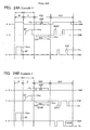
- Figure 4 is a diagram illustrating the first drive method in this embodiment. This is an example of sustaining pulses applied between the X electrodes and Y electrodes.
- Figure 4A illustrates the drive waveforms of the address electrodes A and the X and Y electrodes
- Figure 4B illustrates the path of the discharge current and the drive circuit of the X and Y electrodes.
- the X and Y electrodes are both maintained at a negative first power source potential -V1 that is different from the ground power source GND, and are alternately driven to a positive second power source potential +V2 and then returned to the first power source potential -V1.
- power sources V2 and V1 which use the ground power source GND as a reference, are provided in the drive circuit, and the first power source potential -V1 and second power source +V2 constitute a power source line that is electrically separate from the ground power source line GND.
- the X and Y electrodes may alternatively have different maintenance potentials from separate power sources.
- the drive circuit of the X electrodes comprises N-channel transistors Q5 and Q6, and these transistors are supplied with control signals from the common driver control portion 36.
- the X electrodes are connected to the first power source -V1 via the transistor Q6, and to the second power source +V2 via the transistor Q5.
- the drive circuit of the Y electrodes is provided with a P channel transistor Q1, an N channel transistor Q2, and diodes D1 and D2 for each Y electrode as a scanning driver circuit, and is provided with N channel transistors Q3 and Q4 as a common Y driver. These transistors Q1 and Q2 and diodes D1 and D2 are similarly connected for all of the Y electrodes.
- the transistors Q1 and Q2 are supplied with scanning scan pulses SCPs from the scanning driver control portion 34, and perform an operation whereby scanning pulses are applied to each Y electrode.
- the transistors Q3 and Q4 are supplied with control signals from the common driver control portion 36, and during sustaining discharge there is a connection to the first power source -V1 via the diode D1 and the transistor Q3, and a connection to the second power source +V2 via the diode D2 and the transistor Q4.
- the transistors Q3 and Q6 are conductive and the X and Y electrodes are maintained at the potential of the first power source -V1 in order to perform sustaining discharge. (More accurately, the Y electrodes are maintained at a higher potential than the first power source -V1 by an amount equal to the forward voltage of the diode D1.)
- the transistor Q3 is then turned off and the transistor Q4 turned on, which connects the Y electrodes to the second power source +V2 and applies a discharge pulse. After the pulse period, the transistor Q4 is turned off and the transistor Q3 turned on, and the Y electrodes are once again connected to the first power source -V1.
- the address electrodes are maintained at the ground potential when the sustaining pulses are applied.
- the sustaining pulses are applied by raising the potential of the X and Y electrodes from the potential of the first power source -V1, which is lower than the ground potential, to the potential of the second power source +V2, which is higher than the ground potential, and then returning this potential to that of the first power source -V1. Therefore, only a voltage that is more or less intermediate is applied as the voltage of the sustaining pulses between the address electrodes maintained at the ground potential and the X and Y electrodes. Accordingly, during the application of sustaining pulses, it is possible to prevent the potential of the address electrodes from being too low and excessive positive charges from being stored or colliding forcefully.
- Figure 5 is a diagram illustrating the second drive method in this embodiment.
- the drive circuit in Figure 5B has the same structure as that in Figure 4B.
- Figure 5 is an example of applying sustaining pulses of reverse polarity of Figure 4. Specifically, as shown by the drive waveforms in Figure 5A, the X and Y electrodes are connected to the positive power source +V2, which is higher in potential than the ground potential GND, is driven to the potential of the negative power source -V1, which is lower than the ground potential, and is then returned to the potential of the positive power source +V2.
- the discharge current flows along the path shown in Figure 5B, comprising the positive power source +V2, transistor Q5, the X electrodes, the discharge cells, the Y electrodes, the diode D1, the transistor Q3, and the negative power source -V1. Specifically, no discharge current flows to the ground power source line GND, nor is any noise generated.
- negative drive pulses are applied on the X electrode side, so the discharge current flows along the path shown in Figure 4B, and no discharge current goes into the ground power source GND.
- the address electrodes are maintained at the ground potential, so a large electric field is not applied between the address electrodes and the X and Y electrodes, and negative charges are prevented from colliding or being stored on the address electrode side.
- the potential of the address electrodes is Tower than that of the X and Y electrodes, so positive charges are prevented from colliding with the fluorescent layer.
- FIG. 6 is a diagram illustrating the third drive method in this embodiment.
- drive pulses of reverse polarity are simultaneously applied to the X electrodes and Y electrodes, and applying this combined voltage between the X and Y electrodes generates a discharge.
- the X and Y electrodes are both driven to the potential of the power sources -V3, +V2, and -V1 separate from that of the ground power source GND, so no discharge current flows to the ground power source GND.
- the X and Y electrodes are initially maintained at the potential of the negative power source -V3.
- the Y electrodes are driven to the potential of the positive power source +V2, and at the same time, the X electrodes are driven to the potential of the negative power source -V1.
- the combination of these two drive pulses results in the application of the drive pulses shown in Figures 4 and 5 between the X and Y electrodes.
- the X and Y electrodes are returned to the potential of the power source -V3.
- the drive circuit is shown in Figure 6B.
- the power source -V3 is added to this drive circuit in addition to the drive circuits of Figure 4B and Figure 5B, and transistors Q7, Q8, Q9, and Q10 are also added. These transistors constitute the common electrode drivers 24 and 28 of the respective electrodes, and are supplied with control signals from the corresponding common driver control portion 36.
- the transistors Q9, Q10, Q7, and Q8 are conductive to maintain the X and Y electrodes at the potential of the power source - V3.
- the transistor Q6 is then conductive to connect the X electrodes to the power source -V1
- the transistor Q4 is conductive to connect the Y electrodes to the power source +V2 via the transistor Q4 and the diode D2.
- the discharge current flows through a path comprising the power source +V2, the transistor Q4, the diode D2, the Y electrodes, the discharge cells, the X electrodes, the transistor Q6, and the power source -V1.
- the transistors Q9, Q10, Q7, and Q8 are conductive to return the X and Y electrodes to the potential of the power source -V3.
- the parasitic capacity between the two electrodes is short-circuited, but this short-circuit current also only flows to the power source -V3.
- period t1 even if discharge pulses of reserve polarity are applied to the two electrodes, this will not be accompanied by the generation of noise at the ground power source.
- period t2 the operation is just carried out in completely the opposite polarity as above, and no discharge current or short-circuit current goes into the ground power source, and no noise is generated.
- FIG. 7 is a diagram illustrating the fourth drive method in this embodiment.
- discharge pulses of reverse polarity are applied simultaneously to the X electrodes and Y electrodes, and a discharge is generated by applying the combined voltage thereof between the X and Y electrodes.
- both electrodes are maintained at a state of being at the reference potential of the positive power source +V3, then the Y electrodes are driven to the potential of the positive power source +V2, which is higher than the potential of the positive power source +V3, and the X electrodes are driven to the potential of the negative power source -V1 and then both returned to the reference potential +V3.
- discharge pulses of reverse polarity are applied to both electrodes, and their combined voltage is applied between the two electrodes.
- the drive circuit in Figure 7B is basically the same as that in Figure 6B.
- the discharge current flows through the path shown in the figure, comprising the power source +V2, transistor Q5, the X electrodes, the discharge cells, the Y electrodes, the diode D1, the transistor Q3, and the power source -V1. Accordingly, no discharge current flows to the ground power source GND, and no noise is generated. Even after the completion of the discharge pulses, since the two electrodes are not connected to the ground power source GND, no short-circuit current flows the ground power source.
- the address electrodes are kept at the ground potential, the potential between the address electrodes and the X electrodes and Y electrodes is smaller, making it possible to minimize the problems of wall charge storage on the address electrodes and the collision of positive charges.
- Figure 8 is a diagram illustrating the drive waveform in the first embodiment
- Figure 9 is a diagram illustrating the drive circuit in the first embodiment.
- This embodiment illustrates the constitution of the drive waveforms and drive circuit applied to a three-electrode type of surface discharge AC-PDP.
- the drive waveforms in Figure 8 the drive waveforms of the X and Y electrodes in the sustaining discharge period SUS and the drive waveforms of the two electrodes in the full-write period W are similar to the drive waveforms in the first drive method discussed above.
- the drive circuit utilizes the transistors Q1 and Q2 in the scanning drive of the Y electrodes in the address period, at which time the diodes D1 and D2 are both reverse biased. The rest of the transistors are controlled by the common drive control portion in the full-write and sustaining discharge periods.
- the method for applying sustaining voltage pulses to the display electrodes of the Y electrodes and X electrodes, which are laid out in parallel on the front side is to form sustaining voltage pulses SUSP between the two power source voltages of the power sources-Vs1 and +Vs2, and apply these to the Y and X electrodes.
- the voltage levels for the Y electrodes, the X electrodes, and the address electrodes are first set to the ground potential GND by transistors Q41 and Q42, after which the sustaining period SUS is commenced.
- the voltage levels of both the Y electrodes and the X electrodes are dropped to the power source -Vs1 level, this is set as the reference voltage, and the voltage level of the address electrodes is maintained as the state of the ground potential GND.
- sustaining voltage pulses SUSP of the level of the power source +Vs2 are applied first to the Y electrodes from the reference voltage of the power source -Vs1, which generates a sustaining discharge between the X electrodes and Y electrodes and generates discharge illumination, and at the same time, a peaked gas discharge current flows.
- the discharge current here has been raised to a high potential level on the Y electrode side, so it flows from the supply power source of the power source +Vs2 to the power source - Vs1, going through a switching element Q4 on the Y electrode side, the Y electrodes, the discharge cells, and the X electrodes, and then through a switching element Q6 on the X electrode side.
- the ground terminal side GND of the two power sources +Vs2 and -Vs1 is point-grounded, or is connected to the ground power source GND at close range, which keeps the discharge current from flowing through the ground power source line GND, and therefore the generation of noise that would disrupt the potential of the ground power source GND is prevented.
- a large-capacity capacitor such as an electrolytic capacitor that supplies a charge is usually connected along the wiring path from the power source output to the switching element in order to prevent a voltage drop during the supply of peak current and to compensate the voltage level.
- this capacitor C1 is directly connected between the power source +Vs2 and the power source -Vs1, but is not connected to the ground power source line GND. Doing this prevents the gas discharge current from flowing to the ground power source line GND.
- the potential on the Y electrode side is returned to the potential of the power source -Vs1, which concludes the application of the sustaining voltage pulses SUSP to the Y electrode side.
- the short-circuit current flowing between the two electrodes does not flow through the ground power source line, and only flows to the reference power source -Vs1.
- the sustaining voltage pulses SUSP are similarly applied to the X electrode side in the following timing, but the gas discharge current here just reverses its direction within the panel, and otherwise exactly the same effect is obtained.
- the potential of the address electrode is maintained at the ground potential GND while the above-mentioned sustaining voltage pulses are being continuously applied alternately to the X and Y electrodes. Therefore, the difference in potential between the address electrodes and the sustaining electrodes X and Y is the difference between the ground potential GND and the potential of the power source +Vs2 or the power source -Vs1, and if the absolute value of the power source +Vs2 or -Vs1 is set to be equal, then the potential difference will be cut by half compared to a conventional method, excessive storage of charges on the address electrode can be prevented, and it will be possible to ameliorate malfunctions such as erroneous discharge.
- the same drive method can also be applied to the full-write pulses WP used to periodically activate the display cells over the entire panel.
- the reference voltage -Vw1 is applied all at once to the Y electrodes and X electrodes to lower the potential thereof to the ground potential.
- the potential of the power source +Vwx is then applied to the X electrode side from this reference voltage -Vw1, which generates a full-write discharge.
- the current resulting from this full-write discharge flows within the drive circuit in Figure 9 along the path comprising the switching element Q15 on the X electrode side on the supply power source side of the power source +Vwx, the X electrodes, the discharge cells, and the Y electrodes, and then through the switching elements D1 and Q11 on the Y electrode side to the reference power source-Vw1.
- the ground terminal side of the two power sources +Vwx and -Vw1 is point-grounded, or is connected to the ground power source GND at close range, which keeps the discharge current from flowing through the ground power source line GND. Therefore, there is no generation of noise that would disrupt ground potential GND.
- the Y electrodes and X electrodes both return to the potential of the ground power source GND, and the potential difference between all of the electrodes is reset to zero.
- a flat-wave pulse of the voltage +Vey level is applied from the Y electrode side, this being applied by actuating the switching element Q14 on the Y electrode side, and a flat waveform is obtained by a method in which a transistor Q14 with a higher on-resistance is used, or in which a resistor (not shown) is inserted in series on the output side of the transistor Q14.
- Figure 10 is a diagram illustrating the drive waveform in the second embodiment
- Figure 11 is a diagram illustrating the drive circuit in the second embodiment.
- the same reference numbers will be used to refer to those components that correspond to the first embodiment.
- This second embodiment involves the use of sustaining pulses SUSP or full-write pulses WP with reversed polarity from that in the first embodiment. Also, the write pulses are supplied to the Y electrodes during full-write. Finally, positive power sources +Vw2 and +Vs2 are used as the reference power sources.
- the reference voltage in the sustaining period is set to the power source +Vs2 of positive polarity, and sustaining voltage pulses SUSP of negative polarity whose potential is changed from the level of this power source +Vs2 to the peak voltage -Vs1 is applied to the X and Y electrodes.
- the advantage here is that the voltage pulses generated by the discharge have a potential of negative polarity, so the positive ions of the discharge gas accumulate on the Y and X electrode side, which are the sustaining electrodes, during the discharge generation, and electrons accumulate on the address electrode side across from these electrodes. It is therefore possible to avoid the positive ion collisions with the fluorescent material on the address electrode side that occurred in the past. The benefit in this is a longer service life. Also, a write voltage -Vwy of negative polarity is applied to the Y electrodes from the reference voltage +vw2 of positive polarity in an effort to obtain the same effect in the application of the full-write voltage pulses WP, rather than just the sustaining voltage pulses SUSP.
- Figure 12 is a diagram illustrating the drive waveform in the third embodiment
- Figure 13 is a diagram illustrating the drive circuit in the third embodiment.
- the sustaining period is the same as in the first embodiment ( Figure 8)
- the X and Y electrodes are changed to the negative reference power source -Vs1, and sustaining pulses SUSP of the positive power source +Vs2 are applied thereto.
- the application of the reference voltage during the full-write period is different from that in the first embodiment.
- the transistor Q15 is conductive during full-write to change the X electrodes first to the reference power source +Vw2, and then the transistor Q18 is conductive to change the X electrodes to the power source +Vwx.
- the drive circuit on the Y electrode side is configured the same as in the first embodiment.
- Figure 14 is a diagram illustrating the drive waveform in the fourth embodiment
- Figure 15 is a diagram illustrating the drive circuit in the fourth embodiment.
- the sustaining period is the same as in the second embodiment ( Figure 10)
- the X and Y electrodes are changed to the positive reference power source +Vs2, and sustaining pulses SUSP of the negative power source -Vs1 are applied thereto.
- the application of the reference voltage during the full-write period is different from that in the second embodiment, and is of the opposite polarity as in the third embodiment ( Figure 12).
- the drive during the full-write period is such that separate reference voltages are applied, with the reference voltage -Vw1 of negative polarity to the Y electrodes and the reference voltage +Vw2 of positive polarity to the X electrodes, and the power source -Vwy is applied using the write voltage required for a write operation as the write pulses WP from the Y electrode side. Since reference voltage of opposite polarity is shared as part of the write voltage, the drive voltage of the various electrodes is lower, allowing noise such as higher harmonics to be decreased.
- the drive circuit on the Y electrode side is provided with a transistor Q11 that applies a negative reference power source -Vw1, and a transistor Q19 that applies a negative power source -Vwy for writing.
- the drive circuit on the X electrode side is the same as in the second embodiment ( Figure 11).
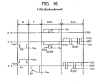
- Figure 16 is a diagram illustrating the drive waveform in the fifth embodiment
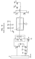
- Figure 17 is a diagram illustrating the drive circuit in the fifth embodiment.
- the sustaining period is the same as in the second embodiment ( Figure 10) and the fourth embodiment ( Figure 14)
- the X and Y electrodes are changed to the positive reference power source +Vs2, and sustaining pulses SUSP of the negative power source -Vs1 are applied thereto.
- the application of the reference voltage during the full-write period, and the application of the write voltage are performed by pulses that are both of opposite polarity with respect to the X and Y electrodes.
- the write pulses were only applied to either the Y electrodes or the X electrodes, but in this embodiment, writing is performed with the combined voltage from both of these electrodes.
- the reference voltage -Vw1 of negative polarity is applied to the Y electrodes and the reference voltage +Vw2 of positive polarity to the X electrodes, after which write pulses Yw of negative polarity and of the level of the power source -Vwy are applied from the Y electrode side, while write pulses Xw of positive polarity and of the level of the power source +Vwx is applied from the X electrode side, and a write discharge is generated by this combined voltage.
- transistors Q15 and Q18 are provided to the drive circuit of the X electrodes, and transistors Q11 and Q19 are provided to the drive circuit of the Y electrodes, making possible the application of the above-mentioned full-write pulses.
- Figure 18 is a diagram illustrating the drive waveform in the sixth embodiment
- Figure 19 is a diagram illustrating the drive circuit in the sixth embodiment.
- the sustaining period and the full-write period are both configured with the same waveforms as in the first embodiment.
- a power source with a similar voltage level is shared in a plurality of drive-use power sources, reducing the types thereof, making the drive circuit more compact, and lowering cost.
- the sustaining voltage of positive polarity is shared with the address voltage Va on the address side
- the sustaining voltage of negative polarity is shared with the Y electrode reference voltage -Vmy in the address period and with the reference voltage -Vmy in the full-write period.
- the number of drive transistors in the drive circuit can also be reduced from that in the first embodiment. Therefore, the overall product is much more compact and inexpensive.
- This sharing of the drive power sources in the sixth embodiment can also be accomplished in the second to fifth embodiments.
- power sources with the same polarity and similar potential can be shared, allowing the power sources and the drive circuit to be simplified.
- Figure 20 is a diagram illustrating the drive waveform in the seventh embodiment
- Figure 21 is a diagram illustrating the drive circuit in the seventh embodiment.
- This example utilizes the third drive method illustrated in Figure 6, and involves the driving of the sustaining discharge and full-write X and Y electrodes.
- the two electrodes are driven from the ground potential to the negative reference power source -Vs1.
- One of the electrodes is driven from this state to the more negative power source -Vs3, and the other electrode is simultaneously driven to the positive power source +Vs2.
- the combination of sustaining pulses applied to the various electrodes results in the voltage-required for sustaining discharge being applied between the two electrodes. This discharge current does not, however, flow to the ground power source GND.
- the two electrodes are driven from the ground potential to the negative reference power source -Vs1.
- the X electrodes are driven to the positive power source +Vwx to apply write pulses Xw
- the Y electrodes are driven to the negative power source -Vwy to apply the write pulses Yw of the opposite polarity.
- the combination of these pulses of opposite polarity results in the application of a sufficiently large write voltage between the two electrodes, and the generation of a full-panel discharge.
- the discharge current does not flow to the ground power source.
- the pulses applied to the various electrodes are also small, so accompanying noise such as higher harmonics can be reduced.
- Figure 21 shows the drive transistors and power sources used to perform the above-mentioned electrode drive. These drive transistors are controlled by a control circuit so as to realize the drive waveforms of Figure 20.
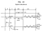
- Figure 22 is a diagram illustrating the drive waveform in the eighth embodiment
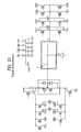
- Figure 23 is a diagram illustrating the drive circuit in the eighth embodiment.
- This example utilizes the fourth drive method illustrated in Figure 7, and involves the driving of the sustaining discharge and full-write X and Y electrodes. Specifically, this drive method has the opposite polarity to that in the seventh embodiment.
- the two electrodes are driven from the ground potential to the positive reference power source +Vs1.
- One of the electrodes is driven from this state to the more positive power source +Vs2, and the other electrode is simultaneously driven to the negative power source -Vs3.
- the combination of sustaining pulses applied to the various electrodes results in the voltage required for sustaining discharge being applied between the two electrodes. This discharge current does not, however, flow to the ground power source GND.
- the two electrodes are driven from the ground potential to the positive reference power source +Vs1.
- the X electrodes are driven to the positive power source +Vwx to apply write pulses Xw
- the Y electrodes are driven to the negative power source -Vwy to apply the write pulses Yw of the opposite polarity.
- the combination of these pulses of opposite polarity results in the application of a sufficiently large write voltage between the two electrodes, and the generation of a full-panel discharge.
- the discharge current does not flow to the ground power source.
- the pulses applied to the various electrodes are also small, so accompanying noise such as higher harmonics can be reduced.
- Figure 23 shows the drive transistors and power sources used to perform the above-mentioned electrode drive. These drive transistors are controlled by a control circuit do as to realize the drive waveforms of Figure 22.
- Embodiments of the present invention were described above using a three-electrode type of surface discharge AC-PDP as an example, but within the scope of the present invention it can be similarly applied to conventional opposing discharge type AC-PDP devices as well.
- the voltage can be kept low between address electrodes and sustain electrodes consisting of X and Y electrodes during gas discharge generation by maintaining the address electrodes at an intermediate potential with respect to the amplitude of the discharge pulses. Therefore, charges can be prevented from accumulating excessively on the dielectric layer surfaces on the address electrode side, and the accompanying erroneous discharges can be prevented.
- drive voltage pulses are applied between a pair of electrodes (X, Y) by driving a first power source (V 2 ) having a specific voltage from a state in which the electrodes are maintained at the potential of a reference power source (V 1 ) that is different from the potential of the ground power source (GND), and then returning it to the reference power source (V 1 ).
- V 2 first power source
- V 1 reference power source
- GND ground power source
- the above-mentioned gas discharge current or capacitance charging and discharging current resulting from the application of the drive voltage pulses flows to the first power source or the reference power source electrically separated from the ground power source, and does not flow to the ground power source line, so no noise is generated on the first power source.
Landscapes
- Engineering & Computer Science (AREA)
- Physics & Mathematics (AREA)
- Power Engineering (AREA)
- Plasma & Fusion (AREA)
- Computer Hardware Design (AREA)
- General Physics & Mathematics (AREA)
- Theoretical Computer Science (AREA)
- Control Of Indicators Other Than Cathode Ray Tubes (AREA)
- Control Of Gas Discharge Display Tubes (AREA)
Applications Claiming Priority (3)
| Application Number | Priority Date | Filing Date | Title |
|---|---|---|---|
| JP37426998A JP3642693B2 (ja) | 1998-12-28 | 1998-12-28 | プラズマディスプレイパネル装置 |
| JP37426998 | 1998-12-28 | ||
| EP99310610A EP1030286A3 (fr) | 1998-12-28 | 1999-12-24 | Panneau d'affichage à plasma |
Related Parent Applications (1)
| Application Number | Title | Priority Date | Filing Date |
|---|---|---|---|
| EP99310610A Division EP1030286A3 (fr) | 1998-12-28 | 1999-12-24 | Panneau d'affichage à plasma |
Publications (2)
| Publication Number | Publication Date |
|---|---|
| EP1426916A2 true EP1426916A2 (fr) | 2004-06-09 |
| EP1426916A3 EP1426916A3 (fr) | 2005-06-22 |
Family
ID=18503557
Family Applications (2)
| Application Number | Title | Priority Date | Filing Date |
|---|---|---|---|
| EP99310610A Withdrawn EP1030286A3 (fr) | 1998-12-28 | 1999-12-24 | Panneau d'affichage à plasma |
| EP03029650A Withdrawn EP1426916A3 (fr) | 1998-12-28 | 1999-12-24 | Circuit d'attaque pour un écran à plasma |
Family Applications Before (1)
| Application Number | Title | Priority Date | Filing Date |
|---|---|---|---|
| EP99310610A Withdrawn EP1030286A3 (fr) | 1998-12-28 | 1999-12-24 | Panneau d'affichage à plasma |
Country Status (5)
| Country | Link |
|---|---|
| US (1) | US7391389B1 (fr) |
| EP (2) | EP1030286A3 (fr) |
| JP (1) | JP3642693B2 (fr) |
| KR (1) | KR100641371B1 (fr) |
| TW (1) | TW498298B (fr) |
Families Citing this family (18)
| Publication number | Priority date | Publication date | Assignee | Title |
|---|---|---|---|---|
| JP2002351388A (ja) | 2001-05-22 | 2002-12-06 | Fujitsu Hitachi Plasma Display Ltd | プラズマディスプレイ装置 |
| JP5031952B2 (ja) * | 2001-06-27 | 2012-09-26 | 株式会社日立製作所 | プラズマディスプレイ |
| JP2003280574A (ja) | 2002-03-26 | 2003-10-02 | Fujitsu Hitachi Plasma Display Ltd | 容量性負荷駆動回路及びプラズマディスプレイ装置 |
| JP4299497B2 (ja) | 2002-05-16 | 2009-07-22 | 日立プラズマディスプレイ株式会社 | 駆動回路 |
| JP2005037604A (ja) * | 2003-07-18 | 2005-02-10 | Matsushita Electric Ind Co Ltd | プラズマディスプレイ装置 |
| FR2860634A1 (fr) | 2003-10-01 | 2005-04-08 | Thomson Plasma | Dispositif de commande d'un panneau d'affichage au plasma |
| KR101042992B1 (ko) * | 2004-03-05 | 2011-06-21 | 엘지전자 주식회사 | 플라즈마 디스플레이 패널의 구동 장치 및 방법 |
| KR100598184B1 (ko) * | 2004-04-09 | 2006-07-10 | 엘지전자 주식회사 | 플라즈마 표시 패널의 구동 장치 |
| JP2005309397A (ja) * | 2004-04-16 | 2005-11-04 | Samsung Sdi Co Ltd | プラズマディスプレイパネル、プラズマディスプレイ装置及びプラズマディスプレイパネルの駆動方法 |
| JP4284295B2 (ja) * | 2004-04-16 | 2009-06-24 | 三星エスディアイ株式会社 | プラズマ表示装置およびプラズマ表示パネルの駆動方法 |
| EP1753262A4 (fr) * | 2004-05-31 | 2010-07-28 | Panasonic Corp | Dispositif d"affichage plasma |
| KR100596235B1 (ko) * | 2004-07-02 | 2006-07-06 | 엘지전자 주식회사 | 플라즈마 표시 패널의 구동 장치 |
| US20060022904A1 (en) * | 2004-07-29 | 2006-02-02 | Lg Electronics Inc. | Plasma display apparatus applying sustain pulse and driving method thereof |
| JP4699146B2 (ja) * | 2004-09-07 | 2011-06-08 | エルジー エレクトロニクス インコーポレイティド | プラズマディスプレイ装置及びその駆動方法 |
| KR101098814B1 (ko) * | 2005-05-24 | 2011-12-26 | 엘지전자 주식회사 | 통합 구동 보드를 갖는 플라즈마 디스플레이 패널 모듈 및그 구동 방법 |
| KR100708692B1 (ko) * | 2005-06-14 | 2007-04-18 | 삼성에스디아이 주식회사 | 디스플레이 패널의 구동장치 |
| KR100739062B1 (ko) * | 2005-10-17 | 2007-07-12 | 삼성에스디아이 주식회사 | 플라즈마 표시 장치 및 그 구동 방법 |
| JPWO2007057957A1 (ja) * | 2005-11-17 | 2009-04-30 | 日立プラズマディスプレイ株式会社 | プラズマディスプレイ装置 |
Citations (3)
| Publication number | Priority date | Publication date | Assignee | Title |
|---|---|---|---|---|
| US4044349A (en) | 1973-09-21 | 1977-08-23 | Fujitsu Limited | Gas discharge panel and method for driving the same |
| US4384287A (en) | 1979-04-11 | 1983-05-17 | Nippon Electric Co., Ltd. | Inverter circuits using insulated gate field effect transistors |
| EP0657861A1 (fr) | 1993-12-10 | 1995-06-14 | Fujitsu Limited | Commande de panneaux d'affichage à plasma à décharge de surface |
Family Cites Families (11)
| Publication number | Priority date | Publication date | Assignee | Title |
|---|---|---|---|---|
| US4370651A (en) | 1981-06-29 | 1983-01-25 | International Business Machines Corporation | Advanced plasma panel technology |
| FR2552575B1 (fr) | 1983-09-27 | 1985-11-08 | Thomson Csf | Circuit de commande d'un panneau a plasma de type alternatif |
| KR940007502B1 (ko) | 1992-03-04 | 1994-08-18 | 삼성전관 주식회사 | 플라즈마 디스플레이 판넬의 구조 및 구동방법 |
| JP2503860B2 (ja) | 1993-04-07 | 1996-06-05 | 日本電気株式会社 | メモリ型プラズマディスプレイパネルの駆動方法 |
| JP2755201B2 (ja) | 1994-09-28 | 1998-05-20 | 日本電気株式会社 | プラズマディスプレイパネルの駆動回路 |
| JPH0922272A (ja) | 1995-07-05 | 1997-01-21 | Oki Electric Ind Co Ltd | 直流型気体放電パネルのメモリ駆動方法 |
| JP3522013B2 (ja) | 1995-09-04 | 2004-04-26 | 富士通株式会社 | 画像表示装置、および画像表示装置の駆動方法 |
| JP3364066B2 (ja) * | 1995-10-02 | 2003-01-08 | 富士通株式会社 | Ac型プラズマディスプレイ装置及びその駆動回路 |
| JP3263310B2 (ja) | 1996-05-17 | 2002-03-04 | 富士通株式会社 | プラズマディスプレイパネル駆動方法及びこの駆動方法を用いたプラズマディスプレイ装置 |
| KR100230437B1 (ko) * | 1997-04-22 | 1999-11-15 | 손욱 | 면 방전형 교류 플라즈마 표시 패널의 구동 방법 |
| JP3365324B2 (ja) * | 1998-10-27 | 2003-01-08 | 日本電気株式会社 | プラズマディスプレイ及びその駆動方法 |
-
1998
- 1998-12-28 JP JP37426998A patent/JP3642693B2/ja not_active Expired - Fee Related
-
1999
- 1999-12-22 US US09/468,639 patent/US7391389B1/en not_active Expired - Fee Related
- 1999-12-22 TW TW088122638A patent/TW498298B/zh not_active IP Right Cessation
- 1999-12-24 EP EP99310610A patent/EP1030286A3/fr not_active Withdrawn
- 1999-12-24 EP EP03029650A patent/EP1426916A3/fr not_active Withdrawn
- 1999-12-27 KR KR1019990062779A patent/KR100641371B1/ko not_active Expired - Fee Related
Patent Citations (3)
| Publication number | Priority date | Publication date | Assignee | Title |
|---|---|---|---|---|
| US4044349A (en) | 1973-09-21 | 1977-08-23 | Fujitsu Limited | Gas discharge panel and method for driving the same |
| US4384287A (en) | 1979-04-11 | 1983-05-17 | Nippon Electric Co., Ltd. | Inverter circuits using insulated gate field effect transistors |
| EP0657861A1 (fr) | 1993-12-10 | 1995-06-14 | Fujitsu Limited | Commande de panneaux d'affichage à plasma à décharge de surface |
Also Published As
| Publication number | Publication date |
|---|---|
| EP1030286A3 (fr) | 2000-12-06 |
| JP3642693B2 (ja) | 2005-04-27 |
| KR100641371B1 (ko) | 2006-10-31 |
| US7391389B1 (en) | 2008-06-24 |
| TW498298B (en) | 2002-08-11 |
| JP2000194316A (ja) | 2000-07-14 |
| EP1030286A2 (fr) | 2000-08-23 |
| EP1426916A3 (fr) | 2005-06-22 |
| KR20000048435A (ko) | 2000-07-25 |
Similar Documents
| Publication | Publication Date | Title |
|---|---|---|
| US6452590B1 (en) | Method and device for driving a display panel | |
| US7391389B1 (en) | Plasma display panel device | |
| KR100275982B1 (ko) | 데이터펄스의충격계수를주기적으로변화시키는드라이버를갖춘표면방전교류플라즈마표시패널의제어방법 | |
| US6160530A (en) | Method and device for driving a plasma display panel | |
| US6281635B1 (en) | Separate voltage driving method and apparatus for plasma display panel | |
| US6215463B1 (en) | Driving system for a display panel | |
| US6211865B1 (en) | Driving apparatus of plasma display panel | |
| US20020089472A1 (en) | Driving method of plasma display panel and circuit thereof | |
| US6727659B2 (en) | Apparatus and method for driving plasma display panels | |
| KR100590112B1 (ko) | 플라즈마 표시 장치 및 그 구동 방법 | |
| US6281633B1 (en) | Plasma display panel driving apparatus | |
| EP1755101A2 (fr) | Appareil d'affichage à plasma | |
| KR100627292B1 (ko) | 플라즈마 표시 장치 및 그 구동 방법 | |
| US7852292B2 (en) | Plasma display apparatus and driving method thereof | |
| US8325110B2 (en) | Power supply and driver for plasma display panel | |
| JP4172539B2 (ja) | プラズマディスプレイパネルの駆動方法および駆動装置 | |
| KR100430089B1 (ko) | 플라즈마 디스플레이 패널의 구동장치 | |
| US8203549B2 (en) | Plasma display panel driving method and plasma display apparatus | |
| KR100645790B1 (ko) | 플라즈마 디스플레이 패널의 구동 장치 | |
| KR100502348B1 (ko) | 플라즈마 디스플레이 패널의 어드레스 구동회로를 위한전력 회생 회로 | |
| KR100453170B1 (ko) | 고주파 플라즈마 디스플레이 패널의 구동방법 및 장치 | |
| KR100811524B1 (ko) | 플라즈마 디스플레이 장치 | |
| US20060192731A1 (en) | Plasma display device | |
| EP1901269A2 (fr) | Appareil d'affichage à plasma | |
| KR19990030777A (ko) | 3전극 면방전 플라즈마 디스플레이 패널의 구동방법 및 그 구동회로 |
Legal Events
| Date | Code | Title | Description |
|---|---|---|---|
| PUAI | Public reference made under article 153(3) epc to a published international application that has entered the european phase |
Free format text: ORIGINAL CODE: 0009012 |
|
| AC | Divisional application: reference to earlier application |
Ref document number: 1030286 Country of ref document: EP Kind code of ref document: P |
|
| AK | Designated contracting states |
Kind code of ref document: A2 Designated state(s): DE FR GB |
|
| PUAL | Search report despatched |
Free format text: ORIGINAL CODE: 0009013 |
|
| AK | Designated contracting states |
Kind code of ref document: A3 Designated state(s): DE FR GB |
|
| RAP1 | Party data changed (applicant data changed or rights of an application transferred) |
Owner name: HITACHI, LTD. |
|
| 17P | Request for examination filed |
Effective date: 20051219 |
|
| AKX | Designation fees paid |
Designated state(s): DE FR GB |
|
| RAP1 | Party data changed (applicant data changed or rights of an application transferred) |
Owner name: HITACHI PLASMA PATENT LICENSING CO., LTD. |
|
| 17Q | First examination report despatched |
Effective date: 20071218 |
|
| STAA | Information on the status of an ep patent application or granted ep patent |
Free format text: STATUS: THE APPLICATION IS DEEMED TO BE WITHDRAWN |
|
| 18D | Application deemed to be withdrawn |
Effective date: 20110701 |