EP1429371A2 - Einrichtung zur Bearbeitung von integrierten Schaltkreisen - Google Patents
Einrichtung zur Bearbeitung von integrierten Schaltkreisen Download PDFInfo
- Publication number
- EP1429371A2 EP1429371A2 EP03016958A EP03016958A EP1429371A2 EP 1429371 A2 EP1429371 A2 EP 1429371A2 EP 03016958 A EP03016958 A EP 03016958A EP 03016958 A EP03016958 A EP 03016958A EP 1429371 A2 EP1429371 A2 EP 1429371A2
- Authority
- EP
- European Patent Office
- Prior art keywords
- carrier
- integrated circuits
- web
- communication means
- communication
- Prior art date
- Legal status (The legal status is an assumption and is not a legal conclusion. Google has not performed a legal analysis and makes no representation as to the accuracy of the status listed.)
- Granted
Links
Images


Classifications
-
- G—PHYSICS
- G06—COMPUTING OR CALCULATING; COUNTING
- G06K—GRAPHICAL DATA READING; PRESENTATION OF DATA; RECORD CARRIERS; HANDLING RECORD CARRIERS
- G06K19/00—Record carriers for use with machines and with at least a part designed to carry digital markings
- G06K19/06—Record carriers for use with machines and with at least a part designed to carry digital markings characterised by the kind of the digital marking, e.g. shape, nature, code
- G06K19/067—Record carriers with conductive marks, printed circuits or semiconductor circuit elements, e.g. credit or identity cards also with resonating or responding marks without active components
- G06K19/07—Record carriers with conductive marks, printed circuits or semiconductor circuit elements, e.g. credit or identity cards also with resonating or responding marks without active components with integrated circuit chips
- G06K19/077—Constructional details, e.g. mounting of circuits in the carrier
- G06K19/07716—Constructional details, e.g. mounting of circuits in the carrier the record carrier comprising means for customization, e.g. being arranged for personalization in batch
-
- G—PHYSICS
- G06—COMPUTING OR CALCULATING; COUNTING
- G06K—GRAPHICAL DATA READING; PRESENTATION OF DATA; RECORD CARRIERS; HANDLING RECORD CARRIERS
- G06K19/00—Record carriers for use with machines and with at least a part designed to carry digital markings
- G06K19/06—Record carriers for use with machines and with at least a part designed to carry digital markings characterised by the kind of the digital marking, e.g. shape, nature, code
- G06K19/067—Record carriers with conductive marks, printed circuits or semiconductor circuit elements, e.g. credit or identity cards also with resonating or responding marks without active components
- G06K19/07—Record carriers with conductive marks, printed circuits or semiconductor circuit elements, e.g. credit or identity cards also with resonating or responding marks without active components with integrated circuit chips
- G06K19/0723—Record carriers with conductive marks, printed circuits or semiconductor circuit elements, e.g. credit or identity cards also with resonating or responding marks without active components with integrated circuit chips the record carrier comprising an arrangement for non-contact communication, e.g. wireless communication circuits on transponder cards, non-contact smart cards or RFIDs
-
- G—PHYSICS
- G06—COMPUTING OR CALCULATING; COUNTING
- G06K—GRAPHICAL DATA READING; PRESENTATION OF DATA; RECORD CARRIERS; HANDLING RECORD CARRIERS
- G06K19/00—Record carriers for use with machines and with at least a part designed to carry digital markings
- G06K19/06—Record carriers for use with machines and with at least a part designed to carry digital markings characterised by the kind of the digital marking, e.g. shape, nature, code
- G06K19/067—Record carriers with conductive marks, printed circuits or semiconductor circuit elements, e.g. credit or identity cards also with resonating or responding marks without active components
- G06K19/07—Record carriers with conductive marks, printed circuits or semiconductor circuit elements, e.g. credit or identity cards also with resonating or responding marks without active components with integrated circuit chips
- G06K19/077—Constructional details, e.g. mounting of circuits in the carrier
- G06K19/07718—Constructional details, e.g. mounting of circuits in the carrier the record carrier being manufactured in a continuous process, e.g. using endless rolls
-
- G—PHYSICS
- G06—COMPUTING OR CALCULATING; COUNTING
- G06K—GRAPHICAL DATA READING; PRESENTATION OF DATA; RECORD CARRIERS; HANDLING RECORD CARRIERS
- G06K7/00—Methods or arrangements for sensing record carriers, e.g. for reading patterns
- G06K7/0008—General problems related to the reading of electronic memory record carriers, independent of its reading method, e.g. power transfer
-
- H—ELECTRICITY
- H05—ELECTRIC TECHNIQUES NOT OTHERWISE PROVIDED FOR
- H05K—PRINTED CIRCUITS; CASINGS OR CONSTRUCTIONAL DETAILS OF ELECTRIC APPARATUS; MANUFACTURE OF ASSEMBLAGES OF ELECTRICAL COMPONENTS
- H05K1/00—Printed circuits
- H05K1/18—Printed circuits structurally associated with non-printed electric components
- H05K1/189—Printed circuits structurally associated with non-printed electric components characterised by the use of flexible or folded printed circuits
-
- H—ELECTRICITY
- H05—ELECTRIC TECHNIQUES NOT OTHERWISE PROVIDED FOR
- H05K—PRINTED CIRCUITS; CASINGS OR CONSTRUCTIONAL DETAILS OF ELECTRIC APPARATUS; MANUFACTURE OF ASSEMBLAGES OF ELECTRICAL COMPONENTS
- H05K3/00—Apparatus or processes for manufacturing printed circuits
- H05K3/0097—Processing two or more printed circuits simultaneously, e.g. made from a common substrate, or temporarily stacked circuit boards
Definitions
- the invention relates to a device for processing integrated Circuits through communication between these and at least one Control unit.
- the invention is based on the object, a device of the above mentioned type in such a way that these with a simple structure a significant larger amount of data per unit time when processing integrated circuits allows.
- the object is in a device of the type mentioned according to the Invention solved by the features in claim 1. Further advantageous Features and embodiments of the invention will become apparent from the dependent claims.
- the invention further consists in a method for processing integrated circuits through communication between these and at least a control unit, wherein the integrated circuits during a predetermined, for their processing sufficient time and / or distance in permanent relative position to at least one communication means of a Be maintained and edited during this phase.
- the integrated circuits together with the communication means z. B. on one Bow path or instead on a straight path without relative movement moved to each other.
- the device is simple and reliable.
- at least one Communication means of the carrier at least one antenna, in particular Coil, provided as antenna, a transmitting / receiving antenna can be provided.
- the respective integrated ones Circuits associated with respective antennas which together with the Circuits arranged on or in the web and thus are parts of the web.
- the at least one Communication means of the carrier from at least one contacting, z.
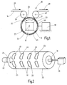
- FIGS. 1 to 3 schematically show a first exemplary embodiment of a device 10 shown, which for the processing of individual in Fig. 3 schematically indicated integrated circuits 11 by communication between the latter and at least one control unit 12 is used.
- the control unit 12 is in Fig. 1 only indicated schematically and consists of an electronic control system, for. B. one Control computer.
- the term "processing" of the integrated circuits 11 includes Any communication, eg. B. the supply of information, reading of information, programming or the like.
- the electric circuits 11 are usually located on a substrate that is not particularly illustrated is.
- the Eiraum 10 according to the first embodiment in Fig. 1 to 3 is for formed contactless communication with the integrated circuits 11, while the device 10 according to the second embodiment in Fig. 4 and 5 for contact-type communication with the integrated circuits 11 is trained.
- the integrated circuits 11 are for the contactless communication with each associated antennas 13 in the form connected by coils, allowing communication with the integrated Circuits 11 via radio is possible.
- the integrated circuits 11 together the associated respective antennas 13 are parts of a web 14.
- the train 14 has z. B. a middle layer into which the integrated circuits 11 with associated antennas 13 are embedded, and also one underneath and above located layer on.
- the integrated circuits 11 with associated antennas 13 Parts of the web 14.
- the web 14 is formed as a continuous web and z. B. made of paper or instead of other suitable or desired Materials. 3 and 5 dashed lines 15 are indicated in the web 14, which should signal that later after processing the integrated Circuits 11 outlined by the lines 15 rectangular Surface areas 16 of the web 14 after cutting individual chip cards 17th form, in the first embodiment with contactless communication contactless chip cards 17 and in the second embodiment according to FIG. 4 and 5 with contact-based communication chip cards 17 are connected to contacts 18, z. B. contact surfaces are provided.
- both embodiments has the web 14, viewed transversely to the web longitudinal direction, a plurality of longitudinal tracks of integrated circuits 11 (FIG. 5) or of integrated circuits 11 each associated with antennas 13 (Fig. 3), wherein in Fig. 3 and Fig. 5, the web 14 in the form of a continuous web, z. B. paper web, shown in planar alignment is.
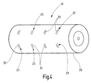
- the device 10 has at least one preferably rotationally symmetrical Carrier 20, the here as a cylinder, z. B. as a drum is formed.
- the carrier 20 is driven in rotation in the direction of arrow 21, wherein the drive z. B. a motor 22, z. B. geared motor od.
- the carrier 20 is at least one, only schematically indicated communication means 23 for communication with the respective integrated circuits 11 equipped.
- the web 14 for example, four longitudinal tracks each with four transverse to Web longitudinal direction juxtaposed integrated circuits 11.
- the carrier 20 is also four identical Communication means 23 provided which are approximately equal in the circumferential direction Are spaced apart from each other and in the direction of the axis of rotation 24 of the Carrier 20 considered viewed at equal transverse intervals from each other like the four longitudinal tracks of the track 14, in particular the respective antennas 13.
- the Track 14 For the processing of the integrated circuits 11 as parts of the web 14 is the Track 14 about the carrier 20, this at a circumferential angle z. From more than Looping around 180 °, guided around (FIG. 1).
- the web 14 is for this purpose in the direction supplied by the arrow 25, deflected by a first guide roller 26, from the latter around the outer cylindrical peripheral surface of the carrier 20 and around hereafter discharged via a second guide roller 27 in the direction of arrow 28. in this connection be the integrated circuits 11 during a predetermined, for the Processing sufficient time and / or distance in permanent Relative position to the at least one communication means 23 of the carrier 20 and edited during this phase.
- the integrated circuits 11 be together with the communication means 23 on one by the cylindrical circumference of the carrier 20 predetermined arc path without Relative movement between the communication means 23 on the one hand and the integrated circuits 11 with antennas 13 on the other hand moves.
- the Processing of the integrated circuits 11 takes place during the Wrap the carrier 20. After processing, the surface areas become 16 of the web, the respective integrated circuits 11 and associated antennas 13 have, along the lines 15 tailored, z. B. is severed, resulting in individual chip cards 17 form, the contactless in the first embodiment are.
- the surface areas 16 of the web 14 may instead also tickets, Labels or other carriers of the integrated circuits 11 associated with Be antennas 13. Due to the fact that the processing of the integrated circuits 11 occurs during the wrapping of the carrier 20, resulting in a relative long residence time of the integrated circuits 11 with antennas 13 on the Circumference of the carrier 20 in the respective area of the associated Communication means 23, so that in the processing of the circuits 11 a large amount of data per unit of time is possible, and this in a very simple and sure way.
- the respective ones are Communication means 23 on the cylindrical circumference of the carrier 20th arranged here z. B. embedded in a cylinder jacket.
- the control unit 12 is z. B. part of the carrier 20 and z. B. arranged in the interior. she runs with the carrier 20 um.
- the respective communication means 23 are available with the Control unit 12 in conjunction.
- the control unit 12 is in turn touching or contactless with at least one stationary, only schematically indicated computer 30 in conjunction, the connection by means of a schematically indicated rotary transmission device 31 z. B. in the form of a Slip ring device, an optical rotary distributor od.
- a schematically indicated rotary transmission device 31 z. B. in the form of a Slip ring device, an optical rotary distributor od.
- the Circumferential motion of the carrier 20 guides the track around the carrier 20 14 together with the carrier 20 a circulating movement without relative movement in With respect to the carrier 20 from.
- the respective communication means 23 of the carrier 20 consists of at least an antenna 32, which is indicated only schematically in Fig. 2 and from a each coil consists. In appropriate assignment has each circuit 11 a respective antenna 13 on the web 14 and in the web 14th
- each communication means 23 is off at least one contacting device 33 formed with the contacts 18 respective associated integrated circuits 11 of the web 14 for the Processing of the circuits 11 comes into contact. Otherwise, the Operation of the device 10 the same as in the first embodiment.
- a plurality of carriers 20, in particular cylinder, in an arrangement next to each other and / or be provided one behind the other, these multiple carriers to a machine can be assembled.
- the plurality of carriers 20 may be contactless communication means 23 and / or for contact-type communication. This implies that multiple carriers 20 either similar communication means 23, z. B. in shape of antennas 32 or instead in the form of contactors 33, or alternatively with a mixture of contactless or contact-based communication means 23, d. H. Antennas 32 and Contacting devices 33, may be provided.
- the integrated Circuits 11 together with the communication means 23 also on a straight track 14 instead of on a curved path without relative movement to each other moved and edited during this phase.
Landscapes
- Engineering & Computer Science (AREA)
- Physics & Mathematics (AREA)
- General Physics & Mathematics (AREA)
- Theoretical Computer Science (AREA)
- Computer Hardware Design (AREA)
- Microelectronics & Electronic Packaging (AREA)
- Computer Vision & Pattern Recognition (AREA)
- Artificial Intelligence (AREA)
- Computer Networks & Wireless Communication (AREA)
- Near-Field Transmission Systems (AREA)
- Hardware Redundancy (AREA)
- Semiconductor Integrated Circuits (AREA)
- Credit Cards Or The Like (AREA)
- Exchange Systems With Centralized Control (AREA)
- Rotary Presses (AREA)
- Folding Of Thin Sheet-Like Materials, Special Discharging Devices, And Others (AREA)
- Inking, Control Or Cleaning Of Printing Machines (AREA)
- Optical Communication System (AREA)
Abstract
Description
- Fig. 1
- eine schematische, teilweise geschnittene Seitenansicht der wesentlichen Teile einer Einrichtung zur Bearbeitung von integrierten Schaltkreisen gemäß einem ersten Ausführungsbeispiel,
- Fig. 2
- eine schematische perspektivische Ansicht des rotationssymmetrischen Trägers der Einrichtung in Fig. 1,
- Fig. 3
- eine schematische Draufsicht einer Bahn gemäß dem ersten Ausführungsbeispiel, in die integrierte Schaltkreise und zugeordnete Antennen eingearbeitet sind,
- Fig. 4
- eine schematische perspektivische Ansicht eines Trägers einer Einrichtung gemäß einem zweiten Ausführungsbeispiel,
- Fig. 5
- eine schematische Draufsicht einer Bahn gemäß einem zweiten Ausführungsbeispiel, in die kontaktbehaftete integrierte Schaltkreise eingearbeitet sind.
Claims (25)
- Einrichtung zur Bearbeitung von integrierten Schaltkreisen (11) durch Kommunikation zwischen diesen und mindestens einer Steuereinheit (12),
gekennzeichnet durch
mindestens einen umlaufend angetriebenen rotationssymmetrischen Träger (20) mit mindestens einem Kommunikationsmittel (23) zur Kommunikation mit den integrierten Schaltkreisen (11), wobei die letzteren (11) Teile einer um den Träger (20) herumgeführten Bahn (14) sind. - Einrichtung nach Anspruch 1,
dadurch gekennzeichnet, dass der Träger (20) mehrere in Umfangsrichtung in etwa gleichen Abständen voneinander angeordnete Kommunikationsmittel (23) aufweist. - Einrichtung nach Anspruch 1 oder 2,
dadurch gekennzeichnet, dass der Träger (20), in Richtung seiner Drehachse (24) betrachtet, mehrere in etwa gleichen Querabständen voneinander angeordnete Längsspuren mit jeweiligen Kommunikationsmitteln (23) aufweist. - Einrichtung nach einem der Ansprüche 1 bis 3,
dadurch gekennzeichnet, dass die jeweiligen Kommunikationsmittel (23) auf dem zylindrischen Umfang des Trägers (20) angeordnet sind, z. B. in einen Zylindermantel eingebettet sind. - Einrichtung nach einem der Ansprüche 1 bis 4,
dadurch gekennzeichnet, dass die mindestens eine Steuereinheit (12) Teil des Trägers (20) ist und mit diesem umläuft. - Einrichtung nach einem der Ansprüche 1 bis 5,
dadurch gekennzeichnet, dass die jeweiligen Kommunikationsmittel (23) des Trägers (20) mit der Steuereinheit (12) in Verbindung stehen. - Einrichtung nach einem der Ansprüche 1 bis 6,
dadurch gekennzeichnet, dass die mindestens eine Steuereinheit (12) im Inneren des Trägers (20) angeordnet ist. - Einrichtung nach einem der Ansprüche 1 bis 7,
dadurch gekennzeichnet, dass die mindestens eine mit dem Träger (20) umlaufende Steuereinheit (12) berührend oder berührungslos mit mindestens einem zugeordneten stationären Rechner (30) in Verbindung steht. - Einrichtung nach Anspruch 8,
dadurch gekennzeichnet, dass die Steuereinheit (12) mittels einer Drehübertragungseinrichtung (31), z.B. einer Schleifringeinrichtung, eines optischen Drehverteilers od. dgl., mit dem stationären Rechner (30) in Verbindung steht. - Einrichtung nach einem der Ansprüche 1 bis 9,
dadurch gekennzeichnet, dass der Träger (20) als Zylinder, z.B. als Trommel, ausgebildet ist. - Einrichtung nach einem der Ansprüche 1 bis 10,
dadurch gekennzeichnet, dass die integrierten Schaltkreise (11) auf der Bahn (14) aufgebracht sind oder in die Bahn (14) eingearbeitet sind. - Einrichtung nach einem der Ansprüche 1 bis 11,
dadurch gekennzeichnet, dass die um den Träger (20) herumgeführte Bahn (14) als Endlosbahn, z. B. Papierbahn, ausgebildet ist. - Einrichtung nach einem der Ansprüche 1 bis 12,
dadurch gekennzeichnet, dass die um den Träger (20) herumgeführte Bahn (14) zusammen mit dem Träger (20) eine Umlaufbewegung ohne Relativbewegung zwischen diesen ausführt. - Einrichtung nach einem der Ansprüche 1 bis 13,
dadurch gekennzeichnet, dass die Bahn (14), quer zur Bahnlängsrichtung betrachtet, mehrere in etwa gleichen Querabständen voneinander angeordnete Längsspuren von integrierten Schaltkreisen (11) aufweist. - Einrichtung nach einem der Ansprüche 1 bis 14,
dadurch gekennzeichnet, dass der jeweilige Abstand der einzelnen in Umfangsrichtung des Trägers (20) aufeinanderfolgenden Kommunikationsmittel (23) voneinander, auf eine Gerade abgewickelt, ebenso groß bemessen ist wie der Abstand, den die in Bahnlängsrichtung in Abständen aufeinanderfolgenden integrierten Schaltkreise (11) voneinander aufweisen. - Einrichtung nach einem der Ansprüche 1 bis 15,
dadurch gekennzeichnet, dass die Kommunikationsmittel (23) und die integrierten Schaltkreise (11) zur kontaktlosen und/oder kontaktbehafteten Kommunikation ausgebildet sind. - Einrichtung nach Anspruch 16,
dadurch gekennzeichnet, dass für die berührungslose Kommunikation das mindestens eine Kommunikationsmittel (23) des Trägers (20) aus mindestens einer Antenne (32), insbesondere Spule, gebildet ist und dass dem jeweiligen integrierten Schaltkreis (11) ebenfalls eine jeweilige Antenne (13), insbesondere Spule, auf oder in der Bahn (14) zugeordnet ist. - Einrichtung nach Anspruch 16,
dadurch gekennzeichnet, dass für die berührende Kommunikation das mindestens eine Kommunikationsmittel (23) des Trägers (20) aus mindestens einer Kontaktiereinrichtung (33) gebildet ist und dass der jeweilige integrierte Schaltkreis (11) mit Kontakten (18), insbesondere Kontaktflächen, versehen ist. - Einrichtung nach Anspruch 17,
dadurch gekennzeichnet, dass Flächenbereiche (16) der Bahn (14), die jeweils integrierte Schaltkreise (11) und zugeordnete Antennen (13) aufweisen, nach ihrem Zuschneiden einzelne kontaktlose Chipkarten (17) bilden. - Einrichtung nach Anspruch 18,
dadurch gekennzeichnet, dass Flächenbereiche (16) der Bahn (14), die jeweils integrierte Schaltkreise (11) aufweisen, nach ihrem Zuschneiden einzelne kontaktbehaftete Chipkarten (17) bilden. - Einrichtung nach einem der Ansprüche 1 bis 20,
dadurch gekennzeichnet, dass mehrere Träger (20), insbesondere Zylinder, in Anordnung nebeneinander und/oder hintereinander vorgesehen sind. - Einrichtung nach Anspruch 21,
dadurch gekennzeichnet, dass die mehreren Träger (20) Kommunikationsmittel (23) für kontaktlose und/oder kontaktbehaftete Kommunikation aufweisen. - Verfahren zur Bearbeitung von integrierten Schaltkreisen (11) durch Kommunikation zwischen diesen und mindestens einer Steuereinheit (12),
dadurch gekennzeichnet, dass die integrierten Schaltkreise (11) während einer vorgegebenen, für deren Bearbeitung ausreichenden Zeit und/oder Wegstrecke in bleibender Relativposition zu mindestes einem Kommunikationsmittel (23) eines Trägers (20) gehalten und während dieser Phase bearbeitet werden. - Verfahren nach Anspruch 23,
dadurch gekennzeichnet, dass die integrierten Schaltkreise (11) zusammen mit den Kommunikationsmitteln (23) auf einer Bogenbahn ohne Relativbewegung zueinander bewegt werden. - Verfahren nach Anspruch 23,
dadurch gekennzeichnet, dass die integrierten Schaltkreise (11) zusammen mit den Kommunikationsmitteln (23) auf einer geraden Bahn (14) ohne Relativbewegung zueinander bewegt werden.
Priority Applications (1)
| Application Number | Priority Date | Filing Date | Title |
|---|---|---|---|
| US10/655,181 US7004400B2 (en) | 2002-12-11 | 2003-09-04 | Device for and method of processing integrated circuits |
Applications Claiming Priority (2)
| Application Number | Priority Date | Filing Date | Title |
|---|---|---|---|
| DE10257777A DE10257777A1 (de) | 2002-12-11 | 2002-12-11 | Einrichtung zur Bearbeitung von integrierten Schaltkreisen |
| DE10257777 | 2002-12-11 |
Publications (3)
| Publication Number | Publication Date |
|---|---|
| EP1429371A2 true EP1429371A2 (de) | 2004-06-16 |
| EP1429371A3 EP1429371A3 (de) | 2005-08-17 |
| EP1429371B1 EP1429371B1 (de) | 2009-04-08 |
Family
ID=32319038
Family Applications (1)
| Application Number | Title | Priority Date | Filing Date |
|---|---|---|---|
| EP03016958A Expired - Lifetime EP1429371B1 (de) | 2002-12-11 | 2003-07-25 | Einrichtung zur Bearbeitung von integrierten Schaltkreisen |
Country Status (7)
| Country | Link |
|---|---|
| EP (1) | EP1429371B1 (de) |
| CN (1) | CN1320495C (de) |
| AT (1) | ATE428183T1 (de) |
| CA (1) | CA2442211C (de) |
| DE (2) | DE10257777A1 (de) |
| ES (1) | ES2323053T3 (de) |
| IL (1) | IL157384A0 (de) |
Cited By (1)
| Publication number | Priority date | Publication date | Assignee | Title |
|---|---|---|---|---|
| WO2006131439A1 (de) * | 2005-06-06 | 2006-12-14 | Mühlbauer Ag | Vorrichtung und verfahren zum lesen und/oder schreiben von daten von und/oder auf eine(r) vielzahl von rfid-chips |
Family Cites Families (3)
| Publication number | Priority date | Publication date | Assignee | Title |
|---|---|---|---|---|
| US5563095A (en) * | 1994-12-01 | 1996-10-08 | Frey; Jeffrey | Method for manufacturing semiconductor devices |
| ES2221027T3 (es) * | 1996-08-09 | 2004-12-16 | Ferag Ag | Objeto movil de datos electronicos memorizados que pueden ser leidos y/o registrados sin contacto. |
| FR2766945B1 (fr) * | 1997-07-29 | 1999-10-29 | Leroux Gilles Sa | Machine de personnalisation a haute cadence |
-
2002
- 2002-12-11 DE DE10257777A patent/DE10257777A1/de not_active Withdrawn
-
2003
- 2003-07-25 ES ES03016958T patent/ES2323053T3/es not_active Expired - Lifetime
- 2003-07-25 AT AT03016958T patent/ATE428183T1/de not_active IP Right Cessation
- 2003-07-25 DE DE50311386T patent/DE50311386D1/de not_active Expired - Lifetime
- 2003-07-25 EP EP03016958A patent/EP1429371B1/de not_active Expired - Lifetime
- 2003-08-13 IL IL15738403A patent/IL157384A0/xx unknown
- 2003-09-24 CA CA2442211A patent/CA2442211C/en not_active Expired - Fee Related
- 2003-10-28 CN CNB2003101026585A patent/CN1320495C/zh not_active Expired - Fee Related
Cited By (2)
| Publication number | Priority date | Publication date | Assignee | Title |
|---|---|---|---|---|
| WO2006131439A1 (de) * | 2005-06-06 | 2006-12-14 | Mühlbauer Ag | Vorrichtung und verfahren zum lesen und/oder schreiben von daten von und/oder auf eine(r) vielzahl von rfid-chips |
| US8022828B2 (en) | 2005-06-06 | 2011-09-20 | Muehlbauer Ag | Device and method for reading and/or writing data from and/or to a multiplicity of RFID chips |
Also Published As
| Publication number | Publication date |
|---|---|
| CA2442211A1 (en) | 2004-06-11 |
| IL157384A0 (en) | 2004-02-19 |
| DE50311386D1 (de) | 2009-05-20 |
| DE10257777A1 (de) | 2004-06-24 |
| CA2442211C (en) | 2012-12-18 |
| EP1429371A3 (de) | 2005-08-17 |
| ATE428183T1 (de) | 2009-04-15 |
| ES2323053T3 (es) | 2009-07-06 |
| CN1507029A (zh) | 2004-06-23 |
| CN1320495C (zh) | 2007-06-06 |
| EP1429371B1 (de) | 2009-04-08 |
Similar Documents
| Publication | Publication Date | Title |
|---|---|---|
| WO1983004448A1 (fr) | Dispositif d'identification en forme d'etiquette pouvant etre appliquee sur un objet et son procede de fabrication | |
| EP1678744B1 (de) | Positionierungsvorrichtung und verfahren für die übertragung elektronischer bauteile | |
| EP1435587A2 (de) | Vorrichtung zum Bearbeiten kartenförmiger Informationsträger, wie Scheckkarten, Kreditkarten oder Ausweiskarten | |
| EP1328899B1 (de) | Verfahren zur herstellung einer transponderspule | |
| DE2821987A1 (de) | Markierungsleser | |
| EP3461352B1 (de) | Vorrichtung zur bearbeitung von artikeln der tabak verarbeitenden industrie | |
| EP1560155B1 (de) | Verfahren zur Herstellung von kontaklosen Chip-Karten | |
| EP0287874A1 (de) | Vorrichtung zum Erfassen und Steuern des Geradlaufs eines angetriebenen Transportbands | |
| EP0999015B1 (de) | Bahnschneidvorrichtung mit einer integrierten Messeranordnung in einer Rollenrotationsdruckmaschine | |
| EP1217575A2 (de) | Verfahren zum Bearbeiten, insbesondere Lesen, Programmieren od.dgl., kartenförmiger Informationsträger | |
| EP1429371A2 (de) | Einrichtung zur Bearbeitung von integrierten Schaltkreisen | |
| DE102005054300B3 (de) | Verfahren und Vorrichtung zum simultanen Beschreiben von Datenträgern | |
| DE10102540A1 (de) | Anordnung und Verfahren zur Identifikation von Substraten | |
| DE19734855A1 (de) | Aufbau beugungsoptisch wirksamer Sicherheitselemente und Vorrichtung zur Prüfung derartiger Elemente | |
| DE102005035848B4 (de) | Vorrichtung und Verfahren zum Lesen und/oder Schreiben von Daten von und/oder auf eine(r) Vielzahl von RFID-Chips | |
| DE602006001034T2 (de) | Funkübertragungssystem, Antennenvorrichtung und Verfahren zur Bogenbearbeitung | |
| DE3806170C2 (de) | Verfahren und Vorrichtung zum Durchlaufabisolieren von dünnen, mit hochwarmfestem Lack isolierten Drähten | |
| DE102018003123B4 (de) | Verwendung einer Anordnung zur Überwachung von Werkzeugen bei der Bearbeitung rotationssymmetrischer Werkstücke | |
| EP2036006B1 (de) | Chipkarte und verfahren zur herstellung einer chipkarte | |
| EP1029820A2 (de) | Vorrichtung zum Umlenken von Bogen | |
| EP4061643B1 (de) | Verfahren zur herstellung von banknoten mit jeweils mindestens einer integrierten schaltung | |
| DE102023118245A1 (de) | Kontaktierungseinheit für ein Umwindegarn, elektrisch kontaktierbares Umwindegarn sowie Verfahren zu dessen Herstellung | |
| DE102023212362A1 (de) | Verfahren zur ortsgenauen Behandlung eines mehrschichtigen Endlosprodukts | |
| DE4442917C2 (de) | Verfahren zum Aufbringen von Magnetmarken | |
| DE19948955A1 (de) | Bahnschneidvorrichtung mit einer integrierten Messeranordnung in einer Rollenrotationsdruckmaschine |
Legal Events
| Date | Code | Title | Description |
|---|---|---|---|
| PUAI | Public reference made under article 153(3) epc to a published international application that has entered the european phase |
Free format text: ORIGINAL CODE: 0009012 |
|
| AK | Designated contracting states |
Kind code of ref document: A2 Designated state(s): AT BE BG CH CY CZ DE DK EE ES FI FR GB GR HU IE IT LI LU MC NL PT RO SE SI SK TR |
|
| AX | Request for extension of the european patent |
Extension state: AL LT LV MK |
|
| PUAL | Search report despatched |
Free format text: ORIGINAL CODE: 0009013 |
|
| AK | Designated contracting states |
Kind code of ref document: A3 Designated state(s): AT BE BG CH CY CZ DE DK EE ES FI FR GB GR HU IE IT LI LU MC NL PT RO SE SI SK TR |
|
| AX | Request for extension of the european patent |
Extension state: AL LT LV MK |
|
| 17P | Request for examination filed |
Effective date: 20051217 |
|
| AKX | Designation fees paid |
Designated state(s): AT BE BG CH CY CZ DE DK EE ES FI FR GB GR HU IE IT LI LU MC NL PT RO SE SI SK TR |
|
| 17Q | First examination report despatched |
Effective date: 20060828 |
|
| GRAP | Despatch of communication of intention to grant a patent |
Free format text: ORIGINAL CODE: EPIDOSNIGR1 |
|
| GRAS | Grant fee paid |
Free format text: ORIGINAL CODE: EPIDOSNIGR3 |
|
| GRAA | (expected) grant |
Free format text: ORIGINAL CODE: 0009210 |
|
| AK | Designated contracting states |
Kind code of ref document: B1 Designated state(s): AT BE BG CH CY CZ DE DK EE ES FI FR GB GR HU IE IT LI LU MC NL PT RO SE SI SK TR |
|
| REG | Reference to a national code |
Ref country code: GB Ref legal event code: FG4D Free format text: NOT ENGLISH |
|
| REG | Reference to a national code |
Ref country code: CH Ref legal event code: NV Representative=s name: PATENTANWALTSBUERO JEAN HUNZIKER AG Ref country code: CH Ref legal event code: EP |
|
| REG | Reference to a national code |
Ref country code: IE Ref legal event code: FG4D |
|
| REF | Corresponds to: |
Ref document number: 50311386 Country of ref document: DE Date of ref document: 20090520 Kind code of ref document: P |
|
| REG | Reference to a national code |
Ref country code: ES Ref legal event code: FG2A Ref document number: 2323053 Country of ref document: ES Kind code of ref document: T3 |
|
| PG25 | Lapsed in a contracting state [announced via postgrant information from national office to epo] |
Ref country code: SI Free format text: LAPSE BECAUSE OF FAILURE TO SUBMIT A TRANSLATION OF THE DESCRIPTION OR TO PAY THE FEE WITHIN THE PRESCRIBED TIME-LIMIT Effective date: 20090408 |
|
| NLV1 | Nl: lapsed or annulled due to failure to fulfill the requirements of art. 29p and 29m of the patents act | ||
| REG | Reference to a national code |
Ref country code: IE Ref legal event code: FD4D |
|
| PG25 | Lapsed in a contracting state [announced via postgrant information from national office to epo] |
Ref country code: PT Free format text: LAPSE BECAUSE OF FAILURE TO SUBMIT A TRANSLATION OF THE DESCRIPTION OR TO PAY THE FEE WITHIN THE PRESCRIBED TIME-LIMIT Effective date: 20090908 Ref country code: FI Free format text: LAPSE BECAUSE OF FAILURE TO SUBMIT A TRANSLATION OF THE DESCRIPTION OR TO PAY THE FEE WITHIN THE PRESCRIBED TIME-LIMIT Effective date: 20090408 |
|
| PG25 | Lapsed in a contracting state [announced via postgrant information from national office to epo] |
Ref country code: SE Free format text: LAPSE BECAUSE OF FAILURE TO SUBMIT A TRANSLATION OF THE DESCRIPTION OR TO PAY THE FEE WITHIN THE PRESCRIBED TIME-LIMIT Effective date: 20090708 Ref country code: NL Free format text: LAPSE BECAUSE OF FAILURE TO SUBMIT A TRANSLATION OF THE DESCRIPTION OR TO PAY THE FEE WITHIN THE PRESCRIBED TIME-LIMIT Effective date: 20090408 |
|
| PG25 | Lapsed in a contracting state [announced via postgrant information from national office to epo] |
Ref country code: IE Free format text: LAPSE BECAUSE OF FAILURE TO SUBMIT A TRANSLATION OF THE DESCRIPTION OR TO PAY THE FEE WITHIN THE PRESCRIBED TIME-LIMIT Effective date: 20090408 Ref country code: DK Free format text: LAPSE BECAUSE OF FAILURE TO SUBMIT A TRANSLATION OF THE DESCRIPTION OR TO PAY THE FEE WITHIN THE PRESCRIBED TIME-LIMIT Effective date: 20090408 Ref country code: CZ Free format text: LAPSE BECAUSE OF FAILURE TO SUBMIT A TRANSLATION OF THE DESCRIPTION OR TO PAY THE FEE WITHIN THE PRESCRIBED TIME-LIMIT Effective date: 20090408 Ref country code: RO Free format text: LAPSE BECAUSE OF FAILURE TO SUBMIT A TRANSLATION OF THE DESCRIPTION OR TO PAY THE FEE WITHIN THE PRESCRIBED TIME-LIMIT Effective date: 20090408 Ref country code: EE Free format text: LAPSE BECAUSE OF FAILURE TO SUBMIT A TRANSLATION OF THE DESCRIPTION OR TO PAY THE FEE WITHIN THE PRESCRIBED TIME-LIMIT Effective date: 20090408 |
|
| BERE | Be: lapsed |
Owner name: ATLANTIC ZEISER G.M.B.H. Effective date: 20090731 |
|
| PLBE | No opposition filed within time limit |
Free format text: ORIGINAL CODE: 0009261 |
|
| STAA | Information on the status of an ep patent application or granted ep patent |
Free format text: STATUS: NO OPPOSITION FILED WITHIN TIME LIMIT |
|
| PG25 | Lapsed in a contracting state [announced via postgrant information from national office to epo] |
Ref country code: SK Free format text: LAPSE BECAUSE OF FAILURE TO SUBMIT A TRANSLATION OF THE DESCRIPTION OR TO PAY THE FEE WITHIN THE PRESCRIBED TIME-LIMIT Effective date: 20090408 Ref country code: MC Free format text: LAPSE BECAUSE OF NON-PAYMENT OF DUE FEES Effective date: 20090731 |
|
| 26N | No opposition filed |
Effective date: 20100111 |
|
| PG25 | Lapsed in a contracting state [announced via postgrant information from national office to epo] |
Ref country code: BG Free format text: LAPSE BECAUSE OF FAILURE TO SUBMIT A TRANSLATION OF THE DESCRIPTION OR TO PAY THE FEE WITHIN THE PRESCRIBED TIME-LIMIT Effective date: 20090708 |
|
| PG25 | Lapsed in a contracting state [announced via postgrant information from national office to epo] |
Ref country code: BE Free format text: LAPSE BECAUSE OF NON-PAYMENT OF DUE FEES Effective date: 20090731 |
|
| PG25 | Lapsed in a contracting state [announced via postgrant information from national office to epo] |
Ref country code: GR Free format text: LAPSE BECAUSE OF FAILURE TO SUBMIT A TRANSLATION OF THE DESCRIPTION OR TO PAY THE FEE WITHIN THE PRESCRIBED TIME-LIMIT Effective date: 20090709 |
|
| PG25 | Lapsed in a contracting state [announced via postgrant information from national office to epo] |
Ref country code: AT Free format text: LAPSE BECAUSE OF NON-PAYMENT OF DUE FEES Effective date: 20090725 |
|
| PG25 | Lapsed in a contracting state [announced via postgrant information from national office to epo] |
Ref country code: LU Free format text: LAPSE BECAUSE OF NON-PAYMENT OF DUE FEES Effective date: 20090725 |
|
| PG25 | Lapsed in a contracting state [announced via postgrant information from national office to epo] |
Ref country code: HU Free format text: LAPSE BECAUSE OF FAILURE TO SUBMIT A TRANSLATION OF THE DESCRIPTION OR TO PAY THE FEE WITHIN THE PRESCRIBED TIME-LIMIT Effective date: 20091009 |
|
| PG25 | Lapsed in a contracting state [announced via postgrant information from national office to epo] |
Ref country code: TR Free format text: LAPSE BECAUSE OF FAILURE TO SUBMIT A TRANSLATION OF THE DESCRIPTION OR TO PAY THE FEE WITHIN THE PRESCRIBED TIME-LIMIT Effective date: 20090408 |
|
| PG25 | Lapsed in a contracting state [announced via postgrant information from national office to epo] |
Ref country code: CY Free format text: LAPSE BECAUSE OF FAILURE TO SUBMIT A TRANSLATION OF THE DESCRIPTION OR TO PAY THE FEE WITHIN THE PRESCRIBED TIME-LIMIT Effective date: 20090408 |
|
| REG | Reference to a national code |
Ref country code: DE Ref legal event code: R082 Ref document number: 50311386 Country of ref document: DE Representative=s name: MAS&P MIESS, ALTHERR, SIBINGER & PARTNER, PART, DE |
|
| REG | Reference to a national code |
Ref country code: FR Ref legal event code: PLFP Year of fee payment: 13 |
|
| REG | Reference to a national code |
Ref country code: FR Ref legal event code: PLFP Year of fee payment: 14 |
|
| PGFP | Annual fee paid to national office [announced via postgrant information from national office to epo] |
Ref country code: GB Payment date: 20160722 Year of fee payment: 14 Ref country code: IT Payment date: 20160721 Year of fee payment: 14 Ref country code: CH Payment date: 20160726 Year of fee payment: 14 Ref country code: DE Payment date: 20160512 Year of fee payment: 14 |
|
| PGFP | Annual fee paid to national office [announced via postgrant information from national office to epo] |
Ref country code: FR Payment date: 20160722 Year of fee payment: 14 |
|
| PGFP | Annual fee paid to national office [announced via postgrant information from national office to epo] |
Ref country code: ES Payment date: 20160722 Year of fee payment: 14 |
|
| REG | Reference to a national code |
Ref country code: DE Ref legal event code: R119 Ref document number: 50311386 Country of ref document: DE |
|
| REG | Reference to a national code |
Ref country code: CH Ref legal event code: PL |
|
| GBPC | Gb: european patent ceased through non-payment of renewal fee |
Effective date: 20170725 |
|
| REG | Reference to a national code |
Ref country code: FR Ref legal event code: ST Effective date: 20180330 |
|
| PG25 | Lapsed in a contracting state [announced via postgrant information from national office to epo] |
Ref country code: GB Free format text: LAPSE BECAUSE OF NON-PAYMENT OF DUE FEES Effective date: 20170725 Ref country code: LI Free format text: LAPSE BECAUSE OF NON-PAYMENT OF DUE FEES Effective date: 20170731 Ref country code: DE Free format text: LAPSE BECAUSE OF NON-PAYMENT OF DUE FEES Effective date: 20180201 Ref country code: CH Free format text: LAPSE BECAUSE OF NON-PAYMENT OF DUE FEES Effective date: 20170731 |
|
| PG25 | Lapsed in a contracting state [announced via postgrant information from national office to epo] |
Ref country code: FR Free format text: LAPSE BECAUSE OF NON-PAYMENT OF DUE FEES Effective date: 20170731 |
|
| PG25 | Lapsed in a contracting state [announced via postgrant information from national office to epo] |
Ref country code: IT Free format text: LAPSE BECAUSE OF NON-PAYMENT OF DUE FEES Effective date: 20170725 |
|
| REG | Reference to a national code |
Ref country code: ES Ref legal event code: FD2A Effective date: 20181030 |
|
| PG25 | Lapsed in a contracting state [announced via postgrant information from national office to epo] |
Ref country code: ES Free format text: LAPSE BECAUSE OF NON-PAYMENT OF DUE FEES Effective date: 20170726 |