EP1430596B1 - Circuit amplificateur thermostable - Google Patents
Circuit amplificateur thermostable Download PDFInfo
- Publication number
- EP1430596B1 EP1430596B1 EP02754418A EP02754418A EP1430596B1 EP 1430596 B1 EP1430596 B1 EP 1430596B1 EP 02754418 A EP02754418 A EP 02754418A EP 02754418 A EP02754418 A EP 02754418A EP 1430596 B1 EP1430596 B1 EP 1430596B1
- Authority
- EP
- European Patent Office
- Prior art keywords
- current
- gain factor
- amplifier circuit
- iref
- amplifier
- Prior art date
- Legal status (The legal status is an assumption and is not a legal conclusion. Google has not performed a legal analysis and makes no representation as to the accuracy of the status listed.)
- Expired - Lifetime
Links
- 230000003321 amplification Effects 0.000 claims description 11
- 238000003199 nucleic acid amplification method Methods 0.000 claims description 11
- 230000001419 dependent effect Effects 0.000 claims description 7
- 238000000034 method Methods 0.000 claims description 5
- 239000000758 substrate Substances 0.000 claims description 2
- 238000004519 manufacturing process Methods 0.000 description 7
- 229910021420 polycrystalline silicon Inorganic materials 0.000 description 5
- 229920005591 polysilicon Polymers 0.000 description 5
- 238000010586 diagram Methods 0.000 description 4
- 238000013459 approach Methods 0.000 description 3
- 230000007423 decrease Effects 0.000 description 2
- 230000008021 deposition Effects 0.000 description 2
- 230000000694 effects Effects 0.000 description 2
- 239000000463 material Substances 0.000 description 2
- 230000005540 biological transmission Effects 0.000 description 1
- 230000000295 complement effect Effects 0.000 description 1
- 230000002596 correlated effect Effects 0.000 description 1
- 238000013461 design Methods 0.000 description 1
- 238000011161 development Methods 0.000 description 1
- 230000018109 developmental process Effects 0.000 description 1
- 230000005611 electricity Effects 0.000 description 1
- 229910044991 metal oxide Inorganic materials 0.000 description 1
- 150000004706 metal oxides Chemical class 0.000 description 1
- 239000004065 semiconductor Substances 0.000 description 1
- 238000012546 transfer Methods 0.000 description 1
Images
Classifications
-
- H—ELECTRICITY
- H03—ELECTRONIC CIRCUITRY
- H03F—AMPLIFIERS
- H03F1/00—Details of amplifiers with only discharge tubes, only semiconductor devices or only unspecified devices as amplifying elements
- H03F1/30—Modifications of amplifiers to reduce influence of variations of temperature or supply voltage or other physical parameters
- H03F1/301—Modifications of amplifiers to reduce influence of variations of temperature or supply voltage or other physical parameters in MOSFET amplifiers
-
- H—ELECTRICITY
- H03—ELECTRONIC CIRCUITRY
- H03F—AMPLIFIERS
- H03F3/00—Amplifiers with only discharge tubes or only semiconductor devices as amplifying elements
- H03F3/45—Differential amplifiers
- H03F3/45071—Differential amplifiers with semiconductor devices only
- H03F3/45076—Differential amplifiers with semiconductor devices only characterised by the way of implementation of the active amplifying circuit in the differential amplifier
- H03F3/45475—Differential amplifiers with semiconductor devices only characterised by the way of implementation of the active amplifying circuit in the differential amplifier using IC blocks as the active amplifying circuit
-
- H—ELECTRICITY
- H03—ELECTRONIC CIRCUITRY
- H03F—AMPLIFIERS
- H03F3/00—Amplifiers with only discharge tubes or only semiconductor devices as amplifying elements
- H03F3/45—Differential amplifiers
- H03F3/45071—Differential amplifiers with semiconductor devices only
- H03F3/45479—Differential amplifiers with semiconductor devices only characterised by the way of common mode signal rejection
- H03F3/45632—Differential amplifiers with semiconductor devices only characterised by the way of common mode signal rejection in differential amplifiers with FET transistors as the active amplifying circuit
- H03F3/45744—Differential amplifiers with semiconductor devices only characterised by the way of common mode signal rejection in differential amplifiers with FET transistors as the active amplifying circuit by offset reduction
Definitions
- the invention relates to a circuit for amplification an input voltage into an output voltage with a temperature-stabilized gain factor.
- Amplifier circuits often have the problem that they contain temperature-dependent components, which has the consequence that the output signals of the amplifier circuit also are a function of the operating temperature.
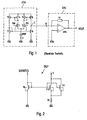
- Fig. 1 is a schematic circuit diagram of a CMOS (Complementary Metal Oxide Semiconductor) technology based Amplifier circuit shown.
- the amplifier circuit contains a transconductance amplifier OTA, which has a Input voltage VIN into a current 12 converts.
- the current I2 is powered by an operational amplifier OPA, which has a resistor R1 is connected as a current-to-voltage converter CVC, in converted an output voltage VOUT.
- OPA operational amplifier
- the transconductance amplifier OTA has in addition to high-impedance inputs 1 and 2, a high-impedance output 3.
- the transconductance amplifier OTA has a Differential amplifier stage, which a current source IREF and transistors T1 and T2. At the gate terminals the transistors T1 and T2 is the input voltage VIN. Furthermore, the transconductance amplifier OTA comprises three Current mirror, which with transistors T3 and T4, T5 and T6 or T7 and T8 are constructed.
- the transistors T1, T2, T7 and T8 are n-channel MOSFETs, while the transistors T3, T4, T5 and T6 are p-channel MOSFETs.
- VOUT R1 * I2 + VCM, where VCM indicates the center voltage.
- CMOS manufacturing processes become linear resistors often produced by deposition of polysilicon material.
- the temperature coefficient of such resistors, which the Resistance change with the temperature indicates is with the Resistance value per unit area of the polysilicon correlated. With only small resistance values per unit area the temperature coefficient is positive. The temperature coefficient decreases with increasing resistance per unit area and becomes negative for large resistances per unit area.
- the resistance R1 be high impedance. Otherwise, the steepness S of the Transconductance amplifier OTA be great, yet one to achieve acceptable gain of the amplifier circuit. But this would again be unacceptably large Power consumption of the transconductance amplifier OTA after itself pull.
- a high resistance R1 is used in CMOS technology Avoidance of excessive area consumption by polysilicon manufactured with a high resistance per unit area.
- the disadvantage of this is the resulting negative temperature coefficient of resistance R1.
- There the transconductance S of the transconductance amplifier OTA with increasing Temperature also decreases, is the gain factor the present amplifier circuit strongly dependent on temperature. This feature of the amplifier circuit is special disadvantageous if the amplifier circuit in a wide Temperature range is operated.
- manufacturing tolerances of the high resistance R1 influence.
- the present amplifier circuit is also used Amplify AC voltages.
- the idling frequency of Amplifier circuit also depends on the amplification factor from. For an unstable over a certain temperature range Gain factor leads to stability problems the amplifier circuit.
- the object of the invention is therefore an amplifier circuit to create which over a wide temperature range having temperature stabilized gain factor.
- the Temperature stability of the gain factor is intended in particular even when using high-impedance resistors with large ones Be ensured temperature coefficient.
- the amplifier circuit according to the invention becomes an input voltage by means of an overall gain factor into one Converted output voltage.
- the overall gain factor is a product of a first gain and a second gain factor.
- the amplifier circuit comprises first means for generating an intermediate signal in the form an intermediate current of the input voltage and the first Serve amplification factor. Furthermore, the amplifier circuit comprises second means by which the output voltage generated from the intermediate signal and the second gain factor become.
- the first means include a power source and a Transconductance amplifier, at whose input the input voltage is present and at the output of the intermediate current can be decoupled.
- the transconductance amplifier includes one operated below the threshold voltage and over the source terminal of the power source powered signal amplifying MOS transistor. In this case, that of the power source provided electricity and of which also depends the first Gain factor over the second gain factor an opposite temperature dependence.
- the advantage of the amplifier circuit according to the invention is justified on the opposite temperature dependencies of the first and second amplification factors. At a temperature change increases one of the two gain factors and the other gain factor drops, so overall a substantially temperature independent product of both gain factors and thus a temperature stabilized Overall gain factor.
- the amplifier circuit according to the invention becomes a compensation of the temperature dependencies of the two Gains achieved, resulting in a temperature independence of the overall gain over a wide range Temperature range results. Furthermore, a temperature-dependent variation of the transmission frequency suppresses the amplifier circuit according to the invention.
- the second means a current-voltage converter, which an operational amplifier and one in the feedback branch having the operational amplifier switched converter resistor.
- the current-voltage converter is used to convert the from the transconductance amplifier generated intermediate current in the output voltage.
- a particularly advantageous embodiment of the invention characterized in that provided by the power source Current and the transducer resistance opposite temperature dependencies exhibit.
- the temperature dependence of current supplied by the power source is transmitted on the temperature dependence of the transconductance of the transconductance amplifier. According to equation (3) results from the above claim a temperature-stabilized total gain factor the amplifier circuit.
- the Power source includes a power source bank whose input transistor with a temperature-stabilized input current is fed and the at least two parallel Having output transistors.
- the through the drain-source routes the output transistors generated output currents flow through at least one resistor and dine together the differential amplifier of the transconductance amplifier.
- the parallel connection of the at least two output transistors is the gate-source voltage of at least two Output transistors lower than the gate-source voltage of the input transistor.
- the due to the different Gate-source voltages generated voltage difference falls over the at least one resistance.
- the current passing through the drain-source paths of at least two output transistors are generated together and the differential amplifier of the transconductance amplifier is in its temperature dependence on the temperature dependence determines the at least one resistance, and indeed the temperature dependence of this behaves Current counter to the temperature dependence of at least a resistance. This also affects the temperature dependence the intermediate flow in opposite to the at least a resistance and thus also in opposite directions the transducer resistance, giving a temperature-stabilized overall gain entails.
- the input transistor and the at least two output transistors are well coordinated with each other, thereby also voltage variations caused by manufacturing tolerances Fixed.
- a temperature-stabilized input current can be, for example through a BGR (Band Gap Reference) circuit especially easy to generate.
- BGR Band Gap Reference
- the amplifier circuit according to the invention is particularly suitable for this purpose suitable to be integrated on a common substrate and in particular to be manufactured by means of CMOS technology.
- CMOS technology complementary metal-oxide-semiconductor
- both the transducer resistance as well as the at least one resistor the power source by deposition of polysilicon material generated with a high resistance per unit area become.
- This will be a low power consumption of Transconductance amplifier and a good temperature stability ensured the overall gain.
- the two linear resistors comparable (negative) temperature coefficients and manufacturing tolerances on.
- the inventive method serves to reinforce a Input voltage into an output voltage.
- the overall gain factor is which is the gain of the input voltage in the output voltage indicates a product of a first and a second gain factor
- first an intermediate signal in the form of an intermediate current from the input voltage and the first amplification factor happens by means of a current source and a transconductance amplifier, at whose inputs the input voltage is applied and at whose output an intermediate current can be coupled out.
- the first gain factor have opposite temperature dependencies versus the second gain factor on.
- a powered via the source terminal of the power source MOS transistor of the transconductance amplifier thereby operated below the threshold voltage.
- the generation of the output voltage takes place from the intermediate signal and the second gain factor.
- the advantage of the method according to the invention is again in the opposite temperature dependencies of the first and second gain factor. This compensation effect will, as already described, by the operation of the MOS transistor below the threshold voltage allows. from that Overall results over a wide operating temperature range stabilized total gain.
- Fig. 2 shows a schematic circuit diagram of an embodiment a current source IREF according to the invention, the Provision of a current 11 is used, which for the in Fig. 1 shown differential amplifier stage of the transconductance amplifier OTA is used.
- the current source IREF contains a Transistor T9, whose source-drain path between a Power source ICONST and a common fixed potential, in particular a mass VSS, is switched.
- the transistor T9 is as an input transistor of a power source bank with transistors T10 and T11 as output transistors via their gate terminals connected. Furthermore, the drain connection of the transistor T9 connected to its gate terminal.
- the Transistors T10 and T11 are at their drain and source terminals, respectively each connected to each other.
- the transistors T9, T10 and T11 are for example n-channel MOSFETs.
- the power source ICONST provides a temperature independent current. This requirement is fulfilled for example by a BGR circuit.
- the current generated by the power source ICONST is from the transistor T9 in the drain-source paths of the transistors T10 and T11 mirrored.
- the gate-source voltage of the transistor T9 is larger as the gate-source voltages of the transistors T10 and T11.
- the difference of these gate-source voltages falls above the Resistor R2 off.
- the bigger is also the Temperature dependence of the current 11 from the resistor R2, since the current 11 is a function of 1 / R2.
- the transconductance of a CMOS transistor is proportional to the one flowing through its drain-source path Current, provided the CMOS transistor below the threshold voltage is operated. Because the optimal working point for the CMOS transistors T1 and T2 having differential amplifier stage between the sub-threshold voltage range and the voltage range with slight inversion is the transconductance S of the transconductance amplifier OTA as well proportional to the current I1 and according to the preceding paragraph thus a function of 1 / R2. It follows that the Amplification factor of the amplifier circuit shown in FIG with the present invention current source IREF proportional to the resistance R1 and indirectly proportional to the resistor R2. Because the resistors R1 and R2 due have the same temperature dependencies in their design, is the gain over a wide temperature range independent of temperature.
Landscapes
- Engineering & Computer Science (AREA)
- Power Engineering (AREA)
- Amplifiers (AREA)
Claims (8)
- Circuit amplificateur ayant un facteur global d'amplification stabilisé en température, qui indique l'amplification d'une tension (VIN) d'entrée en une tension (VOUT) de sortie et qui est un produit d'un premier facteur (S) d'amplification et d'un deuxième facteur (R1) d'amplification, le circuit amplificateur comprenant :des premiers moyens de production d'un signal intermédiaire sous la forme d'un courant (I2) intermédiaire à partir de la tension (VIN) d'entrée et du premier facteur (S) d'amplification, qui aune source (IREF) de courant, etun amplificateur (OTA) de transductance à l'entrée (1, 2) duquel s'applique la tension d'entrée et à la sortie (3) duquel peut sortir le courant (I2) intermédiaire, dans lequelun transistor (T1, T2) MOS de l'amplificateur de transconducteur, cet amplificateur étant alimenté par l'intermédiaire de la borne de source par la source (IREF) de courant et amplifiant le signal fonctionne en dessous de la tension de seuil, etdes deuxièmes moyens de production de la tension (VOUT) de sortie à partir du signal (I2) intermédiaire et du deuxième facteur (R1) d'amplification, et dans lequelle courant (I1) mis à disposition par la source (IREF) de courant et aussi le premier facteur (S) d'amplification qui en dépend ont des variations en fonction de la température qui sont opposées par rapport au deuxième facteur (R1) d'amplification.
- Circuit amplificateur suivant la revendication 1,
caractériséen ce que la source (IREF) de courant alimente un amplificateur différentiel de l'amplificateur (OTA) de transductance. - Circuit amplificateur suivant la revendication 1 ou 2,
caractériséen ce que les deuxièmes moyens comportent un amplificateur (OPA) opérationnel monté avec une résistance (R1) de convertisseur en convertisseur (CVC) courant-tension et transformant le courant (I2) intermédiaire en la tension (VOUT) de sortie. - Circuit amplificateur suivant la revendication 3,
caractériséen ce que le courant (12) mis à disposition par la source (IREF) de courant et la résistance (R1) de convertisseur ont des variations en fonction de la température qui sont opposées. - Circuit amplificateur suivant l'une ou plusieurs des revendications 2 à 4,
caractériséen ce que la source (IREF) de courant comprend une rampe de source de courant, dont un transistor (T9) d'entrée est alimenté en un courant (ICONST) d'entrée stabilisé en température et qui a comme transistors de sortie au moins deux transistors (T10, T11) montés en parallèles, les courants de sortie produits par les sections drain-source des transistors (T10, T11) de sortie passant par au moins une résistance (R2) et alimentant conjointement l'amplificateur différentiel de l'amplificateur (OTA) de transductance. - Circuit amplificateur suivant l'une ou plusieurs des revendications précédentes,
caractériséen ce que les premiers et les deuxièmes moyens sont intégrés à un substrat commun et le circuit amplificateur est notamment un circuit amplificateur CMOS. - Circuit amplificateur suivant l'une des revendications 5 et 6,
caractériséen ce que la résistance (R1) de convertisseur et la au moins une résistance (R2) de la source (IREF) de courant sont des résistances intégrées linéaires qui ont notamment un grand coefficient de température. - Procédé d'amplification d'une tension (VIN) d'entrée en une tension (VOUT) de sortie avec un facteur global d'amplification stabilisé en température, qui indique l'amplification de la tension (VIN) d'entrée en la tension (VOUT) de sortie et qui est un produit d'un premier facteur (S) d'amplification et d'un deuxième facteur (R1) d'amplification, en effectuant les stades suivants :(1) production d'un signal intermédiaire sous la forme d'un courant (12) intermédiaire à partir de la tension (VIN) d'entrée et du premier facteur (S) d'amplification au moyen d'une source (IREF) de courant et d'un amplificateur (OTA) de transductance aux entrées (1, 2) duquel est appliquée la tension (VIN) d'entrée et de la sortie (3) duquel sort le courant intermédiaire, le courant (I1) mis à disposition par la source (IREF) de courant et également le premier facteur (S) d'amplification qui en dépend ayant des variations en fonction de la température qui sont opposées par rapport au deuxième facteur (R1) d'amplification, et fonctionnement d'un transistor (T1, T2) MOS de l'amplificateur de transductance, transducteur qui est alimenté par l'intermédiaire de la borne de source par la source (IREF) de courant, en dessous de la tension de seuil; et(2) production de la tension (VOUT) de sortie à partir du signal (I2) intermédiaire et du deuxième facteur (R1) d'amplification.
Applications Claiming Priority (3)
| Application Number | Priority Date | Filing Date | Title |
|---|---|---|---|
| DE10147101 | 2001-09-25 | ||
| DE10147101A DE10147101A1 (de) | 2001-09-25 | 2001-09-25 | Temperaturstabilisierte Verstärkerschaltung |
| PCT/DE2002/002707 WO2003028207A1 (fr) | 2001-09-25 | 2002-07-23 | Circuit amplificateur thermostable |
Publications (2)
| Publication Number | Publication Date |
|---|---|
| EP1430596A1 EP1430596A1 (fr) | 2004-06-23 |
| EP1430596B1 true EP1430596B1 (fr) | 2005-01-05 |
Family
ID=7700137
Family Applications (1)
| Application Number | Title | Priority Date | Filing Date |
|---|---|---|---|
| EP02754418A Expired - Lifetime EP1430596B1 (fr) | 2001-09-25 | 2002-07-23 | Circuit amplificateur thermostable |
Country Status (4)
| Country | Link |
|---|---|
| US (1) | US7102443B2 (fr) |
| EP (1) | EP1430596B1 (fr) |
| DE (2) | DE10147101A1 (fr) |
| WO (1) | WO2003028207A1 (fr) |
Families Citing this family (1)
| Publication number | Priority date | Publication date | Assignee | Title |
|---|---|---|---|---|
| CN103729004B (zh) * | 2014-01-07 | 2016-06-01 | 上海华虹宏力半导体制造有限公司 | 一种偏置电流产生电路 |
Family Cites Families (10)
| Publication number | Priority date | Publication date | Assignee | Title |
|---|---|---|---|---|
| US4159450A (en) * | 1978-05-22 | 1979-06-26 | Rca Corporation | Complementary-FET driver circuitry for push-pull class B transistor amplifiers |
| JP2525346B2 (ja) * | 1983-10-27 | 1996-08-21 | 富士通株式会社 | 定電流源回路を有する差動増幅回路 |
| US5739681A (en) * | 1992-02-07 | 1998-04-14 | Crosspoint Solutions, Inc. | Voltage regulator with high gain cascode current mirror |
| EP0561099B1 (fr) * | 1992-03-20 | 1995-09-06 | STMicroelectronics S.r.l. | Circuit pour supprimer la dépendance de la température et des variables de production, de la transconductance d'un étage transconducteur différentiel |
| JPH07225622A (ja) * | 1994-02-10 | 1995-08-22 | Fujitsu Ltd | 電界効果トランジスタを用いた定電流回路 |
| US5805401A (en) * | 1995-08-30 | 1998-09-08 | Cherry Semiconductor Corporation | Undervoltage lockout circuit with sleep pin |
| US5812024A (en) * | 1997-01-30 | 1998-09-22 | Lucent Technologies Inc. | Stabilization of gain-bandwidth product in analog circuit devices |
| US6107887A (en) * | 1998-10-02 | 2000-08-22 | Micro Linear Corporation | Differential to single-ended video cable driver having BICMOS current-mode operational amplifier |
| EP0961409B1 (fr) | 1999-02-10 | 2001-09-26 | Agilent Technologies Inc. a Delaware Corporation | Compensation des erreurs temporelles générées par des désadaptations thermiques |
| FR2834087A1 (fr) * | 2001-12-20 | 2003-06-27 | Koninkl Philips Electronics Nv | Circuit a transconductance sensiblement constante |
-
2001
- 2001-09-25 DE DE10147101A patent/DE10147101A1/de not_active Ceased
-
2002
- 2002-07-23 DE DE50201969T patent/DE50201969D1/de not_active Expired - Lifetime
- 2002-07-23 WO PCT/DE2002/002707 patent/WO2003028207A1/fr not_active Ceased
- 2002-07-23 US US10/490,260 patent/US7102443B2/en not_active Expired - Lifetime
- 2002-07-23 EP EP02754418A patent/EP1430596B1/fr not_active Expired - Lifetime
Also Published As
| Publication number | Publication date |
|---|---|
| US20050052243A1 (en) | 2005-03-10 |
| WO2003028207A1 (fr) | 2003-04-03 |
| DE10147101A1 (de) | 2003-04-24 |
| US7102443B2 (en) | 2006-09-05 |
| EP1430596A1 (fr) | 2004-06-23 |
| DE50201969D1 (de) | 2005-02-10 |
Similar Documents
| Publication | Publication Date | Title |
|---|---|---|
| DE102009054113B4 (de) | Prozess-, Spannungs- und Temperaturregelung für Hochgeschwindigkeits-Verstärker mit festem Verstärkungsgrad sowie mit variabler Verstärkung und geringem Stromverbrauch auf der Basis von MOSFET-Widerständen | |
| DE69011756T2 (de) | Stromspiegelschaltung. | |
| EP0483537B1 (fr) | Circuit de source de courant | |
| DE19959180A1 (de) | Verstärker mit dynamischer Kompensation und zugehöriges Verfahren | |
| DE102004002007B4 (de) | Transistoranordnung mit Temperaturkompensation und Verfahren zur Temperaturkompensation | |
| DE112012000470T5 (de) | Vorrichtung und Verfahren zur Miller-Kompensation bei mehrstufigen Verstärkern | |
| WO2003047108A2 (fr) | Circuit oscillateur stabilise en temperature | |
| DE69125807T2 (de) | Verfahren und Vorrichtung für schnelle bi-CMOS-Differenzverstärker mit gesteuerter Ausgangsspannungshub | |
| DE69229731T2 (de) | Von dem Eingangssignal dynamisch gesteuerter Transkonduktanz-Differenzverstärker | |
| DE102004027298B4 (de) | Auf dem Chip ausgeführter Hochpassfilter mit großer Zeitkonstanten | |
| DE2855303A1 (de) | Linearer verstaerker | |
| DE68921136T2 (de) | Transistorverstärker für hohe Anstiegsgeschwindigkeiten und kapazitive Belastungen. | |
| DE10154170A1 (de) | Differentialverstärker konstanter Transkonduktanz | |
| DE69917822T2 (de) | Operationsverstärker | |
| DE10066032B4 (de) | Schaltungsanordnung zur Steuerung der Verstärkung einer Verstärkerschaltung | |
| DE3933986A1 (de) | Komplementaerer stromspiegel zur korrektur einer eingangsoffsetspannung eines "diamond-followers" bzw. einer eingangsstufe fuer einen breitbandverstaerker | |
| EP0763916B1 (fr) | Circuit de réception à impédance d'entrée constante | |
| DE3856194T2 (de) | Verstärkerschaltung und mit der Verstärkerschaltung versehene Wiedergabeanordnung | |
| DE10047620B4 (de) | Schaltung zum Erzeugen einer Referenzspannung auf einem Halbleiterchip | |
| DE19533768C1 (de) | Stromtreiberschaltung mit Querstromregelung | |
| DE69413235T2 (de) | In verschiedene Konfigurationen umschaltbarer Operationsverstärker | |
| EP1101279B1 (fr) | Etage de sortie d'amplificateur | |
| DE112005000994B4 (de) | Hochpassfilter, welcher isolierte Gate-Feldeffekttransistoren verwendet | |
| DE69423464T2 (de) | Puffer für Sensor | |
| DE69522196T2 (de) | Pufferschaltung und Vorspannungsschaltung |
Legal Events
| Date | Code | Title | Description |
|---|---|---|---|
| PUAI | Public reference made under article 153(3) epc to a published international application that has entered the european phase |
Free format text: ORIGINAL CODE: 0009012 |
|
| 17P | Request for examination filed |
Effective date: 20040325 |
|
| AK | Designated contracting states |
Kind code of ref document: A1 Designated state(s): DE FI FR GB IT SE |
|
| AX | Request for extension of the european patent |
Extension state: AL LT LV MK RO SI |
|
| GRAP | Despatch of communication of intention to grant a patent |
Free format text: ORIGINAL CODE: EPIDOSNIGR1 |
|
| RIN1 | Information on inventor provided before grant (corrected) |
Inventor name: MUELLAUER, MARKUS |
|
| GRAS | Grant fee paid |
Free format text: ORIGINAL CODE: EPIDOSNIGR3 |
|
| GRAA | (expected) grant |
Free format text: ORIGINAL CODE: 0009210 |
|
| AK | Designated contracting states |
Kind code of ref document: B1 Designated state(s): DE |
|
| RBV | Designated contracting states (corrected) |
Designated state(s): DE |
|
| REF | Corresponds to: |
Ref document number: 50201969 Country of ref document: DE Date of ref document: 20050210 Kind code of ref document: P |
|
| PLBE | No opposition filed within time limit |
Free format text: ORIGINAL CODE: 0009261 |
|
| STAA | Information on the status of an ep patent application or granted ep patent |
Free format text: STATUS: NO OPPOSITION FILED WITHIN TIME LIMIT |
|
| 26N | No opposition filed |
Effective date: 20051006 |
|
| PGFP | Annual fee paid to national office [announced via postgrant information from national office to epo] |
Ref country code: DE Payment date: 20200923 Year of fee payment: 19 |
|
| REG | Reference to a national code |
Ref country code: DE Ref legal event code: R119 Ref document number: 50201969 Country of ref document: DE |
|
| PG25 | Lapsed in a contracting state [announced via postgrant information from national office to epo] |
Ref country code: DE Free format text: LAPSE BECAUSE OF NON-PAYMENT OF DUE FEES Effective date: 20220201 |