EP1431834A1 - Lithographische Projektionsmaske, Verfahren zur Herstellung eines Artikels unter Verwendung derselben und dabei hergestellter Artikel - Google Patents
Lithographische Projektionsmaske, Verfahren zur Herstellung eines Artikels unter Verwendung derselben und dabei hergestellter Artikel Download PDFInfo
- Publication number
- EP1431834A1 EP1431834A1 EP03258011A EP03258011A EP1431834A1 EP 1431834 A1 EP1431834 A1 EP 1431834A1 EP 03258011 A EP03258011 A EP 03258011A EP 03258011 A EP03258011 A EP 03258011A EP 1431834 A1 EP1431834 A1 EP 1431834A1
- Authority
- EP
- European Patent Office
- Prior art keywords
- radiation
- mask
- pattern
- substrate
- device pattern
- Prior art date
- Legal status (The legal status is an assumption and is not a legal conclusion. Google has not performed a legal analysis and makes no representation as to the accuracy of the status listed.)
- Granted
Links
- 238000004519 manufacturing process Methods 0.000 title claims description 9
- 239000000758 substrate Substances 0.000 claims abstract description 42
- 238000000034 method Methods 0.000 claims abstract description 32
- 230000005855 radiation Effects 0.000 claims description 37
- 238000000059 patterning Methods 0.000 claims description 11
- 239000000463 material Substances 0.000 claims description 10
- 239000010410 layer Substances 0.000 description 15
- 238000011161 development Methods 0.000 description 4
- 238000005259 measurement Methods 0.000 description 4
- XUIMIQQOPSSXEZ-UHFFFAOYSA-N Silicon Chemical compound [Si] XUIMIQQOPSSXEZ-UHFFFAOYSA-N 0.000 description 2
- 238000003491 array Methods 0.000 description 2
- 238000012937 correction Methods 0.000 description 2
- 238000009826 distribution Methods 0.000 description 2
- 230000006870 function Effects 0.000 description 2
- 238000003384 imaging method Methods 0.000 description 2
- 238000001459 lithography Methods 0.000 description 2
- 239000011159 matrix material Substances 0.000 description 2
- 230000003287 optical effect Effects 0.000 description 2
- 230000010363 phase shift Effects 0.000 description 2
- 238000003908 quality control method Methods 0.000 description 2
- 229910052710 silicon Inorganic materials 0.000 description 2
- 239000010703 silicon Substances 0.000 description 2
- 230000002238 attenuated effect Effects 0.000 description 1
- 230000005540 biological transmission Effects 0.000 description 1
- 239000011248 coating agent Substances 0.000 description 1
- 238000000576 coating method Methods 0.000 description 1
- 230000003750 conditioning effect Effects 0.000 description 1
- 238000010276 construction Methods 0.000 description 1
- 230000002950 deficient Effects 0.000 description 1
- 238000013461 design Methods 0.000 description 1
- 238000001514 detection method Methods 0.000 description 1
- 238000006073 displacement reaction Methods 0.000 description 1
- 230000009977 dual effect Effects 0.000 description 1
- 230000005684 electric field Effects 0.000 description 1
- 230000005670 electromagnetic radiation Effects 0.000 description 1
- 238000010894 electron beam technology Methods 0.000 description 1
- 238000005530 etching Methods 0.000 description 1
- 238000005286 illumination Methods 0.000 description 1
- 238000007689 inspection Methods 0.000 description 1
- 238000005468 ion implantation Methods 0.000 description 1
- 238000010884 ion-beam technique Methods 0.000 description 1
- 239000002346 layers by function Substances 0.000 description 1
- 239000004973 liquid crystal related substance Substances 0.000 description 1
- 230000005381 magnetic domain Effects 0.000 description 1
- 230000015654 memory Effects 0.000 description 1
- QSHDDOUJBYECFT-UHFFFAOYSA-N mercury Chemical compound [Hg] QSHDDOUJBYECFT-UHFFFAOYSA-N 0.000 description 1
- 229910052753 mercury Inorganic materials 0.000 description 1
- 238000001465 metallisation Methods 0.000 description 1
- 230000003647 oxidation Effects 0.000 description 1
- 238000007254 oxidation reaction Methods 0.000 description 1
- 239000002245 particle Substances 0.000 description 1
- 238000005498 polishing Methods 0.000 description 1
- 230000037452 priming Effects 0.000 description 1
- 238000012545 processing Methods 0.000 description 1
- 239000004065 semiconductor Substances 0.000 description 1
- 238000007493 shaping process Methods 0.000 description 1
- 239000010409 thin film Substances 0.000 description 1
Images

Classifications
-
- G—PHYSICS
- G03—PHOTOGRAPHY; CINEMATOGRAPHY; ANALOGOUS TECHNIQUES USING WAVES OTHER THAN OPTICAL WAVES; ELECTROGRAPHY; HOLOGRAPHY
- G03F—PHOTOMECHANICAL PRODUCTION OF TEXTURED OR PATTERNED SURFACES, e.g. FOR PRINTING, FOR PROCESSING OF SEMICONDUCTOR DEVICES; MATERIALS THEREFOR; ORIGINALS THEREFOR; APPARATUS SPECIALLY ADAPTED THEREFOR
- G03F9/00—Registration or positioning of originals, masks, frames, photographic sheets or textured or patterned surfaces, e.g. automatically
- G03F9/70—Registration or positioning of originals, masks, frames, photographic sheets or textured or patterned surfaces, e.g. automatically for microlithography
- G03F9/7073—Alignment marks and their environment
- G03F9/7084—Position of mark on substrate, i.e. position in (x, y, z) of mark, e.g. buried or resist covered mark, mark on rearside, at the substrate edge, in the circuit area, latent image mark, marks in plural levels
-
- G—PHYSICS
- G03—PHOTOGRAPHY; CINEMATOGRAPHY; ANALOGOUS TECHNIQUES USING WAVES OTHER THAN OPTICAL WAVES; ELECTROGRAPHY; HOLOGRAPHY
- G03F—PHOTOMECHANICAL PRODUCTION OF TEXTURED OR PATTERNED SURFACES, e.g. FOR PRINTING, FOR PROCESSING OF SEMICONDUCTOR DEVICES; MATERIALS THEREFOR; ORIGINALS THEREFOR; APPARATUS SPECIALLY ADAPTED THEREFOR
- G03F9/00—Registration or positioning of originals, masks, frames, photographic sheets or textured or patterned surfaces, e.g. automatically
- G03F9/70—Registration or positioning of originals, masks, frames, photographic sheets or textured or patterned surfaces, e.g. automatically for microlithography
- G03F9/7073—Alignment marks and their environment
- G03F9/7076—Mark details, e.g. phase grating mark, temporary mark
Definitions
- the present invention relates to a device manufacturing method comprising the steps of: providing a substrate that is at least partly covered by a layer of radiation-sensitive material; providing a projection beam of radiation using a radiation system; providing at least one patterning means including a device pattern; using said at least one patterning means to endow the projection beam with said device pattern; projecting the patterned beam of radiation onto a plurality of target portions of the layer of radiation sensitive material.
- the present invention also relates to a device manufactured by the method and to a lithographic projection mask for endowing a beam of radiation with a device pattern.
- patterning means as here employed should be broadly interpreted as referring to means that can be used to endow an incoming radiation beam with a patterned cross-section, corresponding to a pattern that is to be created in a target portion of the substrate; the term “light valve” can also be used in this context.
- the said pattern will correspond to a particular functional layer in a device being created in the target portion, such as an integrated circuit or other device (see below). Examples of such patterning means include:
- Lithographic projection apparatus can be used, for example, in the manufacture of integrated circuits (ICs).
- the patterning means may generate a circuit pattern corresponding to an individual layer of the IC, and this pattern can be imaged onto a target portion (e.g. comprising one or more dies) on a substrate (silicon wafer) that has been coated with a layer of radiation-sensitive material (resist).
- a target portion e.g. comprising one or more dies
- a substrate silicon wafer
- a layer of radiation-sensitive material resist
- a single wafer will contain a whole network of adjacent target portions that are successively irradiated via the projection system, one at a time.
- employing patterning by a mask on a mask table a distinction can be made between two different types of machine.
- each target portion is irradiated by exposing the entire mask pattern onto the target portion in one go; such an apparatus is commonly referred to as a wafer stepper.
- a wafer stepper In an alternative apparatus ⁇ commonly referred to as a step-and-scan apparatus ⁇ each target portion is irradiated by progressively scanning the mask pattern under the projection beam in a given reference direction (the "scanning" direction) while synchronously scanning the substrate table parallel or anti-parallel to this direction; since, in general, the projection system will have a magnification factor M (generally ⁇ 1), the speed V at which the substrate table is scanned will be a factor M times that at which the mask table is scanned. More information with regard to lithographic devices as here described can be gleaned, for example, from US 6,046,792, incorporated herein by reference.
- a pattern (e.g. in a mask) is imaged onto a substrate that is at least partially covered by a layer of radiation-sensitive material (resist).
- the substrate Prior to this imaging step, the substrate may undergo various procedures, such as priming, resist coating and a soft bake. After exposure, the substrate may be subjected to other procedures, such as a post-exposure bake (PEB), development, a hard bake and measurement/inspection of the imaged features.
- PEB post-exposure bake
- This array of procedures is used as a basis to pattern an individual layer of a device, e.g. an IC.
- Such a patterned layer may then undergo various processes such as etching, ion-implantation (doping), metallization, oxidation, chemo-mechanical polishing, etc., all intended to finish off an individual layer. If several layers are required, then the whole procedure, or a variant thereof, will have to be repeated for each new layer. Eventually, an array of devices will be present on the substrate (wafer). These devices are then separated from one another by a technique such as dicing or sawing, whence the individual devices can be mounted on a carrier, connected to pins, etc.
- the projection system may hereinafter be referred to as the "lens"; however, this term should be broadly interpreted as encompassing various types of projection system, including refractive optics, reflective optics, and catadioptric systems, for example.
- the radiation system may also include components operating according to any of these design types for directing, shaping or controlling the projection beam of radiation, and such components may also be referred to below, collectively or singularly, as a "lens".
- the lithographic apparatus may be of a type having two or more substrate tables (and/or two or more mask tables). In such "multiple stage” devices the additional tables may be used in parallel, or preparatory steps may be carried out on one or more tables while one or more other tables are being used for exposures. Dual stage lithographic apparatus are described, for example, in US 5,969,441 and WO 98/40791, incorporated herein by reference.
- the radiation beam in a lithography apparatus is only large enough to expose small parts of the wafer at a time.
- Two methods are used to overcome this so that the whole of the wafer may be exposed.
- the first is the so called scan mode in which the mask and substrate are moved simultaneously so that a large portion of the substrate can be exposed.
- the second is step mode in which an entire mask image is projected in one go onto a target portion of the substrate and the substrate is then shifted so that a different portion can then be exposed to the radiation beam.
- the portions exposed on the substrate table can either be partially overlapping or be abutting. In both overlapping and abutting cases it is clearly desirable to have the portions as well aligned as possible to maximize use of space on the substrate and therefore maximize throughput.
- Some devices being manufactured cover several target portions and alignment of these target portions becomes critical to ensure correct functioning of the device. In this case the same or different masks may be used for adjacent target portions.
- Box-in-box or similar metrologies rely on a particular relative placement of 2 concentric boxes or similar features (sized between 5 ⁇ m - 100 ⁇ m) to determine registration errors. This is done by measuring the relative positions of the said features printed during different process steps. Similarly, this method can be used to measure relative placement/registration errors of adjacent dies or fields by overlapping them such that the necessary features have the correct relative placement that is needed for the measurement.
- the method can be used to measure alignment of abutted device patterns. As a consequence the accuracy of the placement error can be more accurately assessed. Also the invention can be used with overlapping device patterns.
- This system has the advantage at the determining step can be carried out in an existing lithographic projection apparatus which generally already comprises alignment systems to measure alignments of other components in the lithographic projection apparatus.
- the degree of alignment and necessary correction can be measured directly in the lithographic projection apparatus and the results can be fed back such that the next wafer is stepped differently to account for the measured misalignment and so that the efficiency with which corrections are made is increased.
- the method acts as a quality control step to ensure the device will function correctly. If misalignment is detected, the resist may be removed and the process carried out again until the correct alignment is achieved.
- a lithographic projection mask for endowing a beam of radiation with a pattern, said mask comprising a device pattern and characterized in that said device pattern has at least one reference mark within it.
- the terms "radiation” and “beam” are used to encompass all types of electromagnetic radiation, including ultraviolet radiation (e.g. with a wavelength of 365, 248, 193, 157 or 126 nm) and EUV (extreme ultra-violet radiation, e.g. having a wavelength in the range 5-20 nm), as well as particle beams, such as ion beams or electron beams.
- ultraviolet radiation e.g. with a wavelength of 365, 248, 193, 157 or 126 nm
- EUV extreme ultra-violet radiation, e.g. having a wavelength in the range 5-20 nm
- particle beams such as ion beams or electron beams.
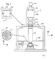
- Figure 1 schematically depicts a lithographic projection apparatus according to a particular embodiment of the invention.
- the apparatus comprises:
- the source LA (e.g. an Hg lamp) produces a beam of radiation.
- This beam is fed into an illumination system (illuminator) IL, either directly or after having traversed conditioning means, such as a beam expander Ex, for example.
- the illuminator IL may comprise adjusting means AM for setting the outer and/or inner radial extent (commonly referred to as ⁇ -outer and ⁇ -inner, respectively) of the intensity distribution in the beam.
- ⁇ -outer and ⁇ -inner commonly referred to as ⁇ -outer and ⁇ -inner, respectively
- it will generally comprise various other components, such as an integrator IN and a condenser CO.
- the beam PB impinging on the mask MA has a desired uniformity and intensity distribution in its cross-section.
- the source LA may be within the housing of the lithographic projection apparatus (as is often the case when the source LA is a mercury lamp, for example), but that it may also be remote from the lithographic projection apparatus, the radiation beam which it produces being led into the apparatus (e.g. with the aid of suitable directing mirrors); this latter scenario is often the case when the source LA is an excimer laser.
- the current invention and Claims encompass both of these scenarios.
- the beam PB subsequently intercepts the mask MA, which is held on a mask table MT. Having been selectively reflected by the mask MA, the beam PB passes through the lens PL, which focuses the beam PB onto a target portion C of the substrate W. With the aid of the second positioning means (and interferometric measuring means IF), the substrate table WT can be moved accurately, e.g. so as to position different target portions C in the path of the beam PB. Similarly, the first positioning means can be used to accurately position the mask MA with respect to the path of the beam PB, e.g. after mechanical retrieval of the mask MA from a mask library, or during a scan.
- the mask table MT may just be connected to a short stroke actuator, or may be fixed.
- the depicted apparatus can be used in two different modes:
- This invention is primarily concerned with the step mode in which a plurality of target portions C on the substrate W are exposed in sequence.
- the target portions are aligned so that they either abut or so that they overlap by small amounts (so called pattern stitching). This sort of process can only be effective if the target portions C are accurately positioned relative to one another.
- the present invention is directed to a method of determining the alignments of neighbouring target portions so that the step mode can be optimized.
- the mask MA has a device pattern DP on it (see Figure 2 in which the details of the device are not illustrated) which is intended to be projected onto the target portions C of the substrate W.
- the device pattern DP of the mask MA comprises at least one reference mark 5 which is projected but which does not form a working part of the final manufactured device.
- the reference mark 5 is used to determine the relative placement of target portions C as described below.
- the reference mark 5 is within the device pattern, that is, parts of the device pattern of the mask completely surround the reference mark on all sides of the reference mark 5 and the reference mark 5 is not merely at the edge of the device pattern.
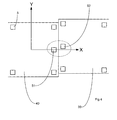
- a plurality of patterns corresponding to the device pattern DP of the mask MA shown in Figure 2 are first projected onto a target portion C on a radiation sensitive material on a surface of the substrate which is then developed to form a plurality of developed patterns 10, 20, 30, 40, 50.
- These patterns 10, 20, 30, 40, 50 may either abut as illustrated or may overlap slightly as described above.
- the relative alignment of the patterns in the XY directions in the plane of the surface of the substrate can be determined by measuring alignment of the at least one reference mark 5, 51, 52 of respective developed patterns 10, 20, 30, 40, 50.
- the adjacent development patterns 10, 20, 30, 40, 50 need not be of the same type, especially if a single device to be manufactured extends over several target portions. In this case different masks having different device patterns DP will be used but adjacent device patterns will need to include compatably placed alignment marks 5.
- the alignment marks 5 are completely within the development patterns 10, 20, 30, 40, 50.
- Figure 4 shows in detail the measurement of misalignment of two adjacent developed patterns 30, 40 by determination of the relative positions of reference marks 51 and 52. This may be carried out before or after development of the pattern.
- the error in positioning of the substrate table during the step mode can be calculated and the process for manufacturing the following substrate, especially the movement of the substrate W during stepping, can be optimized on this information.
- the method can be used as a quality control method when the device to be manufactured extends across several target portions. In this case if a degree of misalignment is detected which would result in a defective device, the layer of exposed radiation-sensitive material can be removed and the process for that layer can be carried out again. In this way, the effort expended in previously deposited layers need not be disguarded and no effort need be expended in subsequent layers when the device would in any case not function due to the misalignment.
- the at least one reference mark 5, 51, 52 of adjacent developed patterns are positioned close to one another. This is achieved by having at least one of the at least one reference mark 5, 51, 52 associated with each edge of the device pattern DP which will, once projected and developed, abut against another edge of the device pattern DP. This may be achieved by providing the device pattern DP with at least two axes of symmetry as regards the reference mark 5. This is illustrated in Figure 2 where it can be seen that at least two such axes 80, 85 exist. If the device pattern DP is rectanglar, it is convenient to position a reference mark 5 midway along each edge and spaced away from the edge though the mark may be positioned anywhere. Of course the reference mark 5 should be positioned in an area of the device pattern DP that contains no actual device details.
- Lithographic projection machines already comprise alignment sensors for precise positioning of various devices such as the mask MA using positioning marks M1, M2 and the substrate W using alignment marks P1, P2. These alignment systems are based on optical defraction methods using defraction gratings.
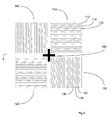
- Figure 5 shows a reference mark 5 which may be used in the device pattern DP in the present invention.
- Existing alignment systems in a lithographic projection apparatus can use such marks 5 to measure relative displacement of developed patterns 10, 20, 30, 40, 50.
- This pattern of alignment mark is known and it has been explained in detail in WO 98/39689 hereinby incorporated by reference and which document also explains on-axis and off-axis alignment using such marks.
Landscapes
- Physics & Mathematics (AREA)
- General Physics & Mathematics (AREA)
- Exposure And Positioning Against Photoresist Photosensitive Materials (AREA)
Priority Applications (1)
| Application Number | Priority Date | Filing Date | Title |
|---|---|---|---|
| EP03258011A EP1431834B1 (de) | 2002-12-19 | 2003-12-18 | Verfahren zur Herstellung eines Artikels unter Verwendung einer lithographischen Projektionsmaske |
Applications Claiming Priority (3)
| Application Number | Priority Date | Filing Date | Title |
|---|---|---|---|
| EP02258762 | 2002-12-19 | ||
| EP02258762 | 2002-12-19 | ||
| EP03258011A EP1431834B1 (de) | 2002-12-19 | 2003-12-18 | Verfahren zur Herstellung eines Artikels unter Verwendung einer lithographischen Projektionsmaske |
Publications (2)
| Publication Number | Publication Date |
|---|---|
| EP1431834A1 true EP1431834A1 (de) | 2004-06-23 |
| EP1431834B1 EP1431834B1 (de) | 2008-07-23 |
Family
ID=32395463
Family Applications (1)
| Application Number | Title | Priority Date | Filing Date |
|---|---|---|---|
| EP03258011A Expired - Lifetime EP1431834B1 (de) | 2002-12-19 | 2003-12-18 | Verfahren zur Herstellung eines Artikels unter Verwendung einer lithographischen Projektionsmaske |
Country Status (1)
| Country | Link |
|---|---|
| EP (1) | EP1431834B1 (de) |
Cited By (1)
| Publication number | Priority date | Publication date | Assignee | Title |
|---|---|---|---|---|
| TWI608307B (zh) * | 2015-02-26 | 2017-12-11 | 上海微電子裝備(集團)股份有限公司 | Mask board transmission device and transmission method |
Citations (5)
| Publication number | Priority date | Publication date | Assignee | Title |
|---|---|---|---|---|
| US4657379A (en) * | 1984-05-11 | 1987-04-14 | Nippon Kogaku K. K. | Photomask and exposure apparatus using the same |
| EP0466335A2 (de) * | 1990-06-12 | 1992-01-15 | Nec Corporation | Verfahren zur Herstellung von Halbleiteranordnungen |
| US5440138A (en) * | 1993-01-06 | 1995-08-08 | Nikon Corporation | Exposure method |
| US5715063A (en) * | 1995-05-24 | 1998-02-03 | Nikon Corporation | Projection exposure method |
| JP2002134397A (ja) * | 2000-10-25 | 2002-05-10 | Sony Corp | フォトマスク、半導体装置、半導体チップパターンの露光方法、チップアライメント精度検査装置 |
Family Cites Families (2)
| Publication number | Priority date | Publication date | Assignee | Title |
|---|---|---|---|---|
| JPS61201427A (ja) * | 1985-03-04 | 1986-09-06 | Nippon Kogaku Kk <Nikon> | 位置ずれ検出方法 |
| JP3643572B2 (ja) * | 2002-05-31 | 2005-04-27 | 株式会社アドテックエンジニアリング | 投影露光装置及び位置合わせ装置 |
-
2003
- 2003-12-18 EP EP03258011A patent/EP1431834B1/de not_active Expired - Lifetime
Patent Citations (5)
| Publication number | Priority date | Publication date | Assignee | Title |
|---|---|---|---|---|
| US4657379A (en) * | 1984-05-11 | 1987-04-14 | Nippon Kogaku K. K. | Photomask and exposure apparatus using the same |
| EP0466335A2 (de) * | 1990-06-12 | 1992-01-15 | Nec Corporation | Verfahren zur Herstellung von Halbleiteranordnungen |
| US5440138A (en) * | 1993-01-06 | 1995-08-08 | Nikon Corporation | Exposure method |
| US5715063A (en) * | 1995-05-24 | 1998-02-03 | Nikon Corporation | Projection exposure method |
| JP2002134397A (ja) * | 2000-10-25 | 2002-05-10 | Sony Corp | フォトマスク、半導体装置、半導体チップパターンの露光方法、チップアライメント精度検査装置 |
Non-Patent Citations (1)
| Title |
|---|
| PATENT ABSTRACTS OF JAPAN vol. 2002, no. 09 4 September 2002 (2002-09-04) * |
Cited By (1)
| Publication number | Priority date | Publication date | Assignee | Title |
|---|---|---|---|---|
| TWI608307B (zh) * | 2015-02-26 | 2017-12-11 | 上海微電子裝備(集團)股份有限公司 | Mask board transmission device and transmission method |
Also Published As
| Publication number | Publication date |
|---|---|
| EP1431834B1 (de) | 2008-07-23 |
Similar Documents
| Publication | Publication Date | Title |
|---|---|---|
| US7560196B2 (en) | Mask for exposing an alignment mark, and method and computer program for designing the mask | |
| US7466413B2 (en) | Marker structure, mask pattern, alignment method and lithographic method and apparatus | |
| US6710849B2 (en) | Method for calibrating a lithographic projection apparatus and apparatus capable of applying such a method | |
| US7019814B2 (en) | Lithographic projection mask, device manufacturing method, and device manufactured thereby | |
| EP1477851A1 (de) | Verfahren zur Herstellung einer Vorrichtung und lithographischer Apparat | |
| US20060092419A1 (en) | Optical position assessment apparatus and method | |
| EP1406126A1 (de) | Verfahren zur Herstellung einer Vorrichtung | |
| EP1353229A1 (de) | Lithographischer Apparat, Verfahren zur Herstellung eines Artikels und dabei hergesteller Artikel | |
| US6906785B2 (en) | Lithographic apparatus, device manufacturing method, and device manufactured thereby | |
| EP1477861A1 (de) | Verfahren zur Eichung eines lithographischen Geräts, Ausrichtverfahren, Komputerprogramm, lithographisches Gerät und Verfahren zur Herstellung einer Vorrichtung | |
| US6937318B2 (en) | Lithographic apparatus, computer program, device manufacturing method, and device manufactured thereby | |
| US6955074B2 (en) | Lithographic apparatus, method of calibration, calibration plate, device manufacturing method, and device manufactured thereby | |
| US6914664B2 (en) | Lithographic apparatus, alignment method and device manufacturing method | |
| US20030213921A1 (en) | Device manufacturing method, device manufactured thereby and computer programs | |
| EP1394616A1 (de) | Ausrichtgerät, lithographischer Apparat, Ausrichtungsverfahren und Verfahren zur Herstellung einer Vorrichtung | |
| EP1260870A1 (de) | Ausrichtmarke | |
| EP1186959B1 (de) | Verfahren zur Eichung eines lithographischen Projektionsapparats | |
| EP1431834B1 (de) | Verfahren zur Herstellung eines Artikels unter Verwendung einer lithographischen Projektionsmaske | |
| US7041996B2 (en) | Method of aligning a substrate, a computer program, a device manufacturing method and a device manufactured thereby | |
| EP2204697A2 (de) | Markerstruktur, lithographische Projektionsvorrichtung, Verfahren zur Substratausrichtung mittels solch einer Struktur und Substrat mit solch einer Markerstruktur | |
| EP1357435A1 (de) | Lithographischer Apparat und Verfahren zur Herstellung einer Vorrichtung | |
| EP1260869A1 (de) | Substrat mit Ausrichtungsmarke in einer wesentlich transparenten Prozessschicht | |
| EP1338924B1 (de) | Verfahren zur Ausrichtung und Verfahren zur Herstellung eines Artikels | |
| EP1353234A1 (de) | Verfahren zur Herstellung einer Vorrichtung, diese Vorrichtung und Rechnerprogramm | |
| EP1398670A2 (de) | Methode zum Ausrichten eines Substrates, ein Computerprogramm und ein Verfahren zur Herstellung eines Artikels |
Legal Events
| Date | Code | Title | Description |
|---|---|---|---|
| PUAI | Public reference made under article 153(3) epc to a published international application that has entered the european phase |
Free format text: ORIGINAL CODE: 0009012 |
|
| AK | Designated contracting states |
Kind code of ref document: A1 Designated state(s): AT BE BG CH CY CZ DE DK EE ES FI FR GB GR HU IE IT LI LU MC NL PT RO SE SI SK TR |
|
| AX | Request for extension of the european patent |
Extension state: AL LT LV MK |
|
| 17P | Request for examination filed |
Effective date: 20040715 |
|
| RAP1 | Party data changed (applicant data changed or rights of an application transferred) |
Owner name: ASML NETHERLANDS B.V. |
|
| 17Q | First examination report despatched |
Effective date: 20040922 |
|
| AKX | Designation fees paid |
Designated state(s): DE FR GB IT NL |
|
| GRAP | Despatch of communication of intention to grant a patent |
Free format text: ORIGINAL CODE: EPIDOSNIGR1 |
|
| RTI1 | Title (correction) |
Free format text: A DEVICE MANUFACTURING METHOD USING A LITHOGRAPHIC PROJECTION MASK |
|
| GRAS | Grant fee paid |
Free format text: ORIGINAL CODE: EPIDOSNIGR3 |
|
| GRAA | (expected) grant |
Free format text: ORIGINAL CODE: 0009210 |
|
| AK | Designated contracting states |
Kind code of ref document: B1 Designated state(s): DE FR GB IT NL |
|
| REG | Reference to a national code |
Ref country code: GB Ref legal event code: FG4D |
|
| REF | Corresponds to: |
Ref document number: 60322331 Country of ref document: DE Date of ref document: 20080904 Kind code of ref document: P |
|
| NLV1 | Nl: lapsed or annulled due to failure to fulfill the requirements of art. 29p and 29m of the patents act | ||
| PG25 | Lapsed in a contracting state [announced via postgrant information from national office to epo] |
Ref country code: NL Free format text: LAPSE BECAUSE OF FAILURE TO SUBMIT A TRANSLATION OF THE DESCRIPTION OR TO PAY THE FEE WITHIN THE PRESCRIBED TIME-LIMIT Effective date: 20080723 |
|
| PGFP | Annual fee paid to national office [announced via postgrant information from national office to epo] |
Ref country code: FR Payment date: 20081212 Year of fee payment: 6 |
|
| PGFP | Annual fee paid to national office [announced via postgrant information from national office to epo] |
Ref country code: DE Payment date: 20081219 Year of fee payment: 6 |
|
| PLBE | No opposition filed within time limit |
Free format text: ORIGINAL CODE: 0009261 |
|
| STAA | Information on the status of an ep patent application or granted ep patent |
Free format text: STATUS: NO OPPOSITION FILED WITHIN TIME LIMIT |
|
| 26N | No opposition filed |
Effective date: 20090424 |
|
| GBPC | Gb: european patent ceased through non-payment of renewal fee |
Effective date: 20081218 |
|
| PG25 | Lapsed in a contracting state [announced via postgrant information from national office to epo] |
Ref country code: IT Free format text: LAPSE BECAUSE OF FAILURE TO SUBMIT A TRANSLATION OF THE DESCRIPTION OR TO PAY THE FEE WITHIN THE PRESCRIBED TIME-LIMIT Effective date: 20080723 |
|
| PG25 | Lapsed in a contracting state [announced via postgrant information from national office to epo] |
Ref country code: GB Free format text: LAPSE BECAUSE OF NON-PAYMENT OF DUE FEES Effective date: 20081218 |
|
| REG | Reference to a national code |
Ref country code: FR Ref legal event code: ST Effective date: 20100831 |
|
| PG25 | Lapsed in a contracting state [announced via postgrant information from national office to epo] |
Ref country code: FR Free format text: LAPSE BECAUSE OF NON-PAYMENT OF DUE FEES Effective date: 20091231 |
|
| PG25 | Lapsed in a contracting state [announced via postgrant information from national office to epo] |
Ref country code: DE Free format text: LAPSE BECAUSE OF NON-PAYMENT OF DUE FEES Effective date: 20100701 |