EP1432037A2 - Integriertes Bauelement mit Schottky-diode und mit MOS Transistor und zugehöriges Herstellungsverfahren - Google Patents
Integriertes Bauelement mit Schottky-diode und mit MOS Transistor und zugehöriges Herstellungsverfahren Download PDFInfo
- Publication number
- EP1432037A2 EP1432037A2 EP03079092A EP03079092A EP1432037A2 EP 1432037 A2 EP1432037 A2 EP 1432037A2 EP 03079092 A EP03079092 A EP 03079092A EP 03079092 A EP03079092 A EP 03079092A EP 1432037 A2 EP1432037 A2 EP 1432037A2
- Authority
- EP
- European Patent Office
- Prior art keywords
- layer
- conductivity type
- substrate
- stripes
- elementary
- Prior art date
- Legal status (The legal status is an assumption and is not a legal conclusion. Google has not performed a legal analysis and makes no representation as to the accuracy of the status listed.)
- Granted
Links
Images


Classifications
-
- H—ELECTRICITY
- H10—SEMICONDUCTOR DEVICES; ELECTRIC SOLID-STATE DEVICES NOT OTHERWISE PROVIDED FOR
- H10D—INORGANIC ELECTRIC SEMICONDUCTOR DEVICES
- H10D30/00—Field-effect transistors [FET]
- H10D30/01—Manufacture or treatment
- H10D30/021—Manufacture or treatment of FETs having insulated gates [IGFET]
- H10D30/028—Manufacture or treatment of FETs having insulated gates [IGFET] of double-diffused metal oxide semiconductor [DMOS] FETs
- H10D30/0291—Manufacture or treatment of FETs having insulated gates [IGFET] of double-diffused metal oxide semiconductor [DMOS] FETs of vertical DMOS [VDMOS] FETs
-
- H—ELECTRICITY
- H10—SEMICONDUCTOR DEVICES; ELECTRIC SOLID-STATE DEVICES NOT OTHERWISE PROVIDED FOR
- H10D—INORGANIC ELECTRIC SEMICONDUCTOR DEVICES
- H10D62/00—Semiconductor bodies, or regions thereof, of devices having potential barriers
- H10D62/01—Manufacture or treatment
- H10D62/051—Forming charge compensation regions, e.g. superjunctions
-
- H—ELECTRICITY
- H10—SEMICONDUCTOR DEVICES; ELECTRIC SOLID-STATE DEVICES NOT OTHERWISE PROVIDED FOR
- H10D—INORGANIC ELECTRIC SEMICONDUCTOR DEVICES
- H10D62/00—Semiconductor bodies, or regions thereof, of devices having potential barriers
- H10D62/10—Shapes, relative sizes or dispositions of the regions of the semiconductor bodies; Shapes of the semiconductor bodies
- H10D62/102—Constructional design considerations for preventing surface leakage or controlling electric field concentration
- H10D62/103—Constructional design considerations for preventing surface leakage or controlling electric field concentration for increasing or controlling the breakdown voltage of reverse-biased devices
- H10D62/105—Constructional design considerations for preventing surface leakage or controlling electric field concentration for increasing or controlling the breakdown voltage of reverse-biased devices by having particular doping profiles, shapes or arrangements of PN junctions; by having supplementary regions, e.g. junction termination extension [JTE]
- H10D62/109—Reduced surface field [RESURF] PN junction structures
- H10D62/111—Multiple RESURF structures, e.g. double RESURF or 3D-RESURF structures
-
- H—ELECTRICITY
- H10—SEMICONDUCTOR DEVICES; ELECTRIC SOLID-STATE DEVICES NOT OTHERWISE PROVIDED FOR
- H10D—INORGANIC ELECTRIC SEMICONDUCTOR DEVICES
- H10D64/00—Electrodes of devices having potential barriers
- H10D64/20—Electrodes characterised by their shapes, relative sizes or dispositions
- H10D64/27—Electrodes not carrying the current to be rectified, amplified, oscillated or switched, e.g. gates
- H10D64/311—Gate electrodes for field-effect devices
- H10D64/411—Gate electrodes for field-effect devices for FETs
- H10D64/511—Gate electrodes for field-effect devices for FETs for IGFETs
- H10D64/517—Gate electrodes for field-effect devices for FETs for IGFETs characterised by the conducting layers
- H10D64/518—Gate electrodes for field-effect devices for FETs for IGFETs characterised by the conducting layers characterised by their lengths or sectional shapes
-
- H—ELECTRICITY
- H10—SEMICONDUCTOR DEVICES; ELECTRIC SOLID-STATE DEVICES NOT OTHERWISE PROVIDED FOR
- H10D—INORGANIC ELECTRIC SEMICONDUCTOR DEVICES
- H10D64/00—Electrodes of devices having potential barriers
- H10D64/20—Electrodes characterised by their shapes, relative sizes or dispositions
- H10D64/27—Electrodes not carrying the current to be rectified, amplified, oscillated or switched, e.g. gates
- H10D64/311—Gate electrodes for field-effect devices
- H10D64/411—Gate electrodes for field-effect devices for FETs
- H10D64/511—Gate electrodes for field-effect devices for FETs for IGFETs
- H10D64/517—Gate electrodes for field-effect devices for FETs for IGFETs characterised by the conducting layers
- H10D64/519—Gate electrodes for field-effect devices for FETs for IGFETs characterised by the conducting layers characterised by their top-view geometrical layouts
-
- H—ELECTRICITY
- H10—SEMICONDUCTOR DEVICES; ELECTRIC SOLID-STATE DEVICES NOT OTHERWISE PROVIDED FOR
- H10D—INORGANIC ELECTRIC SEMICONDUCTOR DEVICES
- H10D84/00—Integrated devices formed in or on semiconductor substrates that comprise only semiconducting layers, e.g. on Si wafers or on GaAs-on-Si wafers
- H10D84/101—Integrated devices comprising main components and built-in components, e.g. IGBT having built-in freewheel diode
- H10D84/141—VDMOS having built-in components
- H10D84/146—VDMOS having built-in components the built-in components being Schottky barrier diodes
-
- H—ELECTRICITY
- H10—SEMICONDUCTOR DEVICES; ELECTRIC SOLID-STATE DEVICES NOT OTHERWISE PROVIDED FOR
- H10D—INORGANIC ELECTRIC SEMICONDUCTOR DEVICES
- H10D62/00—Semiconductor bodies, or regions thereof, of devices having potential barriers
- H10D62/10—Shapes, relative sizes or dispositions of the regions of the semiconductor bodies; Shapes of the semiconductor bodies
- H10D62/17—Semiconductor regions connected to electrodes not carrying current to be rectified, amplified or switched, e.g. channel regions
- H10D62/393—Body regions of DMOS transistors or IGBTs
Definitions
- the present invention refers to an integrated device with Schottky diode and with MOS transistor and to the related manufacturing process.
- the MOS devices are frequently used as synchronous rectifiers, for example in the bridge circuit configurations of the DC/DC converters.
- a synchronous rectifier acts like a diode: it is turned on when its equivalent diode has to conduct and it is turned off when the equivalent diode has to cease the conduction.
- the vertical semiconductor MOS devices have an intrinsic diode, which is formed by the junction between the body region and the drain region and which is called "body diode", that interferes with the operation of the MOS device as a synchronous rectifier. In fact such body diode switches slowly, it has a high conduction voltage and may product electromagnetic radiation emissions in the circuit configurations where the MOS device is inserted.
- Another solution used for reducing the switching time of the body diode consists of arranging a Schottky diode, which has equal voltage and a suitable area, in parallel thereto.
- the Schottky diode has a fast recovery because minority carriers do not exist and has lower conduction voltage values for the different barrier heights.
- the combination of the body diode in parallel to the Schottky diode provides for an equivalent structure having a short switching time and a lower conduction voltage.
- Discrete component structures are used for the structure made up by the body diode in parallel to the Schottky diode.
- FIG. 1 An integrated type structure is disclosed in US 5886383.
- FIG. 1 A MOS device having a polygonal cell structure is formed together with a Schottky diode in a common silicon substrate of N+-type.
- a N-type epitaxial layer 100 is formed on the said silicon substrate which receives a plurality of P-type regions 41 and 42 which comprise source regions 140 and 150 and which have central openings 44 and 45 through which the region 100 protrudes, so that a metal layer 220 contacts the region 100; in such a way the diode Schottky is formed.
- each channel region is covered by a gate oxide on which a polysilicon layer 200 is superimposed.
- Another oxide layer 210 is superimposed on the polysilicon layer for insulating it from the metal layer 220.
- a drain electrode is applied under the chip 90.
- the Schottky diode in the MOS device in Figure 1 is formed by interrupting the body regions of the single elementary cells of the device, by forming an alternation of body regions and device substrate portions; said substrate portions are contacted by the metal used for contacting the source regions.
- this object is obtained by means of an integrated device comprising a MOS transistor and a Schottky diode which are formed on a semiconductor substrate of a first conductivity type, said device comprising a plurality of body region stripes of a second conductivity type which are adjacent and parallel to each other, a first metal layer placed over said substrate and a second metal layer placed under said substrate, said device comprising a plurality of elementary structures parallel to each other each one of which comprises first zones provided with a silicon oxide layer placed over a portion of said substrate which is comprised between two adjacent body region stripes, a polysilicon layer superimposed to said silicon oxide layer, a dielectric layer placed over and around the polysilicon layer, some stripes of said plurality of adjacent body region stripes comprising source regions of the first conductivity type which are placed adj acent to said first zones of the elementary structures to form elementary cells of said MOS transistor, said elementary structures and said body regions stripes extending longitudinally in a transversal way to the formation of the channel in said elementary cells of the MOS transistor,
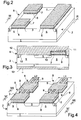
- an integrated device according to a first embodiment of the invention is shown; said integrated device has a stripe structure.
- An N-type epitaxial layer 2 with low dopant concentration is grown on a N-type substrate 1 with high dopant concentration.
- a plurality of body region stripes 3 having P-type dopant are formed inside the epitaxial layer 2.
- the body region stripes 3 are adjacent and parallel to each other and they are alternated with portions 5 of the epitaxial layer 2, as shown in Figure 2.
- a silicon oxide layer 6 is placed and a polysilicon layer 7 is placed over the silicon oxide layer 6 ( Figures 2 and 3); the layers 6 and 7 have a stripe shape and the stripes are parallel to each other and form a plurality of elementary structure of the integrated device.
- the succession of the steps of the integrated device manufacturing process continues with a successive masking and attack step of the polysilicon 7 and of the silicon oxide 6 of at least one elementary structure, that is of at least one polysilicon stripe 7 and of the underlying silicon oxide layer 6, on at least one zone 8.
- the masking and the attack of the polysilicon 7 and of the silicon oxide 6 are made up for forming an interruption of the elementary structure, that is of the polysilicon stripe 7 and of the underlying silicon oxide stripe 6, for the entire width of the stripes.
- the regions 10 with high dopant concentration of N-type are formed and there is a step for the thermal diffusion of the P dopant of the body regions 3 so that they extend partially under the silicon oxide stripes 6 ( Figure 3).
- MOS elementary cells (wherein for MOS elementary cell it is intended the block constituted by two source regions 10, a portion 5 of the epitaxial layer 2 and a gate structure formed by the layers 6 and 7) are formed in the other zones which form the MOS power transistor.
- the metal layers 12 and 13 are respectively the source and drain electrodes of each MOS elementary cell.
- the formation of the channel of said MOS elementary cells occurs in a transversal way with respect to the longitudinal extension of the body stripes 3 and of the elementary structures formed by the stripes 6 and 7.
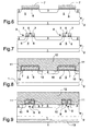
- FIGs 4, 6-9 an integrated device according to a second embodiment of the present invention is shown which differs from the first embodiment because the masking and attack step of the polysilicon 7 and of the silicon oxide 6 of at least one elementary structure, that is of at least one polysilicon stripe 7 and at least one silicon oxide stripe 6, in the zone 8 does not provide the whole removal of the oxide and of the polysilicon in said zone 8.
- an opening 9 for example comprised between 1 ⁇ m and 5 ⁇ m
- the dielectric layer 11 covers the walls of the opening 9 to prevent the contact of the metal 12 with the polysilicon 7.
- the width L2 of the stripes 6 and 7 in the zones 8 is preferably smaller than the typical width L1 of the stripes 6 and 7, as shown in Figure 4; it is defined in base on the breakdown voltage of the integrated device which is not lower than that of the integrated device without Schottky diodes, therefore the width L2 depends on the dopant concentration of the regions 3, on the thickness of the oxide, etc.
- zones 8 in more than one elementary structure are formed; said zones 8 are preferably aligned transversal to each other and are alternated longitudinally to the MOS elementary cells, as shown in Figure 4.
- the only difference consists in that the width L2 of the stripes 6 and 7 of the zones 8 is equal to the typical width L1 of the stripes 6 and 7.
- the integrated device is therefore formed by a MOS power transistor and by a Schottky diode arranged in parallel to the body diode.
- FIG. 10 A part of a multi-drain device according to prior art is shown in Figure 10.
- the integrated device in Figure 10 presents a multi-drain (MD) device structure, that is it presents a formation of P-type region columns under the body regions 300.
- a succession of N-type epitaxial layers 207 with low dopant concentration are formed on a N-type semiconductor substrate 101 with high dopant concentration.
- After the formation of the last epitaxial layer 207 of the succession of epitaxial layers 207 columns 227 of the P-type regions 217 are formed.
- a plurality of stripes of body regions 300 having P-type dopant is formed inside the last epitaxial layer 207; the body region stripes 300 are adjacent and parallel to each other and they are alternated to portions 500 of the last epitaxial layer 207, as shown in Figure 10.
- At least one source region 107 is inside each body stripes 300.
- a silicon oxide layer 60 is placed over the plurality of regions 500 of the last epitaxial layer 207 and a polysilicon layer 70 is placed over the silicon oxide layer 60; the layers 60 and 70 have shape of stripes which are parallel to each other and which form a plurality of elementary structure of the integrated device.
- a stripe shape dielectric layer 311 is placed over the polysilicon layers 70 and a metal layer 80 is deposited over the layers 311, over the body regions 300 and over the source regions 107.
- a Schottky diode cannot be formed by interrupting the body regions 300 of the single elementary cells of the device and by forming an alternation of body regions and portions of the substrate of the device as shown in the device in Figure 1.
- FIG I 1 an integrated device according a third embodiment of the invention is shown where the elements, which are equal to those of the integrated devices according to the preceding embodiments of the invention which are shown in Figures 2-9, have been indicated by the same number references; said integrated device presents a stripe structure.
- the integrated device in Figure 11 shows a multi-drain (MD) device structure, that is it shows a formation of P-type columns under the body regions 3.
- a succession of N-type epitaxial layers 20 with low dopant concentration is formed on a N-type semiconductor substrate 1 with high dopant concentration.
- MD multi-drain
- each epitaxial layer 20 of the succession of epitaxial layers 20 After the formation of each epitaxial layer 20 of the succession of epitaxial layers 20 it occurs the implant of P-type regions 21 inside said epitaxial layer 20, the formation of another epitaxial layer 20 and the diffusion of the P dopant of the regions 21. After the formation of the last epitaxial layer 20 of the succession of epitaxial layers 20 columns 22 of the P-type regions 21 are formed. Typically a portion of epitaxial layer 20 is placed between the substrate 1 and the below of the columns 22 but it is even possible that the below of the columns 22 is directly contacted by the substrate 1.
- a plurality of body region stripes 3 having P-type dopant is formed inside the last epitaxial layer 20; the body region stripes 3 are adjacent and parallel to each other and they are alternated to portions 5 of the last epitaxial layer 20, as shown in Figure 11.
- a silicon oxide layer 6 is placed over the plurality of regions 5 of the last epitaxial layer 20 and a polysilicon layer 7 is placed over the silicon oxide layer 6; the layers 6 and 7 have shape of stripes parallel to each other and they form a plurality of elementary structures of the integrated device.
- the succession of the steps of the integrated device manufacturing process follows with a successive masking and attack step of the polysilicon 7 and of the silicon oxide 6 of at least one elementary structure, that is of at least one polysilicon stripe 7 and of the underlying silicon oxide layer 6, on at least one zone 8.
- the masking and the attack of the polysilicon 7 and of the silicon oxide 6 is made up for forming an interruption of the elementary structure, that is of the polysilicon stripe 7 and of the underlying silicon oxide stripe 6, for the entire width of the stripes.
- the regions 10 with high dopant concentration of N-type are formed and there is a step for the thermal diffusion of the P dopant of the body regions 3 so that they extend partially under the silicon oxide stripes 6.
- Successive steps provide for the formation of a dielectric layer 11 over and around the silicon oxide layers 6 and the polysilicon layers 7, for the deposition of a metal layer and for the formation of a metal layer on the bottom surface of the substrate 1 (which are not shown in Figure 11).
- the metal layer present over the top surface of the device is deposited over the zones 8 for contacting the silicon of the portions 5 of the epitaxial layer 20; in such a way Schottky diodes are formed in the zones 8 of the integrated device the electrodes of which are constituted by the metal layers present over the top and bottom device surfaces.
- MOS elementary cells (wherein for MOS elementary cell it is intended the block constituted by two source regions 10, a portion 5 of the epitaxial layer 2 and a gate structure formed by the layers 6 and 7) are formed in the other zones which form the MOS power transistor.
- the metal layers present over the top and bottom device surfaces are respectively the source and drain electrodes of each MOS elementary cell.
- the formation of the channel of said MOS elementary cells occurs in a transversal way with respect to the longitudinal extension of the body stripes 3 and of the elementary structures formed by the stripes 6 and 7.
- FIGs 12, 14 and 15 an integrated device according to a fourth embodiment of the present invention is shown which differs from the third embodiment because the masking and attack step of the polysilicon 7 and of the silicon oxide 6 of at least one elementary structure, that is of at least one polysilicon stripe 7 and at least one silicon oxide stripe 6, in the zone 8 does not provide the whole removal of the oxide and of the polysilicon in said zone 8.
- an opening 9 (for example comprised between 1 ⁇ m and 5 ⁇ m) in the polysilicon layer 7 and in the underlying silicon oxide layer 6 ( Figures 12 and 14) is formed to allow the contact of the metal layer 12 with the underlying portion 5 of epitaxial layer 20 ( Figure 15); in such a way a formation of Schottky diodes in the zones 8 of the integrated device occurs the electrodes of which are constituted by the metal layers 12 and 13.
- the dielectric layer 11 covers the walls of the opening 9 to prevent the contact of the metal 12 with the polysilicon 7.
- the width L2 of the stripes 6 and 7 in the zones 8 is preferably smaller than the typical width L1 of the stripes 6 and 7, as shown in Figure 12; it is defined on the base of the breakdown voltage of the integrated device which is not lower than that of the integrated device without Schottky diodes, therefore the width L2 depends on the dopant concentration of the regions 3, on the thickness of the oxide, etc.
- zones 8 in more than one elementary structure are formed; said zones 8 are preferably aligned transversal to each other and are alternated longitudinally to the MOS elementary cells, as shown in Figure 12.
- the only difference consists in that the width L2 of the stripes 6 and 7 of the zones 8 is equal to the typical width L1 of the stripes 6 and 7.
- the integrated device is therefore formed by a MOS power transistor and by a Schottky diode arranged in parallel to the body diode.
- the above shown MD integrated device is particularly util for use at high voltage.
Landscapes
- Electrodes Of Semiconductors (AREA)
Applications Claiming Priority (2)
| Application Number | Priority Date | Filing Date | Title |
|---|---|---|---|
| IT002700A ITMI20022700A1 (it) | 2002-12-20 | 2002-12-20 | Dispositivo integrato con diodo schottky e transitor mos |
| ITMI20022700 | 2002-12-20 |
Publications (3)
| Publication Number | Publication Date |
|---|---|
| EP1432037A2 true EP1432037A2 (de) | 2004-06-23 |
| EP1432037A3 EP1432037A3 (de) | 2005-06-22 |
| EP1432037B1 EP1432037B1 (de) | 2008-12-03 |
Family
ID=32375552
Family Applications (1)
| Application Number | Title | Priority Date | Filing Date |
|---|---|---|---|
| EP03079092A Expired - Lifetime EP1432037B1 (de) | 2002-12-20 | 2003-12-16 | Integriertes Bauelement mit Schottky-diode und mit MOS Transistor und zugehöriges Herstellungsverfahren |
Country Status (4)
| Country | Link |
|---|---|
| US (2) | US6841836B2 (de) |
| EP (1) | EP1432037B1 (de) |
| DE (1) | DE60325008D1 (de) |
| IT (1) | ITMI20022700A1 (de) |
Cited By (1)
| Publication number | Priority date | Publication date | Assignee | Title |
|---|---|---|---|---|
| EP3425676A1 (de) | 2017-07-05 | 2019-01-09 | STMicroelectronics S.r.l. | Mosfet-bauelement aus siliciumkarbid mit integrierter diode und herstellungsverfahren dafür |
Families Citing this family (11)
| Publication number | Priority date | Publication date | Assignee | Title |
|---|---|---|---|---|
| US7667264B2 (en) * | 2004-09-27 | 2010-02-23 | Alpha And Omega Semiconductor Limited | Shallow source MOSFET |
| US7948029B2 (en) | 2005-02-11 | 2011-05-24 | Alpha And Omega Semiconductor Incorporated | MOS device with varying trench depth |
| US8093651B2 (en) * | 2005-02-11 | 2012-01-10 | Alpha & Omega Semiconductor Limited | MOS device with integrated schottky diode in active region contact trench |
| US7285822B2 (en) * | 2005-02-11 | 2007-10-23 | Alpha & Omega Semiconductor, Inc. | Power MOS device |
| US8362547B2 (en) | 2005-02-11 | 2013-01-29 | Alpha & Omega Semiconductor Limited | MOS device with Schottky barrier controlling layer |
| US8283723B2 (en) * | 2005-02-11 | 2012-10-09 | Alpha & Omega Semiconductor Limited | MOS device with low injection diode |
| US7227207B2 (en) * | 2005-03-03 | 2007-06-05 | International Business Machines Corporation | Dense semiconductor fuse array |
| US8933506B2 (en) * | 2011-01-31 | 2015-01-13 | Alpha And Omega Semiconductor Incorporated | Diode structures with controlled injection efficiency for fast switching |
| JP6104743B2 (ja) * | 2013-07-18 | 2017-03-29 | 株式会社豊田中央研究所 | ショットキーダイオードを内蔵するfet |
| US10672884B2 (en) | 2016-09-28 | 2020-06-02 | Intel Corporation | Schottky diodes on semipolar planes of group III-N material structures |
| US12328932B2 (en) * | 2020-02-06 | 2025-06-10 | Lg Electronics Inc. | Metal-oxide semiconductor field effect transistor device and manufacturing method therefor |
Family Cites Families (14)
| Publication number | Priority date | Publication date | Assignee | Title |
|---|---|---|---|---|
| GB1140841A (en) * | 1965-01-24 | 1969-01-22 | Production Engineering Res Ass | Improved cutting tool |
| US4729697A (en) * | 1986-06-18 | 1988-03-08 | Dijet Inc. | Milling cutter |
| US5556239A (en) * | 1993-10-18 | 1996-09-17 | Valenite Inc. | Positive cutting insert with compound clearance faces |
| US5639189A (en) * | 1994-11-08 | 1997-06-17 | Ingersoll Cutting Tool Company | Plunge milling insert |
| US6049108A (en) * | 1995-06-02 | 2000-04-11 | Siliconix Incorporated | Trench-gated MOSFET with bidirectional voltage clamping |
| US5853267A (en) * | 1996-08-22 | 1998-12-29 | Iscar Ltd. | Cutting insert |
| US5886383A (en) * | 1997-01-10 | 1999-03-23 | International Rectifier Corporation | Integrated schottky diode and mosgated device |
| US5956578A (en) * | 1997-04-23 | 1999-09-21 | Motorola, Inc. | Method of fabricating vertical FET with Schottky diode |
| SE512736C2 (sv) * | 1997-06-10 | 2000-05-08 | Seco Tools Ab | Planfräsningsverktyg |
| JP3988262B2 (ja) * | 1998-07-24 | 2007-10-10 | 富士電機デバイステクノロジー株式会社 | 縦型超接合半導体素子およびその製造方法 |
| DE19848045C2 (de) * | 1998-10-17 | 2002-01-31 | Fette Wilhelm Gmbh | Wendeplattenfräser |
| JP4681176B2 (ja) * | 1999-07-15 | 2011-05-11 | ローム株式会社 | Mos型電界効果トランジスタを有する半導体装置 |
| DE10008545A1 (de) * | 2000-02-24 | 2001-08-30 | Bosch Gmbh Robert | Monolithisch integriertes Halbleiterbauelement |
| US7126169B2 (en) * | 2000-10-23 | 2006-10-24 | Matsushita Electric Industrial Co., Ltd. | Semiconductor element |
-
2002
- 2002-12-20 IT IT002700A patent/ITMI20022700A1/it unknown
-
2003
- 2003-12-16 DE DE60325008T patent/DE60325008D1/de not_active Expired - Lifetime
- 2003-12-16 EP EP03079092A patent/EP1432037B1/de not_active Expired - Lifetime
- 2003-12-16 US US10/738,952 patent/US6841836B2/en not_active Expired - Lifetime
-
2004
- 2004-12-28 US US11/023,957 patent/US7071062B2/en not_active Expired - Lifetime
Cited By (1)
| Publication number | Priority date | Publication date | Assignee | Title |
|---|---|---|---|---|
| EP3425676A1 (de) | 2017-07-05 | 2019-01-09 | STMicroelectronics S.r.l. | Mosfet-bauelement aus siliciumkarbid mit integrierter diode und herstellungsverfahren dafür |
Also Published As
| Publication number | Publication date |
|---|---|
| EP1432037A3 (de) | 2005-06-22 |
| US7071062B2 (en) | 2006-07-04 |
| ITMI20022700A1 (it) | 2004-06-21 |
| US20050118766A1 (en) | 2005-06-02 |
| EP1432037B1 (de) | 2008-12-03 |
| DE60325008D1 (de) | 2009-01-15 |
| US20040140512A1 (en) | 2004-07-22 |
| US6841836B2 (en) | 2005-01-11 |
Similar Documents
| Publication | Publication Date | Title |
|---|---|---|
| US8222693B2 (en) | Trench-gate transistors and their manufacture | |
| US6541820B1 (en) | Low voltage planar power MOSFET with serpentine gate pattern | |
| EP1323191B1 (de) | Verfahren zur herstellung eines dmos grabentransistoren mit eingebettetem schottky-graben-gleichrichtern | |
| US6476443B1 (en) | MOSgated device with trench structure and remote contact and process for its manufacture | |
| US7052963B2 (en) | Method of forming trench transistor with chained implanted body including a plurality of implantation with different energies | |
| EP1188189B1 (de) | Graben - schottkygleichrichter | |
| EP1415334B1 (de) | Herstellung von halbleiteranordnungen mit schottky sperrschichten | |
| EP1145326B1 (de) | Graben-gate-feldeffekttransistoren mit einer zellenstruktur | |
| US6979865B2 (en) | Cellular mosfet devices and their manufacture | |
| US20060017100A1 (en) | Dynamic deep depletion field effect transistor | |
| US6787872B2 (en) | Lateral conduction superjunction semiconductor device | |
| US9287354B2 (en) | Semiconductor component and method for producing it | |
| US20010020720A1 (en) | Field-effect semiconductor devices | |
| EP1432037B1 (de) | Integriertes Bauelement mit Schottky-diode und mit MOS Transistor und zugehöriges Herstellungsverfahren | |
| US7102182B2 (en) | Semiconductor device | |
| US6552363B2 (en) | Polysilicon FET built on silicon carbide diode substrate | |
| KR100214408B1 (ko) | 반도체 소자의 터미네이션 구조 및 그 제조방법 | |
| EP1500144B1 (de) | Halbleiteranordnungen mit graben-gate | |
| US8004049B2 (en) | Power semiconductor device | |
| EP0961325B1 (de) | MOS-Technologie-Leistungsanordnung mit hoher Integrationsdichte | |
| JP7824244B2 (ja) | 半導体装置とその製造方法 | |
| US6452219B1 (en) | Insulated gate bipolar transistor and method of fabricating the same | |
| US20250120135A1 (en) | Superjunction semiconductor device | |
| CN119789452A (zh) | 一种半导体结构及其形成方法 |
Legal Events
| Date | Code | Title | Description |
|---|---|---|---|
| PUAI | Public reference made under article 153(3) epc to a published international application that has entered the european phase |
Free format text: ORIGINAL CODE: 0009012 |
|
| AK | Designated contracting states |
Kind code of ref document: A2 Designated state(s): AT BE BG CH CY CZ DE DK EE ES FI FR GB GR HU IE IT LI LU MC NL PT RO SE SI SK TR |
|
| AX | Request for extension of the european patent |
Extension state: AL LT LV MK |
|
| PUAL | Search report despatched |
Free format text: ORIGINAL CODE: 0009013 |
|
| AK | Designated contracting states |
Kind code of ref document: A3 Designated state(s): AT BE BG CH CY CZ DE DK EE ES FI FR GB GR HU IE IT LI LU MC NL PT RO SE SI SK TR |
|
| AX | Request for extension of the european patent |
Extension state: AL LT LV MK |
|
| 17P | Request for examination filed |
Effective date: 20051213 |
|
| AKX | Designation fees paid |
Designated state(s): DE FR GB IT |
|
| 17Q | First examination report despatched |
Effective date: 20061005 |
|
| 17Q | First examination report despatched |
Effective date: 20061005 |
|
| GRAP | Despatch of communication of intention to grant a patent |
Free format text: ORIGINAL CODE: EPIDOSNIGR1 |
|
| GRAS | Grant fee paid |
Free format text: ORIGINAL CODE: EPIDOSNIGR3 |
|
| GRAA | (expected) grant |
Free format text: ORIGINAL CODE: 0009210 |
|
| AK | Designated contracting states |
Kind code of ref document: B1 Designated state(s): DE FR GB IT |
|
| REG | Reference to a national code |
Ref country code: GB Ref legal event code: FG4D |
|
| REF | Corresponds to: |
Ref document number: 60325008 Country of ref document: DE Date of ref document: 20090115 Kind code of ref document: P |
|
| PLBE | No opposition filed within time limit |
Free format text: ORIGINAL CODE: 0009261 |
|
| STAA | Information on the status of an ep patent application or granted ep patent |
Free format text: STATUS: NO OPPOSITION FILED WITHIN TIME LIMIT |
|
| 26N | No opposition filed |
Effective date: 20090904 |
|
| GBPC | Gb: european patent ceased through non-payment of renewal fee |
Effective date: 20090303 |
|
| PG25 | Lapsed in a contracting state [announced via postgrant information from national office to epo] |
Ref country code: FR Free format text: LAPSE BECAUSE OF NON-PAYMENT OF DUE FEES Effective date: 20090203 Ref country code: GB Free format text: LAPSE BECAUSE OF NON-PAYMENT OF DUE FEES Effective date: 20090303 |
|
| PGFP | Annual fee paid to national office [announced via postgrant information from national office to epo] |
Ref country code: IT Payment date: 20101127 Year of fee payment: 8 |
|
| REG | Reference to a national code |
Ref country code: FR Ref legal event code: ST Effective date: 20111202 |
|
| PG25 | Lapsed in a contracting state [announced via postgrant information from national office to epo] |
Ref country code: IT Free format text: LAPSE BECAUSE OF NON-PAYMENT OF DUE FEES Effective date: 20121216 |
|
| REG | Reference to a national code |
Ref country code: DE Ref legal event code: R082 Ref document number: 60325008 Country of ref document: DE Representative=s name: SCHMITT-NILSON SCHRAUD WAIBEL WOHLFROM PATENTA, DE |
|
| PGFP | Annual fee paid to national office [announced via postgrant information from national office to epo] |
Ref country code: DE Payment date: 20221122 Year of fee payment: 20 |
|
| REG | Reference to a national code |
Ref country code: DE Ref legal event code: R071 Ref document number: 60325008 Country of ref document: DE |