EP1432294A2 - Leiterplattenanordnung und Verfahren zu deren Herstellung - Google Patents
Leiterplattenanordnung und Verfahren zu deren Herstellung Download PDFInfo
- Publication number
- EP1432294A2 EP1432294A2 EP03257866A EP03257866A EP1432294A2 EP 1432294 A2 EP1432294 A2 EP 1432294A2 EP 03257866 A EP03257866 A EP 03257866A EP 03257866 A EP03257866 A EP 03257866A EP 1432294 A2 EP1432294 A2 EP 1432294A2
- Authority
- EP
- European Patent Office
- Prior art keywords
- opening
- circuitized substrate
- circuitized
- assembly
- substrate
- Prior art date
- Legal status (The legal status is an assumption and is not a legal conclusion. Google has not performed a legal analysis and makes no representation as to the accuracy of the status listed.)
- Withdrawn
Links
Images


Classifications
-
- H—ELECTRICITY
- H05—ELECTRIC TECHNIQUES NOT OTHERWISE PROVIDED FOR
- H05K—PRINTED CIRCUITS; CASINGS OR CONSTRUCTIONAL DETAILS OF ELECTRIC APPARATUS; MANUFACTURE OF ASSEMBLAGES OF ELECTRICAL COMPONENTS
- H05K3/00—Apparatus or processes for manufacturing printed circuits
- H05K3/46—Manufacturing multilayer circuits
- H05K3/4611—Manufacturing multilayer circuits by laminating two or more circuit boards
- H05K3/4614—Manufacturing multilayer circuits by laminating two or more circuit boards the electrical connections between the circuit boards being made during lamination
- H05K3/462—Manufacturing multilayer circuits by laminating two or more circuit boards the electrical connections between the circuit boards being made during lamination characterized by laminating only or mainly similar double-sided circuit boards
-
- H—ELECTRICITY
- H05—ELECTRIC TECHNIQUES NOT OTHERWISE PROVIDED FOR
- H05K—PRINTED CIRCUITS; CASINGS OR CONSTRUCTIONAL DETAILS OF ELECTRIC APPARATUS; MANUFACTURE OF ASSEMBLAGES OF ELECTRICAL COMPONENTS
- H05K2201/00—Indexing scheme relating to printed circuits covered by H05K1/00
- H05K2201/03—Conductive materials
- H05K2201/0332—Structure of the conductor
- H05K2201/0335—Layered conductors or foils
- H05K2201/0347—Overplating, e.g. for reinforcing conductors or bumps; Plating over filled vias
-
- H—ELECTRICITY
- H05—ELECTRIC TECHNIQUES NOT OTHERWISE PROVIDED FOR
- H05K—PRINTED CIRCUITS; CASINGS OR CONSTRUCTIONAL DETAILS OF ELECTRIC APPARATUS; MANUFACTURE OF ASSEMBLAGES OF ELECTRICAL COMPONENTS
- H05K2201/00—Indexing scheme relating to printed circuits covered by H05K1/00
- H05K2201/09—Shape and layout
- H05K2201/09209—Shape and layout details of conductors
- H05K2201/095—Conductive through-holes or vias
- H05K2201/09536—Buried plated through-holes, i.e. plated through-holes formed in a core before lamination
-
- H—ELECTRICITY
- H05—ELECTRIC TECHNIQUES NOT OTHERWISE PROVIDED FOR
- H05K—PRINTED CIRCUITS; CASINGS OR CONSTRUCTIONAL DETAILS OF ELECTRIC APPARATUS; MANUFACTURE OF ASSEMBLAGES OF ELECTRICAL COMPONENTS
- H05K2201/00—Indexing scheme relating to printed circuits covered by H05K1/00
- H05K2201/09—Shape and layout
- H05K2201/09209—Shape and layout details of conductors
- H05K2201/095—Conductive through-holes or vias
- H05K2201/0959—Plated through-holes or plated blind vias filled with insulating material
-
- H—ELECTRICITY
- H05—ELECTRIC TECHNIQUES NOT OTHERWISE PROVIDED FOR
- H05K—PRINTED CIRCUITS; CASINGS OR CONSTRUCTIONAL DETAILS OF ELECTRIC APPARATUS; MANUFACTURE OF ASSEMBLAGES OF ELECTRICAL COMPONENTS
- H05K2201/00—Indexing scheme relating to printed circuits covered by H05K1/00
- H05K2201/09—Shape and layout
- H05K2201/09209—Shape and layout details of conductors
- H05K2201/095—Conductive through-holes or vias
- H05K2201/096—Vertically aligned vias, holes or stacked vias
-
- H—ELECTRICITY
- H05—ELECTRIC TECHNIQUES NOT OTHERWISE PROVIDED FOR
- H05K—PRINTED CIRCUITS; CASINGS OR CONSTRUCTIONAL DETAILS OF ELECTRIC APPARATUS; MANUFACTURE OF ASSEMBLAGES OF ELECTRICAL COMPONENTS
- H05K3/00—Apparatus or processes for manufacturing printed circuits
- H05K3/30—Assembling printed circuits with electric components, e.g. with resistors
- H05K3/32—Assembling printed circuits with electric components, e.g. with resistors electrically connecting electric components or wires to printed circuits
- H05K3/321—Assembling printed circuits with electric components, e.g. with resistors electrically connecting electric components or wires to printed circuits by conductive adhesives
-
- H—ELECTRICITY
- H05—ELECTRIC TECHNIQUES NOT OTHERWISE PROVIDED FOR
- H05K—PRINTED CIRCUITS; CASINGS OR CONSTRUCTIONAL DETAILS OF ELECTRIC APPARATUS; MANUFACTURE OF ASSEMBLAGES OF ELECTRICAL COMPONENTS
- H05K3/00—Apparatus or processes for manufacturing printed circuits
- H05K3/40—Forming printed elements for providing electric connections to or between printed circuits
- H05K3/4038—Through-connections; Vertical interconnect access [VIA] connections
- H05K3/4053—Through-connections; Vertical interconnect access [VIA] connections by thick-film techniques
- H05K3/4069—Through-connections; Vertical interconnect access [VIA] connections by thick-film techniques for via connections in organic insulating substrates
-
- H—ELECTRICITY
- H05—ELECTRIC TECHNIQUES NOT OTHERWISE PROVIDED FOR
- H05K—PRINTED CIRCUITS; CASINGS OR CONSTRUCTIONAL DETAILS OF ELECTRIC APPARATUS; MANUFACTURE OF ASSEMBLAGES OF ELECTRICAL COMPONENTS
- H05K3/00—Apparatus or processes for manufacturing printed circuits
- H05K3/40—Forming printed elements for providing electric connections to or between printed circuits
- H05K3/42—Plated through-holes or plated via connections
- H05K3/429—Plated through-holes specially for multilayer circuits, e.g. having connections to inner circuit layers
-
- H—ELECTRICITY
- H05—ELECTRIC TECHNIQUES NOT OTHERWISE PROVIDED FOR
- H05K—PRINTED CIRCUITS; CASINGS OR CONSTRUCTIONAL DETAILS OF ELECTRIC APPARATUS; MANUFACTURE OF ASSEMBLAGES OF ELECTRICAL COMPONENTS
- H05K3/00—Apparatus or processes for manufacturing printed circuits
- H05K3/46—Manufacturing multilayer circuits
- H05K3/4611—Manufacturing multilayer circuits by laminating two or more circuit boards
- H05K3/4623—Manufacturing multilayer circuits by laminating two or more circuit boards the circuit boards having internal via connections between two or more circuit layers before lamination, e.g. double-sided circuit boards
-
- Y—GENERAL TAGGING OF NEW TECHNOLOGICAL DEVELOPMENTS; GENERAL TAGGING OF CROSS-SECTIONAL TECHNOLOGIES SPANNING OVER SEVERAL SECTIONS OF THE IPC; TECHNICAL SUBJECTS COVERED BY FORMER USPC CROSS-REFERENCE ART COLLECTIONS [XRACs] AND DIGESTS
- Y10—TECHNICAL SUBJECTS COVERED BY FORMER USPC
- Y10T—TECHNICAL SUBJECTS COVERED BY FORMER US CLASSIFICATION
- Y10T29/00—Metal working
- Y10T29/49—Method of mechanical manufacture
- Y10T29/49002—Electrical device making
- Y10T29/49117—Conductor or circuit manufacturing
-
- Y—GENERAL TAGGING OF NEW TECHNOLOGICAL DEVELOPMENTS; GENERAL TAGGING OF CROSS-SECTIONAL TECHNOLOGIES SPANNING OVER SEVERAL SECTIONS OF THE IPC; TECHNICAL SUBJECTS COVERED BY FORMER USPC CROSS-REFERENCE ART COLLECTIONS [XRACs] AND DIGESTS
- Y10—TECHNICAL SUBJECTS COVERED BY FORMER USPC
- Y10T—TECHNICAL SUBJECTS COVERED BY FORMER US CLASSIFICATION
- Y10T29/00—Metal working
- Y10T29/49—Method of mechanical manufacture
- Y10T29/49002—Electrical device making
- Y10T29/49117—Conductor or circuit manufacturing
- Y10T29/49124—On flat or curved insulated base, e.g., printed circuit, etc.
- Y10T29/49126—Assembling bases
-
- Y—GENERAL TAGGING OF NEW TECHNOLOGICAL DEVELOPMENTS; GENERAL TAGGING OF CROSS-SECTIONAL TECHNOLOGIES SPANNING OVER SEVERAL SECTIONS OF THE IPC; TECHNICAL SUBJECTS COVERED BY FORMER USPC CROSS-REFERENCE ART COLLECTIONS [XRACs] AND DIGESTS
- Y10—TECHNICAL SUBJECTS COVERED BY FORMER USPC
- Y10T—TECHNICAL SUBJECTS COVERED BY FORMER US CLASSIFICATION
- Y10T29/00—Metal working
- Y10T29/49—Method of mechanical manufacture
- Y10T29/49002—Electrical device making
- Y10T29/49117—Conductor or circuit manufacturing
- Y10T29/49124—On flat or curved insulated base, e.g., printed circuit, etc.
- Y10T29/49128—Assembling formed circuit to base
-
- Y—GENERAL TAGGING OF NEW TECHNOLOGICAL DEVELOPMENTS; GENERAL TAGGING OF CROSS-SECTIONAL TECHNOLOGIES SPANNING OVER SEVERAL SECTIONS OF THE IPC; TECHNICAL SUBJECTS COVERED BY FORMER USPC CROSS-REFERENCE ART COLLECTIONS [XRACs] AND DIGESTS
- Y10—TECHNICAL SUBJECTS COVERED BY FORMER USPC
- Y10T—TECHNICAL SUBJECTS COVERED BY FORMER US CLASSIFICATION
- Y10T29/00—Metal working
- Y10T29/49—Method of mechanical manufacture
- Y10T29/49002—Electrical device making
- Y10T29/49117—Conductor or circuit manufacturing
- Y10T29/49124—On flat or curved insulated base, e.g., printed circuit, etc.
- Y10T29/49147—Assembling terminal to base
- Y10T29/49151—Assembling terminal to base by deforming or shaping
-
- Y—GENERAL TAGGING OF NEW TECHNOLOGICAL DEVELOPMENTS; GENERAL TAGGING OF CROSS-SECTIONAL TECHNOLOGIES SPANNING OVER SEVERAL SECTIONS OF THE IPC; TECHNICAL SUBJECTS COVERED BY FORMER USPC CROSS-REFERENCE ART COLLECTIONS [XRACs] AND DIGESTS
- Y10—TECHNICAL SUBJECTS COVERED BY FORMER USPC
- Y10T—TECHNICAL SUBJECTS COVERED BY FORMER US CLASSIFICATION
- Y10T29/00—Metal working
- Y10T29/49—Method of mechanical manufacture
- Y10T29/49002—Electrical device making
- Y10T29/49117—Conductor or circuit manufacturing
- Y10T29/49124—On flat or curved insulated base, e.g., printed circuit, etc.
- Y10T29/49155—Manufacturing circuit on or in base
-
- Y—GENERAL TAGGING OF NEW TECHNOLOGICAL DEVELOPMENTS; GENERAL TAGGING OF CROSS-SECTIONAL TECHNOLOGIES SPANNING OVER SEVERAL SECTIONS OF THE IPC; TECHNICAL SUBJECTS COVERED BY FORMER USPC CROSS-REFERENCE ART COLLECTIONS [XRACs] AND DIGESTS
- Y10—TECHNICAL SUBJECTS COVERED BY FORMER USPC
- Y10T—TECHNICAL SUBJECTS COVERED BY FORMER US CLASSIFICATION
- Y10T29/00—Metal working
- Y10T29/49—Method of mechanical manufacture
- Y10T29/49002—Electrical device making
- Y10T29/49117—Conductor or circuit manufacturing
- Y10T29/49124—On flat or curved insulated base, e.g., printed circuit, etc.
- Y10T29/49155—Manufacturing circuit on or in base
- Y10T29/49165—Manufacturing circuit on or in base by forming conductive walled aperture in base
-
- Y—GENERAL TAGGING OF NEW TECHNOLOGICAL DEVELOPMENTS; GENERAL TAGGING OF CROSS-SECTIONAL TECHNOLOGIES SPANNING OVER SEVERAL SECTIONS OF THE IPC; TECHNICAL SUBJECTS COVERED BY FORMER USPC CROSS-REFERENCE ART COLLECTIONS [XRACs] AND DIGESTS
- Y10—TECHNICAL SUBJECTS COVERED BY FORMER USPC
- Y10T—TECHNICAL SUBJECTS COVERED BY FORMER US CLASSIFICATION
- Y10T29/00—Metal working
- Y10T29/49—Method of mechanical manufacture
- Y10T29/49002—Electrical device making
- Y10T29/49117—Conductor or circuit manufacturing
- Y10T29/49124—On flat or curved insulated base, e.g., printed circuit, etc.
- Y10T29/49155—Manufacturing circuit on or in base
- Y10T29/49165—Manufacturing circuit on or in base by forming conductive walled aperture in base
- Y10T29/49167—Manufacturing circuit on or in base by forming conductive walled aperture in base with deforming of conductive path
Definitions
- the present invention relates to circuitized substrates, and more particularly to composite circuitized structures such as printed circuit boards (PCBs).
- the present invention also relates to a method for fabricating such structures.
- One method of forming a laminate circuitized board structure includes forming layers of dielectric material and electrically conducting material to provide multiple layers of circuits and voltage planes.
- Circuits can be discrete wiring patterns known as signal planes.
- Voltage planes can be either ground plane or power planes, and are sometimes collectively referred to as power planes.
- layers of dielectric material and conductive material are successively applied, i.e., the dielectric material is applied and then circuits or voltage planes are provided thereon and, if necessary, through holes formed by drilling or etching.
- This method relies on each successive step of adding additional structure and the circuitry layers are formed individually, e.g., in each step in forming the plane having circuit traces or formed power planes. This requires precision drilling to form the plated through holes (PTHs) all of which is time consuming, especially where there is a large number of drilled holes required to form PTHs.
- PTHs plated through holes
- a circuitized substrate assembly comprising a first circuitized substrate including an opening therein, a second circuitized substrate bonded to the first circuitized substrate and including an opening therein substantially aligned with the opening in the first circuitized substrate, and a quantity of electrically conductive paste substantially completely filling the opening in the second, bonded circuitized substrate and only partly filling the opening in the first circuitized substrate.
- a circuitized substrate assembly comprising a first circuitized substrate including an opening therein, a second circuitized substrate bonded to the first circuitized substrate and including an opening therein aligned with the opening in the first circuitized substrate, an electrically conductive cover member substantially covering the opening in the second circuitized substrate on the surface of the second circuitized substrate facing the first circuitized substrate, and a quantity of electrically conductive paste positioned on the cover member and only partly filling the opening in the first circuitized substrate.
- a method of making a circuitized substrate assembly comprising providing a first circuitized substrate including an opening therein, providing a second circuitized substrate including an opening therein, substantially filling the opening in the second circuitized substrate with a quantity of electrically conductive paste, aligning the first and second circuitized substrates such that the opening in the second circuitized substrate having the electrically conductive paste therein aligns with the opening in the first circuitized substrate, and bonding the first and second circuitized substrates together such that the electrically conductive paste only partly fills the opening in the first circuitized substrate while also substantially filling the opening in the second circuitized substrate.
- a method of making a circuitized substrate assembly comprising providing a first circuitized substrate having an opening therein, providing a second circuitized substrate having an opening therein, positioning an electrically conductive cover member on a surface of the second circuitized substrate facing the first circuitized substrate to substantially cover the opening in the second circuitized substrate, positioning a quantity of electrically conductive paste on the cover member, aligning the first and second circuitized substrates such that the openings in the circuitized substrates are substantially aligned, and bonding the first and second circuitized substrates such that the quantity of electrically conductive paste only partly fills the opening in the first circuitized substrate.
- circuitized substrate is meant to include substrates including at least one dielectric layer and one conductive layer therein or thereon.
- Examples include printed circuit boards or like structures made of dielectric materials such as fiberglass-reinforced epoxy resins, polytetrafluoroethylene (Teflon), polyimides, polyamides, cyanate resins, photoimageable materials, ceramic and other like materials wherein the conductive layer is a metal layer (e.g., power or signal plane) comprised typically of copper but may include or comprise additional metals (e.g., nickel, aluminum, etc.) or alloys thereof.
- metal layer e.g., power or signal plane
- additional metals e.g., nickel, aluminum, etc.
- the dielectric is a photoimageable material, it is photoimaged or photopatterned, and developed to reveal the desired circuit pattern, including the desired opening(s) as defined herein, if required.
- the dielectric material may be curtain coated or screen applied, or it may be supplied as the dry film. Final cure of the photoimageable material provides a toughened base of dielectric on which the desired electrical circuitry is formed.
- An example of a specific photoimageable dielectric composition includes a solids content of from about 86.5 to about 89%, such solids comprising: about 27.44% PKHC, a phenoxy resin; 41.16% of Epirez 5183, a tetrabromobisphenol A; 22.88% of Epirez SU-8, an octafunctional epoxy bisphenol A formaldehyde novolac resin; 4.85% UVE 1014 photoinitiator; 0.07% ethylviolet dye; 0.03% FC 430, a fluorinated polyether nonionic surfactant from 3M Company; 3.85% Aerosil 380, an amorphous silicon dioxide from Degussa to provide the solid content.
- PKHC a phenoxy resin
- 41.16% of Epirez 5183 a tetrabromobisphenol A
- Epirez SU-8 an octafunctional epoxy bisphenol A formaldehyde novolac resin
- UVE 1014 photoinitiator 0.0
- a solvent is present from about 11 to about 13.5% of the total photoimageable dielectric composition.
- the dielectric layers taught herein may be typically about 2 mils to about 4 mils thick.
- circuitized substrate assembly as used herein is meant to include at least two of such circuitized substrates in a bonded configuration, one example of bonding being conventional lamination procedures known in the art.
- electrically conductive paste as used herein is meant to include a bondable (e.g., capable of lamination) conductive material capable of being dispensed within openings of the type taught herein.
- Typical examples of bondable electrically conductive material are conductive pastes such as silver filled epoxy paste obtained from E.I.
- One particular example is coated copper paste.
- Metal coated polymeric particles disposed in a polymeric matrix can also be used.
- sticker sheet as used herein is meant to include dielectric materials such as conventional pre-preg materials used in conventional, multilayered PCB construction, e.g., usually by lamination. Other examples include the products Pyrolux and liquid crystal polymer (LCP) or other freestanding films.
- These dielectric sticker sheets may be adhesively applied to one or both of the two circuitized substrates to assist in bonding these two components. These sheets may also be patterned, e.g., by laser or photoimaging, if desired. Significantly, such sheets can also include a conductive plane (including signal, ground and/or power) therein to further increase the circuit density of the finished, bonded product taught herein. Such sticker sheets may be typically 5 to 8 mils (thousandths) thick.
- FIG. 1 there is shown a circuitized substrate assembly 10 according to one embodiment of the invention.
- Assembly 10 includes first and second circuitized substrates 11 and 13, and may further include additional circuitized substrates such as substrate 15. In one example, a total of from two to twenty circuitized substrates may be utilized to form a final circuitized substrate assembly in accordance with the teachings of this invention.
- First substrate 11 includes a plurality of layers of dielectric material 17 as described above with alternating layers of conductive material 19 therein. As stated, such conductive layers may include signal, ground or power planes of the type typically found in many PCB constructions. Such conductive layers 19 are also patterned in accordance with the operational requirements for the finished assembly.
- each substrate 11 may be utilized to form each substrate 11.
- the seven conductive layers of this example may include four signal layers and three power planes.
- First substrate 11 includes an opening 21 therein. Opening 21 extends through the entire thickness of the first substrate 11.
- opening 21 further includes a conductive (e.g., copper) plating 23 which extends along the internal walls of opening 21 and outwardly onto the external opposing surfaces of substrate 11. These external portions of layer 23 may be referred to as lands, pads or the like for eventual electrical connection to another conductive member (in the case of substrate 13, to other lands).
- Opening 21 preferably includes a diameter of from about 1 to about 15 mils. The remaining openings described herein also each preferably include a similar diameter.
- Second substrate 13 is similar to first substrate 11, including having dielectric layers 17 and conductive layers 19 as part thereof. Second substrate 13 also includes an opening 21 similar to that in substrate 11. Further, substrate 13 includes a conductive layer 23 similar also to that of layer 23 in FIG. 1. Layer 23 may also include the external lands (or pads) of the type shown for substrate 11. In one example, both conductive layers 23, and the external lands may possess a thickness of from about 0.5 mils to about 3.0 mils.
- opening 21 in second substrate 13 further includes a quantity of electrically conductive paste 25 therein.
- paste 25 of the type defined in detail above, completely fills opening 21 in the second substrate.
- the electrically conductive paste 25 may also extend outwardly onto the external surfaces of the lands of layer 23 as also shown in FIG. 1. In one example, a total of 400 cubic mils of paste may be applied to each external land on both surfaces of the substrate. Paste application can be performed by conventional techniques such as stencil printing, screen printing or injection. Further description is thus not believed necessary.
- circuitized substrate 15 is thus substantially similar in components as substrates 11 and 13. It is also to be noted that although the patterns of dielectric and conductive layers within the various substrates shown are similar, the invention is not limited to these configurations. Several different patterns of layers can be utilized for the various substrates.
- the next step is to bond the substrates to form assembly 10.
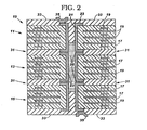
- assembly 10 is shown in FIG. 2.
- the preferred method of accomplishing such bonding is to use a conventional laminating process, which, in one example, is carried out at temperatures from about 70 to about 200 degrees Celsius (C.) for a time period of about 30 to about 180 minutes and under a laminating pressure of from about 50 to about 500 pounds per square inch (p.s.i.).
- a sticker sheet 31 is positioned between the respective substrates prior to lamination for the purpose of improving the bond between the substrates.
- the preferred sticker sheet material is defined hereinabove. It is understood, according to the broad aspects of the invention, that use of such a sticker sheet is not essential to achieve a satisfactory bond between the circuitized substrates taught herein.
- the bonded circuitized substrate assembly 10 is fully compressed as a result of the aforedefined lamination process.
- the conductive paste 25 has extended from its original position both upwardly and downwardly to partially fill the respective opposing openings 21 in substrates 11 and 15.
- paste 25 also extends between the opposing faces of the respective lands of layers 23 formed on the external surfaces of the respective substrates.
- an effective electrical connection has been attained between the conductive layers 23 of all three substrates using but a singular quantity of conductive paste 25.
- Such interim placement of conductive paste 25 between the lands further enhances the electrical connection between the respective substrates in the manner taught herein.
- Additional operations may now be performed on the bonded assembly 10, including the addition of another dielectric layer 33 and a conductive land 35 or the like which extends downwardly to contact the exposed land portion of a respective land portion of layer 23.
- Layer 33 may serve as a mounting layer or the like for additional electrical components (not shown) which may be positioned thereon.
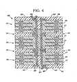
- FIG. 3 there is shown a bonded circuitized substrate assembly 10' according to an alternative embodiment of the invention.
- Assembly 10' includes the same components as shown in the embodiment of FIG. 1 with the exception that conductive paste is not filled within the opening 21 of substrate 13.
- a cover member 41 is provided over the external land portions of layer 23 of substrate 13.
- a preferred cover member is a metallic layer, e.g., copper.
- the opening in substrate 13 is preferably filled with a dielectric or other material (including conductive) 43.
- material 43 is a dielectric material of the type described above. With such dielectric material in place, cover members 41 may be plated over the external exposed surfaces of the positioned dielectric 43.
- cover layer 41 may include a thickness of from about 0.1 mils to about 2.0 mils.
- a quantity of conductive paste 25 is positioned over the cover member 41 and is comprised of a similar paste as used in the embodiment of FIG. 1.
- a quantity of 400 cubic mils of paste 25 is applied onto cover member 41 and will possess a thickness of only about 2 mils.
- two quantities of paste are utilized, but it is again understood that in the broadest aspects of this invention, only two substrates (11 and 13) may be utilized to form a successfully bonded final structure 10'.
- the exploded structure 10' in FIG. 3 is shown as being bonded, preferably using a lamination process as described above.
- the respective quantities of paste 25 have extended outwardly from the cover member 41 to partially fill the opening in the respective opposing substrate.
- a portion of the conductive paste 25 remains positioned between the external surfaces of the outwardly projecting land portions of the respective layers 23 to even further enhance the electrical coupling between the respective substrates.
- a dielectric 33' in addition to an external conductor 35', may also be added, including on opposite sides of the formed assembly 10'.
- circuitized substrate assembly comprised of at least two circuitized substrates, each including an opening therein which are aligned such that these openings can be electrically coupled during the subsequent bonding process.
- An assembly of the present invention provides significant wiring density increases over conventional printed circuit board constructions. This is primarily due to the fact that wiring PTHs no longer need to go through the entire assembly, but rather can stop on any given layer. Thus, wiring on the lower layers can be run unobstructed from any plated-thru-hole (PTH) blockages.
- PTH plated-thru-hole
- the present invention also eliminates the drill and plate concerns of high aspect ratio thru holes that are common with conventional circuit boards.
- the present invention provides a robust process and structure, while not requiring complete initial filling of all openings with paste prior to final joining, which would in turn require more exacting process tolerances to achieve high joining yield and reliable structures.
- such fillings would require the thickness of the 2 conductive pads to be joined plus the thickness of the conductive adhesive to be roughly equal to the sticker sheet. If the sticker sheet is thicker, then there could be poor contact of the conductive joints. If the pads plus paste are thicker than the sticker sheet, then there could be voids in the sticker sheet, or the conductive paste could be squeezed laterally, to the extent of possibly shorting adjacent pads.
- tolerance requirements were less than 1 mil, while the sum of the tolerance capabilities was significantly higher than 1 mil.
- the present invention substantially overcomes these problems.
Landscapes
- Engineering & Computer Science (AREA)
- Manufacturing & Machinery (AREA)
- Microelectronics & Electronic Packaging (AREA)
- Production Of Multi-Layered Print Wiring Board (AREA)
- Combinations Of Printed Boards (AREA)
- Insulated Metal Substrates For Printed Circuits (AREA)
Applications Claiming Priority (2)
| Application Number | Priority Date | Filing Date | Title |
|---|---|---|---|
| US10/322,527 US6809269B2 (en) | 2002-12-19 | 2002-12-19 | Circuitized substrate assembly and method of making same |
| US322527 | 2002-12-19 |
Publications (2)
| Publication Number | Publication Date |
|---|---|
| EP1432294A2 true EP1432294A2 (de) | 2004-06-23 |
| EP1432294A3 EP1432294A3 (de) | 2005-11-02 |
Family
ID=32393021
Family Applications (1)
| Application Number | Title | Priority Date | Filing Date |
|---|---|---|---|
| EP03257866A Withdrawn EP1432294A3 (de) | 2002-12-19 | 2003-12-15 | Leiterplattenanordnung und Verfahren zu deren Herstellung |
Country Status (6)
| Country | Link |
|---|---|
| US (6) | US6809269B2 (de) |
| EP (1) | EP1432294A3 (de) |
| JP (1) | JP2004200689A (de) |
| CN (1) | CN100579338C (de) |
| CA (1) | CA2452178C (de) |
| TW (1) | TWI288586B (de) |
Families Citing this family (43)
| Publication number | Priority date | Publication date | Assignee | Title |
|---|---|---|---|---|
| US6809269B2 (en) * | 2002-12-19 | 2004-10-26 | Endicott Interconnect Technologies, Inc. | Circuitized substrate assembly and method of making same |
| TW579665B (en) * | 2003-04-23 | 2004-03-11 | Via Tech Inc | Vertical routing structure |
| EP1649322A4 (de) | 2003-07-17 | 2007-09-19 | Honeywell Int Inc | Planarisierungsfilme für fortschrittliche mikroelektronsiche anwendungen und einrichtungen und herstellungsverfahren dafür |
| US20050041405A1 (en) * | 2003-08-22 | 2005-02-24 | Intel Corporation | Stacked via structure that includes a skip via |
| US7211289B2 (en) * | 2003-12-18 | 2007-05-01 | Endicott Interconnect Technologies, Inc. | Method of making multilayered printed circuit board with filled conductive holes |
| KR100584962B1 (ko) * | 2004-07-26 | 2006-05-29 | 삼성전기주식회사 | 액정 중합체로 커버레이 성형된 경연성 인쇄회로기판 및그 제조 방법 |
| US7698416B2 (en) * | 2005-01-25 | 2010-04-13 | Cisco Technology, Inc. | Application layer message-based server failover management by a network element |
| US20070013068A1 (en) * | 2005-06-17 | 2007-01-18 | Lsi Logic Corporation | Integrated circuit package and method with an electrical component embedded in a substrate via |
| US7342183B2 (en) * | 2005-07-11 | 2008-03-11 | Endicott Interconnect Technologies, Inc. | Circuitized substrate with sintered paste connections, multilayered substrate assembly, electrical assembly and information handling system utilizing same |
| US7334323B2 (en) * | 2005-07-11 | 2008-02-26 | Endicott Interconnect Technologies, Inc. | Method of making mutilayered circuitized substrate assembly having sintered paste connections |
| US7442879B2 (en) * | 2005-07-11 | 2008-10-28 | Endicott Interconect Technologies, Inc. | Circuitized substrate with solder-coated microparticle paste connections, multilayered substrate assembly, electrical assembly and information handling system utilizing same and method of making said substrate |
| US7211470B2 (en) * | 2005-09-01 | 2007-05-01 | Endicott Interconnect Technologies, Inc. | Method and apparatus for depositing conductive paste in circuitized substrate openings |
| US8063315B2 (en) | 2005-10-06 | 2011-11-22 | Endicott Interconnect Technologies, Inc. | Circuitized substrate with conductive paste, electrical assembly including said circuitized substrate and method of making said substrate |
| JP4821276B2 (ja) * | 2005-11-10 | 2011-11-24 | 住友電気工業株式会社 | 多層プリント配線板の製造方法及び多層プリント配線板 |
| US7629559B2 (en) * | 2005-12-19 | 2009-12-08 | Endicott Interconnect Technologies, Inc. | Method of improving electrical connections in circuitized substrates |
| US7514116B2 (en) * | 2005-12-30 | 2009-04-07 | Intel Corporation | Horizontal Carbon Nanotubes by Vertical Growth and Rolling |
| US7547577B2 (en) * | 2006-11-14 | 2009-06-16 | Endicott Interconnect Technologies, Inc. | Method of making circuitized substrate with solder paste connections |
| TWI389290B (zh) * | 2007-11-08 | 2013-03-11 | 財團法人工業技術研究院 | 晶片結構及其製程、晶片堆疊結構及其製程 |
| KR101046134B1 (ko) * | 2007-12-27 | 2011-07-01 | 삼성전기주식회사 | 세라믹 기판 및 그 제조방법과 이를 이용한 전기장치 |
| US20090178273A1 (en) * | 2008-01-15 | 2009-07-16 | Endicott Interconnect Technologies, Inc. | Method of making circuitized assembly including a plurality of circuitized substrates |
| US20090241332A1 (en) * | 2008-03-28 | 2009-10-01 | Lauffer John M | Circuitized substrate and method of making same |
| JP4482613B2 (ja) * | 2009-12-24 | 2010-06-16 | 新光電気工業株式会社 | 多層配線基板の製造方法 |
| US8304863B2 (en) * | 2010-02-09 | 2012-11-06 | International Business Machines Corporation | Electromigration immune through-substrate vias |
| US9351408B2 (en) * | 2010-04-22 | 2016-05-24 | I3 Electronics, Inc. | Coreless layer buildup structure with LGA and joining layer |
| US8680670B2 (en) | 2010-10-22 | 2014-03-25 | International Business Machines Corporation | Multi-chip module system with removable socketed modules |
| JP5533596B2 (ja) * | 2010-11-25 | 2014-06-25 | 富士通株式会社 | プリント配線板の製造方法、プリント配線板及び電子機器 |
| US8299371B2 (en) | 2010-12-20 | 2012-10-30 | Endicott Interconnect Technologies, Inc. | Circuitized substrate with dielectric interposer assembly and method |
| CN102548252A (zh) * | 2010-12-28 | 2012-07-04 | 富葵精密组件(深圳)有限公司 | 多层电路板及其制作方法 |
| KR101853815B1 (ko) * | 2011-05-30 | 2018-05-02 | 삼성전자주식회사 | 회로기판 조립체 및 회로기판의 조립 방법 |
| JP5002718B1 (ja) * | 2011-06-29 | 2012-08-15 | 株式会社東芝 | フレキシブルプリント配線板の製造方法、フレキシブルプリント配線板、及び電子機器 |
| KR101370119B1 (ko) | 2011-12-13 | 2014-03-04 | 엠파이어 테크놀로지 디벨롭먼트 엘엘씨 | 엘라스토머 접착 |
| FR2984073B1 (fr) * | 2011-12-13 | 2014-09-12 | Thales Sa | Procede de realisation de carte imprimee |
| US9668345B2 (en) * | 2012-03-30 | 2017-05-30 | Hitachi Chemical Company, Ltd. | Multilayer wiring board with metal foil wiring layer, wire wiring layer, and interlayer conduction hole |
| CN103517583B (zh) * | 2012-06-27 | 2016-09-28 | 富葵精密组件(深圳)有限公司 | 多层电路板及其制作方法 |
| JP2014192476A (ja) * | 2013-03-28 | 2014-10-06 | Fujitsu Ltd | プリント基板の半田実装方法及び半田実装構造 |
| CN106793524A (zh) * | 2017-02-10 | 2017-05-31 | 昆山元茂电子科技有限公司 | 印刷电路板的制造方法 |
| US20190335593A1 (en) * | 2018-04-26 | 2019-10-31 | Daeduck Electronics Co., Ltd. | Method of manufacturing the printed circuit board |
| WO2020131897A1 (en) * | 2018-12-17 | 2020-06-25 | Averatek Corporation | Three dimensional circuit formation |
| US10818586B1 (en) * | 2019-11-08 | 2020-10-27 | Advanced Semiconductor Engineering, Inc. | Substrate structure and method of manufacturing the same |
| KR102777648B1 (ko) * | 2020-01-16 | 2025-03-11 | 엘지이노텍 주식회사 | 인쇄회로기판 및 이의 제조 방법 |
| CN112739016B (zh) * | 2020-12-10 | 2023-03-14 | 惠州市特创电子科技股份有限公司 | 叠孔电路板及其制备方法 |
| JP2023183319A (ja) | 2022-06-15 | 2023-12-27 | 新光電気工業株式会社 | 積層基板及び積層基板の製造方法 |
| JP2023183320A (ja) | 2022-06-15 | 2023-12-27 | 新光電気工業株式会社 | 積層基板及び積層基板の製造方法 |
Family Cites Families (26)
| Publication number | Priority date | Publication date | Assignee | Title |
|---|---|---|---|---|
| JPS611088A (ja) * | 1984-06-14 | 1986-01-07 | 松下電器産業株式会社 | 導電回路の形成法 |
| JPS6130059A (ja) | 1984-07-20 | 1986-02-12 | Nec Corp | 半導体装置の製造方法 |
| US5229550A (en) * | 1990-10-30 | 1993-07-20 | International Business Machines Corporation | Encapsulated circuitized power core alignment and lamination |
| US5129142A (en) * | 1990-10-30 | 1992-07-14 | International Business Machines Corporation | Encapsulated circuitized power core alignment and lamination |
| US5367764A (en) * | 1991-12-31 | 1994-11-29 | Tessera, Inc. | Method of making a multi-layer circuit assembly |
| JP3057924B2 (ja) * | 1992-09-22 | 2000-07-04 | 松下電器産業株式会社 | 両面プリント基板およびその製造方法 |
| WO1996001497A1 (de) | 1994-07-05 | 1996-01-18 | Siemens Aktiengesellschaft | Verfahren zur herstellung einer dreidimensionalen schaltungsanordnung |
| JP3290041B2 (ja) | 1995-02-17 | 2002-06-10 | インターナショナル・ビジネス・マシーンズ・コーポレーション | 多層プリント基板、多層プリント基板の製造方法 |
| JP3116130B2 (ja) * | 1995-12-19 | 2000-12-11 | 住友金属工業株式会社 | Bga接続構造の形成方法 |
| US5796589A (en) * | 1995-12-20 | 1998-08-18 | Intel Corporation | Ball grid array integrated circuit package that has vias located within the solder pads of a package |
| DE19681758B4 (de) * | 1996-06-14 | 2006-09-14 | Ibiden Co., Ltd. | Einseitiges Schaltkreissubstrat für mehrlagige Schaltkreisplatine, mehrlagige Schaltkreisplatine und Verfahren zur Herstellung selbiger |
| JPH10270496A (ja) * | 1997-03-27 | 1998-10-09 | Hitachi Ltd | 電子装置、情報処理装置、半導体装置並びに半導体チップの実装方法 |
| JP2870530B1 (ja) * | 1997-10-30 | 1999-03-17 | 日本電気株式会社 | スタックモジュール用インターポーザとスタックモジュール |
| US6026564A (en) * | 1998-04-10 | 2000-02-22 | Ang Technologies Inc. | Method of making a high density multilayer wiring board |
| US6204456B1 (en) * | 1998-09-24 | 2001-03-20 | International Business Machines Corporation | Filling open through holes in a multilayer board |
| US6054761A (en) * | 1998-12-01 | 2000-04-25 | Fujitsu Limited | Multi-layer circuit substrates and electrical assemblies having conductive composition connectors |
| RU2133081C1 (ru) * | 1998-12-08 | 1999-07-10 | Таран Александр Иванович | Многослойная коммутационная плата (варианты) |
| US6452117B2 (en) * | 1999-08-26 | 2002-09-17 | International Business Machines Corporation | Method for filling high aspect ratio via holes in electronic substrates and the resulting holes |
| US6630630B1 (en) * | 1999-12-14 | 2003-10-07 | Matsushita Electric Industrial Co., Ltd. | Multilayer printed wiring board and its manufacturing method |
| US6388204B1 (en) | 2000-08-29 | 2002-05-14 | International Business Machines Corporation | Composite laminate circuit structure and methods of interconnecting the same |
| US6593534B2 (en) * | 2001-03-19 | 2003-07-15 | International Business Machines Corporation | Printed wiring board structure with z-axis interconnections |
| US6759600B2 (en) * | 2001-04-27 | 2004-07-06 | Shinko Electric Industries Co., Ltd. | Multilayer wiring board and method of fabrication thereof |
| US20020166697A1 (en) * | 2001-05-11 | 2002-11-14 | International Business Machines Corporation | Circuit board construction |
| US6459047B1 (en) | 2001-09-05 | 2002-10-01 | International Business Machines Corporation | Laminate circuit structure and method of fabricating |
| US6826830B2 (en) * | 2002-02-05 | 2004-12-07 | International Business Machines Corporation | Multi-layered interconnect structure using liquid crystalline polymer dielectric |
| US6809269B2 (en) * | 2002-12-19 | 2004-10-26 | Endicott Interconnect Technologies, Inc. | Circuitized substrate assembly and method of making same |
-
2002
- 2002-12-19 US US10/322,527 patent/US6809269B2/en not_active Expired - Lifetime
-
2003
- 2003-03-06 US US10/379,575 patent/US6872894B2/en not_active Expired - Lifetime
- 2003-12-05 CA CA002452178A patent/CA2452178C/en not_active Expired - Fee Related
- 2003-12-05 TW TW092134417A patent/TWI288586B/zh not_active IP Right Cessation
- 2003-12-15 JP JP2003416107A patent/JP2004200689A/ja active Pending
- 2003-12-15 EP EP03257866A patent/EP1432294A3/de not_active Withdrawn
- 2003-12-19 CN CN200310123253A patent/CN100579338C/zh not_active Expired - Fee Related
-
2004
- 2004-03-30 US US10/811,915 patent/US7047630B2/en not_active Expired - Fee Related
- 2004-08-11 US US10/915,483 patent/US7071423B2/en not_active Expired - Lifetime
- 2004-09-03 US US10/933,260 patent/US6900392B2/en not_active Expired - Lifetime
-
2006
- 2006-02-09 US US11/349,998 patent/US7343674B2/en not_active Expired - Lifetime
Also Published As
| Publication number | Publication date |
|---|---|
| US20040177998A1 (en) | 2004-09-16 |
| US20060123626A1 (en) | 2006-06-15 |
| EP1432294A3 (de) | 2005-11-02 |
| US20050023035A1 (en) | 2005-02-03 |
| US7047630B2 (en) | 2006-05-23 |
| US6872894B2 (en) | 2005-03-29 |
| US20050011670A1 (en) | 2005-01-20 |
| CA2452178A1 (en) | 2004-06-19 |
| US7071423B2 (en) | 2006-07-04 |
| CN100579338C (zh) | 2010-01-06 |
| TW200507705A (en) | 2005-02-16 |
| US6900392B2 (en) | 2005-05-31 |
| CN1553763A (zh) | 2004-12-08 |
| CA2452178C (en) | 2008-05-13 |
| US20040118596A1 (en) | 2004-06-24 |
| US7343674B2 (en) | 2008-03-18 |
| JP2004200689A (ja) | 2004-07-15 |
| US20040118598A1 (en) | 2004-06-24 |
| US6809269B2 (en) | 2004-10-26 |
| TWI288586B (en) | 2007-10-11 |
Similar Documents
| Publication | Publication Date | Title |
|---|---|---|
| CA2452178C (en) | Circuitized substrate assembly and method of making same | |
| US6479093B2 (en) | Composite laminate circuit structure and methods of interconnecting the same | |
| US5229550A (en) | Encapsulated circuitized power core alignment and lamination | |
| US5129142A (en) | Encapsulated circuitized power core alignment and lamination | |
| US6645607B2 (en) | Method and structure for producing Z-axis interconnection assembly of printed wiring board elements | |
| TWI430728B (zh) | 製造具有焊料膏連接之電路化基板的方法 | |
| US7076869B2 (en) | Solid via layer to layer interconnect | |
| US20090241332A1 (en) | Circuitized substrate and method of making same | |
| US6638607B1 (en) | Method and structure for producing Z-axis interconnection assembly of printed wiring board elements | |
| US8541687B2 (en) | Coreless layer buildup structure | |
| KR20010075727A (ko) | 국부적으로 향상된 배선밀도를 가진 인쇄회로어셈블리 | |
| US6905589B2 (en) | Circuitized substrate and method of making same | |
| US20120031649A1 (en) | Coreless layer buildup structure with lga and joining layer | |
| JPH08330736A (ja) | 多層基板およびその製造方法 | |
| US8536459B2 (en) | Coreless layer buildup structure with LGA | |
| JPH1131882A (ja) | 多層配線板およびその製造方法 | |
| JPH11135943A (ja) | 多層プリント配線板の製造方法 | |
| JPH1126052A (ja) | 厚さ方向導電シート及びその製造方法 |
Legal Events
| Date | Code | Title | Description |
|---|---|---|---|
| PUAI | Public reference made under article 153(3) epc to a published international application that has entered the european phase |
Free format text: ORIGINAL CODE: 0009012 |
|
| AK | Designated contracting states |
Kind code of ref document: A2 Designated state(s): AT BE BG CH CY CZ DE DK EE ES FI FR GB GR HU IE IT LI LU MC NL PT RO SE SI SK TR |
|
| AX | Request for extension of the european patent |
Extension state: AL LT LV MK |
|
| PUAL | Search report despatched |
Free format text: ORIGINAL CODE: 0009013 |
|
| AK | Designated contracting states |
Kind code of ref document: A3 Designated state(s): AT BE BG CH CY CZ DE DK EE ES FI FR GB GR HU IE IT LI LU MC NL PT RO SE SI SK TR |
|
| AX | Request for extension of the european patent |
Extension state: AL LT LV MK |
|
| 17P | Request for examination filed |
Effective date: 20060419 |
|
| AKX | Designation fees paid |
Designated state(s): BE DE FR GB IT NL |
|
| STAA | Information on the status of an ep patent application or granted ep patent |
Free format text: STATUS: THE APPLICATION IS DEEMED TO BE WITHDRAWN |
|
| 18D | Application deemed to be withdrawn |
Effective date: 20110701 |