EP1432585B1 - Tintenstrahldruckkopfanordnung auf klebstoffbasis - Google Patents
Tintenstrahldruckkopfanordnung auf klebstoffbasis Download PDFInfo
- Publication number
- EP1432585B1 EP1432585B1 EP02750664A EP02750664A EP1432585B1 EP 1432585 B1 EP1432585 B1 EP 1432585B1 EP 02750664 A EP02750664 A EP 02750664A EP 02750664 A EP02750664 A EP 02750664A EP 1432585 B1 EP1432585 B1 EP 1432585B1
- Authority
- EP
- European Patent Office
- Prior art keywords
- print head
- ink jet
- jet print
- head chip
- chip
- Prior art date
- Legal status (The legal status is an assumption and is not a legal conclusion. Google has not performed a legal analysis and makes no representation as to the accuracy of the status listed.)
- Expired - Lifetime
Links
Images



Classifications
-
- B—PERFORMING OPERATIONS; TRANSPORTING
- B41—PRINTING; LINING MACHINES; TYPEWRITERS; STAMPS
- B41J—TYPEWRITERS; SELECTIVE PRINTING MECHANISMS, i.e. MECHANISMS PRINTING OTHERWISE THAN FROM A FORME; CORRECTION OF TYPOGRAPHICAL ERRORS
- B41J2/00—Typewriters or selective printing mechanisms characterised by the printing or marking process for which they are designed
- B41J2/005—Typewriters or selective printing mechanisms characterised by the printing or marking process for which they are designed characterised by bringing liquid or particles selectively into contact with a printing material
- B41J2/01—Ink jet
- B41J2/135—Nozzles
- B41J2/16—Production of nozzles
-
- B—PERFORMING OPERATIONS; TRANSPORTING
- B41—PRINTING; LINING MACHINES; TYPEWRITERS; STAMPS
- B41J—TYPEWRITERS; SELECTIVE PRINTING MECHANISMS, i.e. MECHANISMS PRINTING OTHERWISE THAN FROM A FORME; CORRECTION OF TYPOGRAPHICAL ERRORS
- B41J2/00—Typewriters or selective printing mechanisms characterised by the printing or marking process for which they are designed
- B41J2/005—Typewriters or selective printing mechanisms characterised by the printing or marking process for which they are designed characterised by bringing liquid or particles selectively into contact with a printing material
- B41J2/01—Ink jet
- B41J2/17—Ink jet characterised by ink handling
- B41J2/175—Ink supply systems ; Circuit parts therefor
-
- B—PERFORMING OPERATIONS; TRANSPORTING
- B41—PRINTING; LINING MACHINES; TYPEWRITERS; STAMPS
- B41J—TYPEWRITERS; SELECTIVE PRINTING MECHANISMS, i.e. MECHANISMS PRINTING OTHERWISE THAN FROM A FORME; CORRECTION OF TYPOGRAPHICAL ERRORS
- B41J2/00—Typewriters or selective printing mechanisms characterised by the printing or marking process for which they are designed
- B41J2/005—Typewriters or selective printing mechanisms characterised by the printing or marking process for which they are designed characterised by bringing liquid or particles selectively into contact with a printing material
- B41J2/01—Ink jet
- B41J2/135—Nozzles
- B41J2/14—Structure thereof only for on-demand ink jet heads
-
- B—PERFORMING OPERATIONS; TRANSPORTING
- B41—PRINTING; LINING MACHINES; TYPEWRITERS; STAMPS
- B41J—TYPEWRITERS; SELECTIVE PRINTING MECHANISMS, i.e. MECHANISMS PRINTING OTHERWISE THAN FROM A FORME; CORRECTION OF TYPOGRAPHICAL ERRORS
- B41J2/00—Typewriters or selective printing mechanisms characterised by the printing or marking process for which they are designed
- B41J2/005—Typewriters or selective printing mechanisms characterised by the printing or marking process for which they are designed characterised by bringing liquid or particles selectively into contact with a printing material
- B41J2/01—Ink jet
- B41J2/135—Nozzles
- B41J2/145—Arrangement thereof
- B41J2/155—Arrangement thereof for line printing
-
- B—PERFORMING OPERATIONS; TRANSPORTING
- B41—PRINTING; LINING MACHINES; TYPEWRITERS; STAMPS
- B41J—TYPEWRITERS; SELECTIVE PRINTING MECHANISMS, i.e. MECHANISMS PRINTING OTHERWISE THAN FROM A FORME; CORRECTION OF TYPOGRAPHICAL ERRORS
- B41J2/00—Typewriters or selective printing mechanisms characterised by the printing or marking process for which they are designed
- B41J2/005—Typewriters or selective printing mechanisms characterised by the printing or marking process for which they are designed characterised by bringing liquid or particles selectively into contact with a printing material
- B41J2/01—Ink jet
- B41J2/135—Nozzles
- B41J2/16—Production of nozzles
- B41J2/1621—Manufacturing processes
- B41J2/1623—Manufacturing processes bonding and adhesion
-
- B—PERFORMING OPERATIONS; TRANSPORTING
- B41—PRINTING; LINING MACHINES; TYPEWRITERS; STAMPS
- B41J—TYPEWRITERS; SELECTIVE PRINTING MECHANISMS, i.e. MECHANISMS PRINTING OTHERWISE THAN FROM A FORME; CORRECTION OF TYPOGRAPHICAL ERRORS
- B41J2/00—Typewriters or selective printing mechanisms characterised by the printing or marking process for which they are designed
- B41J2/005—Typewriters or selective printing mechanisms characterised by the printing or marking process for which they are designed characterised by bringing liquid or particles selectively into contact with a printing material
- B41J2/01—Ink jet
- B41J2/135—Nozzles
- B41J2/165—Prevention or detection of nozzle clogging, e.g. cleaning, capping or moistening for nozzles
- B41J2/16517—Cleaning of print head nozzles
- B41J2/16535—Cleaning of print head nozzles using wiping constructions
- B41J2/16538—Cleaning of print head nozzles using wiping constructions with brushes or wiper blades perpendicular to the nozzle plate
-
- B—PERFORMING OPERATIONS; TRANSPORTING
- B41—PRINTING; LINING MACHINES; TYPEWRITERS; STAMPS
- B41J—TYPEWRITERS; SELECTIVE PRINTING MECHANISMS, i.e. MECHANISMS PRINTING OTHERWISE THAN FROM A FORME; CORRECTION OF TYPOGRAPHICAL ERRORS
- B41J2/00—Typewriters or selective printing mechanisms characterised by the printing or marking process for which they are designed
- B41J2/005—Typewriters or selective printing mechanisms characterised by the printing or marking process for which they are designed characterised by bringing liquid or particles selectively into contact with a printing material
- B41J2/01—Ink jet
- B41J2/135—Nozzles
- B41J2/14—Structure thereof only for on-demand ink jet heads
- B41J2002/14362—Assembling elements of heads
-
- B—PERFORMING OPERATIONS; TRANSPORTING
- B41—PRINTING; LINING MACHINES; TYPEWRITERS; STAMPS
- B41J—TYPEWRITERS; SELECTIVE PRINTING MECHANISMS, i.e. MECHANISMS PRINTING OTHERWISE THAN FROM A FORME; CORRECTION OF TYPOGRAPHICAL ERRORS
- B41J2202/00—Embodiments of or processes related to ink-jet or thermal heads
- B41J2202/01—Embodiments of or processes related to ink-jet heads
- B41J2202/19—Assembling head units
-
- B—PERFORMING OPERATIONS; TRANSPORTING
- B41—PRINTING; LINING MACHINES; TYPEWRITERS; STAMPS
- B41J—TYPEWRITERS; SELECTIVE PRINTING MECHANISMS, i.e. MECHANISMS PRINTING OTHERWISE THAN FROM A FORME; CORRECTION OF TYPOGRAPHICAL ERRORS
- B41J2202/00—Embodiments of or processes related to ink-jet or thermal heads
- B41J2202/01—Embodiments of or processes related to ink-jet heads
- B41J2202/20—Modules
Definitions
- This invention relates to a print head assembly. More particularly, this invention relates to a print head assembly and to a method of assembling a print head.
- the Applicant has developed a page width ink jet print head that is the subject of a large number of United States patents and patent applications.
- the print head is capable of printing text and images having resolutions as high as 1600dpi.
- print head chips are the product of an integrated circuit fabrication technique.
- each print head chip comprises a plurality of nozzle arrangements that are positioned along a length of silicon wafer substrate.
- Each nozzle arrangement is in the form of a micro electro-mechanical system. The applicant has developed technology that allows for the fabrication of such print heads having up to 84 000 nozzle arrangements.
- EP-A-082208 discloses an inkjet printhead assembly comprising a printhead chip bonded to a support member. The chip is positioned in a chip installation hole, defined by an electrical wiring substrate.
- DE 196 12 760 discloses a carrier plate providing an electric connector structure for connecting electronic components.
- the print head chips are positioned in some form of carrier.
- the carrier forms part of an ink distribution arrangement such as an ink distribution manifold.
- the carrier can itself be attached in some way to an ink distribution arrangement to define some form of interface between the print bead chips and the ink distribution arrangement.
- the positioning of the print head chips in their respective carriers usually takes place by way of simply urging the print head chip into a recess defined in the carrier,
- the recess is thus dimensioned so that the fit is a snug fit or an interference fit to ensure that the print head chip is retained in position in the carrier.
- the print head chip Due to the elongate nature of the print head chip, the print head chip is susceptible to flexure. As a result, any stresses that are exerted on the carrier during normal handling and operation can result in flexure of the carrier and thus the print head chip. It will be appreciated by those of ordinary skill in the art that the fact that the nozzle arrangements are each in the form of a micro electro-mechanical system makes such flexure highly undesirable.
- a particular problem with such a fit stems from the possible ingress of particulate matter into the recess. This is especially so if the matter is in the form of one or more relatively hard particles.
- the chip When the chip is urged into the recess, such a particle can become sandwiched between the print head chip and a wall of the recess. This results in a region of stress concentration at that point on the print head chip that is impinged upon by the particle.
- the stress concentration can cause a fracturing of the print head chip.
- the Applicant has conceived the present invention to address this problem and to alleviate the necessity for the print head manufacturer to achieve a particulate free environment for the assembly stage of the print head.
- chip manufacturers incur substantial expense to ensure that chip fabrication environments are kept sterile. Applicant believes that it is desirable that the need for such sterile environments does not extend to the print head assembly stage.
- an ink jet print head assembly that comprises
- an ink jet print head having at least one elongate ink jet print head chip that is the product of an integrated circuit fabrication technique and at least one corresponding ink jet print head chip carrier that defines an elongate recess having a pair of opposed side walls, the, or each, ink jet print head chip and said respective recess being dimensioned so that a width of said the, or each, print head chip is less than a width of said respective recess to a predetermined extent, the method comprising the steps of
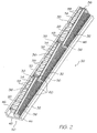
- reference numeral 10 generally indicates a first embodiment of an ink jet print head assembly, in accordance with the invention.
- the ink jet print head assembly 10 is in the form of a page width ink jet print head.
- the ink jet print head assembly 10 includes an ink jet print head chip carrier 14.
- An ink distribution manifold 12 is positioned on the carrier 14.
- the ink jet print head chip carrier 14 includes a support member 16.
- An elongate recess or channel 18 is defined in the support member 16.
- the ink jet print head 10 includes a number of ink jet print head chips, one of which is indicated at 20.
- the ink jet print head chip 20 is the product of an integrated circuit fabrication technique. Further, the ink jet print head chip 20 comprises a plurality of nozzle arrangements (not shown). Each nozzle arrangement is in the form of a micro electro-mechanical system. Thus, each nozzle arrangement has at least one moving component that acts on ink within a nozzle chamber to eject that ink from the nozzle chamber.
- the ink jet print head chip 20 and the channel 18 both have a rectangular cross section, with the channel 18 being larger than the ink jet print head chip 20, to a predetermined extent.
- a width of the channel 18 is larger, to a predetermined extent, than the print head chip 20.
- a width of the channel 18 can be between approximately 310 microns and 5100 microns.
- a width of the ink jet print head chip 20 can be between approximately 300 microns and 5000 microns.
- the chip 20 is inserted into the channel 18 as shown by the arrow 21.
- the ink jet print head chip 20 is fixed in the channel 18 with an adhesive that, when cured, defines a resiliently flexible material, indicated at 22.
- a gap 26 is set up between each side 24 of the print head chip 20 and a corresponding side wall 28 defining the channel 18.
- the gap 26 therefore has a width of between approximately 5 and 50 microns.
- the gaps 26 are filled with the resiliently flexible material 22.
- the print head chip 20 has an extremely high length to width ratio.
- the reason for this is that the fabrication process allows the Applicant to conserve chip real estate by keeping the width of the chip 20 as small as possible, while retaining a substantial length to permit page width printing.
- the carrier 14 and the ink distribution manifold 12 also have relatively high length to width ratios. It follows that the print head 10 is susceptible to flexure during normal handling and operation. It will be appreciated that, without the gap 26, this flexure would be transmitted directly to the print head chip 20, which would be undesirable.
- the gaps 26 allow for a certain amount of flexure of the carrier 14 without this flexure being transmitted to the chip 20.
- the adhesive once cured into the resiliently flexible material 22, serves to accommodate flexure of the carrier 14, while retaining the chip 20 in position in the channel 18.
- the adhesive is of the type that cures into an elastomeric material.
- the adhesive is a silicon rubber adhesive.
- reference numeral 30 generally indicates a second embodiment of an ink jet print head assembly, in accordance with the invention.
- like reference numerals refer to like parts, unless otherwise specified.
- the print head assembly 30 is similar to the print head assembly that is the subject of the above referenced US patent application no's 09/693,644, 09/693,737 and 09/696,340. It follows that this description will be limited to the manner in which the print head chip 20 is mounted and will not set out further detail that is already set out in the above US patent applications, except in a broad fashion.
- the print head assembly 30 is a modular print head assembly having a number of modules 32.
- Each module 32 has a carrier 34 that defines a channel 36 in which the print head chip 20 is received.
- the relative dimensions of the channel 36 and the print head chip 20 are the same as those of the print head assembly 10. It follows that a gap 38 is also defined between each side 24 of the print head chip 20 and a corresponding side wall 40 of the channel 36.
- the print head chip 10 is fixed in its respective channel 36 with an adhesive that cures into a resiliently flexible material, indicated at 42.
- the benefits of the gaps 38 and the resiliently flexible material 42 are set out above.
- the print head 30 includes a retaining structure 44 in which the modules 32 are positioned.
- Each carrier 34 is in the form of a tile that is mounted in the retaining structure 44.
- the retaining structure 44 has a pair of opposed side portions 46 and a floor portion 48, which define a region 50 in which the tiles 34 are mounted.
- the tiles 34 each define nesting formations 56 so that the tiles 34 can nest together in an end-to-end manner along the region 50. Details of the manner in which the tiles 34 are positioned in the region 50 are set out in the above referenced patent applications.
- Each tile 34 has a first molding 52 that is positioned on a second molding 54, with both moldings 52, 54 mounted in the region 50 of the retaining structure 44. Structural details of the moldings 52, 54 are provided in the above referenced patent applications.
- the channel 36 is defined in the first molding 52.
- a plurality of raised ribs 58 is defined by the first molding 52 on one side of the channel 36.
- the raised ribs 58 serve to maintain print media passing over the print head chip 20 at a desired spacing from the print head chip 20.
- a plurality of conductive strips 60 is defined on an opposed side of the channel 36. The strips 60 are wired to electrical contacts of the chip 20 to connect control circuitry (not shown) to the print head chip 20.
- the first molding 52 defines a recess 62 approximately midway along its length.
- the recess 62 is positioned and dimensioned to engage a catch 64 defined by one of the side portions 46 of the retaining structure 44, when the tile 34 is mounted in the region 50 of the retaining structure 44. Again, details of the manner in which the tiles 34 are mounted in the retaining structure 44 are provided in the above referenced applications.
- the first molding 52 has a plurality of inlet openings 66 defined therein.
- the openings 66 are used to supply ink to the print head chip 20.
- openings 66 are in fluid communication with corresponding openings 68 defined at longitudinally spaced intervals in the second molding 54.
- openings 70 are defined in the molding 54 for the supply of air. Further details are provided in the above referenced applications.
- the tiles 34 and the retaining structure 44 are configured so that a certain amount of relative movement between the tiles 34 and the retaining structure 44 can be accommodated. Details of how this is achieved are set out in the above referenced applications.
- collared structures 72 are positioned on the floor portion 48 of the retaining structure 44.
- the collared structures 72 are of a resiliently flexible hydrophobic material and engage complementary recesses defined in the second molding 54. Thus, a tight seal is maintained, in spite of such relative movement.
- the collars 72 circumscribe openings of passages 74 ( Figure 8) defined in the floor portion 48. Again, further details are provided in the above referenced applications.
- the passages 74 are in fluid communication with the openings 68 in the second mounting, which, in turn, are in fluid communication with the openings 66.
- the passages 74 are divided into six sets that can receive, for example, cyan, yellow, magenta, black and infrared inks and fixative respectively. Other combinations of up to six types of ink can be used. It follows that the chip 20 is a "six color" chip.
- the print head 30 includes a nozzle guard 76 that covers a nozzle layer 78.
- the nozzle layer 78 is mounted on a silicon inlet backing 80 as described in greater detail in the above referenced US patent application number 09/608, 779.
- gaps 38 together with the resiliently flexible material 42 provides a means whereby a point of stress concentration that may result from the ingress of particulate matter between the chip 20 and the sidewalls 40 of the channels 36 can be avoided.
- the gaps 38 and the resiliently flexible material 42 obviate the need for press fitting or even snugly fitting the chips 20 in their respective channels 36.
- the detrimental effects of the ingress of such particulate matter are alleviated to a substantial extent.
Landscapes
- Engineering & Computer Science (AREA)
- Manufacturing & Machinery (AREA)
- Particle Formation And Scattering Control In Inkjet Printers (AREA)
- Adhesives Or Adhesive Processes (AREA)
Claims (7)
- - Tintenstrahldruckkopfanordnung (10) für einen seitenbreiten Tintenstrahldruckkopf, wobei die Druckkopfanordnung
mindestens einen länglichen Tintenstrahldruckkopfchip (20), der das Produkt einer integrierten Schaltkreisfertigungstechnik ist ;
mindestens einen entsprechenden Tintenstrahldruckkopfchipträger (14), der eine längliche Aussparung (18) mit einem Paar gegenüberliegender Seitenwände (28) definiert, wobei der oder jeder Druckkopfchip (20) in einer jeweiligen Aussparung aufgenommen wird, wobei der oder jeder Tintenstrahldruckkopfchip und die jeweilige Aussparung so dimensioniert sind, dass ein Spalt (26) zwischen dem oder jedem Tintenstrahldruckkopfchip (20) und jeder Seitenwand (28) definiert wird, umfasst ; und
gekennzeichnet durch :federnd verformbares Material (22), das in jedem Spalt (26) positioniert ist, um jeden Spalt zu füllen und den oder jeden Druckkopfchip in der jeweiligen Aussparung (18) in Position zu halten, wobei das federnd verformbare Material (22) so ausgewählt ist, dass es sich an eine relative Bewegung des wenigstens einen Druckkopfchips (20) und des wenigstens einen Druckkopfchipträgers (14) während normaler Handhabung der Druckkopfanordnung (10) anpasst. - - Tintenstrahldruckkopfanordnung, wie in Anspruch 1 beansprucht, welche eine Anzahl der Tintenstrahldruckkopfchips (20) umfasst, die in den länglichen Aussparungen (18) der Tintenstrahldruckkopfchipträger (14), die den Tintenstrahldruckkopfchips entsprechen, positioniert sind.
- - Tintenstrahldruckkopfanordnung, wie in Anspruch 1 beansprucht, wobei der Tintenstrahldruckkopfchipsträger (14) an einen Verteiler zur Tintenverteilung montiert ist.
- - Tintenstrahldruckkopfanordnung, wie in Anspruch 1 beansprucht, welche eine Anzahl von Modulen (32) umfasst, wobei jedes Modul einen Tintenstrahldruckkopfchipträger (14) und einen in dem Träger montierten Tintenstrahldruckkopfchip (20) und eine Rückhaltestruktur (44), worin die Module montiert sind, umfasst.
- - Tintenstrahldruckkopfanordnung, wie in Anspruch 1 beansprucht, wobei das federnd verformbare Material (22) ein Elastomermaterial ist.
- - Tintenstrahldruckkopfanordnung, wie in Anspruch 5 beansprucht, worin das Elastomermaterial in Form eines Materials auf Siliziumbasis vorliegt.
- - Verfahren zum Zusammenbau eines Tintenstrahldruckkopfs mit mindestens einem länglichen Tintenstrahldruckkopfchip (20), der das Produkt einer integrierten Schaltkreisfertigungstechnik ist, und mindestens einem entsprechenden Tintenstrahldruckkopfchipträger (14), der eine längliche Aussparung (18) mit einem Paar gegenüberliegender Seitenwände (28) definiert, wobei der oder jeder Tintenstrahldruckkopfchip (20) und die jeweilige Aussparung so dimensioniert sind, dass eine Breite des oder jedes Druckkopfchips kleiner ist als eine Breite der jeweiligen Aussparung in einem vorbestimmten Ausmaß ist,
wobei das Verfahren die Schritte umfasst des :Positionierens des oder jedes Tintenstrahldruckkopfchips (20) in dem jeweiligen Träger, sodass ein Spalt (26) an jeder der beiden Seiten des Tintenstrahldruckkopfchips durch das Paar gegenüberliegender Seitenwände (28) und den Tintenstrahldruckkopfchip (20) definiert wird ; undgekennzeichnet durchFüllen jeden Spalts (26) mit einem Klebstoff (22), der aus einer Gruppe von Klebstoffen gewählt ist, die zu einem federnd verformbaren Material aushärten, um den oder jeden Tintenstrahldruckkopfchip (20) in der jeweiligen Aussparung (18) zu fixieren, wobei der Klebstoff so gewählt ist, dass das federnd verformbare Material fähig ist, sich an die relative Bewegung des oder jedes Druckkopfchips (20) und des oder jedes Druckkopfchipträgers (14) während normaler Handhabung anzupassen.
Applications Claiming Priority (3)
| Application Number | Priority Date | Filing Date | Title |
|---|---|---|---|
| US942549 | 2001-08-31 | ||
| US09/942,549 US6616271B2 (en) | 1999-10-19 | 2001-08-31 | Adhesive-based ink jet print head assembly |
| PCT/AU2002/001057 WO2003018317A1 (en) | 2001-08-31 | 2002-08-06 | An adhesive-based ink jet print head assembly |
Publications (3)
| Publication Number | Publication Date |
|---|---|
| EP1432585A1 EP1432585A1 (de) | 2004-06-30 |
| EP1432585A4 EP1432585A4 (de) | 2005-12-21 |
| EP1432585B1 true EP1432585B1 (de) | 2007-04-11 |
Family
ID=25478254
Family Applications (1)
| Application Number | Title | Priority Date | Filing Date |
|---|---|---|---|
| EP02750664A Expired - Lifetime EP1432585B1 (de) | 2001-08-31 | 2002-08-06 | Tintenstrahldruckkopfanordnung auf klebstoffbasis |
Country Status (11)
| Country | Link |
|---|---|
| US (4) | US6616271B2 (de) |
| EP (1) | EP1432585B1 (de) |
| JP (1) | JP2005500192A (de) |
| KR (1) | KR100601837B1 (de) |
| CN (1) | CN1274505C (de) |
| AT (1) | ATE359181T1 (de) |
| AU (1) | AU2002356075B2 (de) |
| CA (1) | CA2458599C (de) |
| DE (1) | DE60219494D1 (de) |
| IL (1) | IL160625A (de) |
| WO (1) | WO2003018317A1 (de) |
Families Citing this family (22)
| Publication number | Priority date | Publication date | Assignee | Title |
|---|---|---|---|---|
| AUPQ439299A0 (en) | 1999-12-01 | 1999-12-23 | Silverbrook Research Pty Ltd | Interface system |
| ATE292562T1 (de) * | 1999-06-30 | 2005-04-15 | Silverbrook Res Pty Ltd | Trägerstruktur und trägeranordnung für einen druckkopf |
| US20050212830A1 (en) * | 1999-09-17 | 2005-09-29 | Silverbrook Research Pty Ltd | Method of accessing a connection address using a mobile device with a sensing means |
| US6616271B2 (en) * | 1999-10-19 | 2003-09-09 | Silverbrook Research Pty Ltd | Adhesive-based ink jet print head assembly |
| US7677698B2 (en) * | 1999-12-09 | 2010-03-16 | Silverbrook Research Pty Ltd | Modular printhead assembly with reservoir mounted printhead modules |
| US6786658B2 (en) * | 2000-05-23 | 2004-09-07 | Silverbrook Research Pty. Ltd. | Printer for accommodating varying page thicknesses |
| DE60023952T2 (de) * | 2000-05-24 | 2006-12-07 | Silverbrook Research Pty. Ltd. | Sensor für die papierdicke in einem printer |
| US6755509B2 (en) * | 2002-11-23 | 2004-06-29 | Silverbrook Research Pty Ltd | Thermal ink jet printhead with suspended beam heater |
| KR100612322B1 (ko) * | 2004-07-16 | 2006-08-16 | 삼성전자주식회사 | 잉크젯 카트리지 |
| GB0416523D0 (en) | 2004-07-23 | 2004-08-25 | Xaar Technology Ltd | Method of manufacture |
| US20060250477A1 (en) * | 2005-05-09 | 2006-11-09 | Silverbrook Research Pty Ltd | Cartridge with capping mechanism for use in a mobile device |
| US7753517B2 (en) * | 2005-05-09 | 2010-07-13 | Silverbrook Research Pty Ltd | Printhead with an optical sensor for receiving print data |
| US7284921B2 (en) * | 2005-05-09 | 2007-10-23 | Silverbrook Research Pty Ltd | Mobile device with first and second optical pathways |
| US8657413B2 (en) * | 2011-01-18 | 2014-02-25 | Funai Electric Co., Ltd. | Die attach composition for silicon chip placement on a flat substrate having improved thixotropic properties |
| US8636340B2 (en) * | 2011-03-14 | 2014-01-28 | Funai Electric Co., Ltd. | Printheads and method for assembling printheads |
| US9440441B2 (en) | 2012-12-03 | 2016-09-13 | Hewlett-Packard Development Company, L.P. | Multi-part fluid flow structure |
| KR101827070B1 (ko) | 2013-02-28 | 2018-02-07 | 휴렛-팩커드 디벨롭먼트 컴퍼니, 엘.피. | 유체 유동 구조체 성형 |
| US10821729B2 (en) | 2013-02-28 | 2020-11-03 | Hewlett-Packard Development Company, L.P. | Transfer molded fluid flow structure |
| EP3296113B1 (de) | 2013-02-28 | 2019-08-28 | Hewlett-Packard Development Company, L.P. | Geformter druckbalken |
| US9724920B2 (en) | 2013-03-20 | 2017-08-08 | Hewlett-Packard Development Company, L.P. | Molded die slivers with exposed front and back surfaces |
| US9996857B2 (en) | 2015-03-17 | 2018-06-12 | Dow Jones & Company, Inc. | Systems and methods for variable data publication |
| JP2018134835A (ja) * | 2017-02-23 | 2018-08-30 | セイコーエプソン株式会社 | 液体噴射ヘッド、液体噴射装置、及び、液体噴射ヘッドの製造方法 |
Family Cites Families (21)
| Publication number | Priority date | Publication date | Assignee | Title |
|---|---|---|---|---|
| US3556A (en) * | 1844-04-20 | Churn | ||
| US4554558A (en) | 1983-05-19 | 1985-11-19 | The Mead Corporation | Fluid jet print head |
| US5181932A (en) * | 1989-04-13 | 1993-01-26 | Phillips L Van | Foot prosthesis having auxiliary ankle construction |
| US4812859A (en) | 1987-09-17 | 1989-03-14 | Hewlett-Packard Company | Multi-chamber ink jet recording head for color use |
| AU657720B2 (en) * | 1991-01-30 | 1995-03-23 | Canon Kabushiki Kaisha | A bubblejet image reproducing apparatus |
| US5565900A (en) * | 1994-02-04 | 1996-10-15 | Hewlett-Packard Company | Unit print head assembly for ink-jet printing |
| US5665249A (en) | 1994-10-17 | 1997-09-09 | Xerox Corporation | Micro-electromechanical die module with planarized thick film layer |
| DE19612760C2 (de) | 1996-03-29 | 2002-01-10 | Oce Printing Systems Gmbh | Trägerplatte und Druckkopf mit dieser Trägerplatte |
| US6257703B1 (en) * | 1996-07-31 | 2001-07-10 | Canon Kabushiki Kaisha | Ink jet recording head |
| US6084612A (en) | 1996-07-31 | 2000-07-04 | Canon Kabushiki Kaisha | Liquid ejection head, liquid ejection head cartridge, printing apparatus, printing system and fabrication process of liquid ejection head |
| US6168265B1 (en) | 1997-03-28 | 2001-01-02 | Brother Kogyo Kabushiki Kaisha | Ink-jet print head |
| AUPP653698A0 (en) * | 1998-10-16 | 1998-11-05 | Silverbrook Research Pty Ltd | Micromechanical fluid supply system (fluid08) |
| US6318849B1 (en) * | 1997-07-15 | 2001-11-20 | Silverbrook Research Pty Ltd | Fluid supply mechanism for multiple fluids to multiple spaced orifices |
| US6616271B2 (en) * | 1999-10-19 | 2003-09-09 | Silverbrook Research Pty Ltd | Adhesive-based ink jet print head assembly |
| US6190002B1 (en) * | 1999-10-27 | 2001-02-20 | Lexmark International, Inc. | Ink jet pen |
| JP2001150680A (ja) | 1999-11-29 | 2001-06-05 | Casio Comput Co Ltd | インクジェットプリンタヘッド |
| JP3592208B2 (ja) * | 2000-07-10 | 2004-11-24 | キヤノン株式会社 | 液体噴射記録ヘッドおよびその製造方法 |
| US6457810B1 (en) * | 2000-10-20 | 2002-10-01 | Silverbrook Research Pty Ltd. | Method of assembly of six color inkjet modular printhead |
| US6485135B1 (en) * | 2000-10-20 | 2002-11-26 | Silverbrook Research Pty Ltd | Ink feed for six color inkjet modular printhead |
| US6575559B2 (en) * | 2001-10-31 | 2003-06-10 | Hewlett-Packard Development Company, L.P. | Joining of different materials of carrier for fluid ejection devices |
| TWI259149B (en) * | 2002-09-30 | 2006-08-01 | Canon Kk | Ink container and recording apparatus |
-
2001
- 2001-08-31 US US09/942,549 patent/US6616271B2/en not_active Expired - Fee Related
-
2002
- 2002-08-06 DE DE60219494T patent/DE60219494D1/de not_active Expired - Lifetime
- 2002-08-06 AU AU2002356075A patent/AU2002356075B2/en not_active Ceased
- 2002-08-06 EP EP02750664A patent/EP1432585B1/de not_active Expired - Lifetime
- 2002-08-06 WO PCT/AU2002/001057 patent/WO2003018317A1/en not_active Ceased
- 2002-08-06 CN CNB02820140XA patent/CN1274505C/zh not_active Expired - Fee Related
- 2002-08-06 JP JP2003522810A patent/JP2005500192A/ja active Pending
- 2002-08-06 AT AT02750664T patent/ATE359181T1/de not_active IP Right Cessation
- 2002-08-06 KR KR1020047003055A patent/KR100601837B1/ko not_active Expired - Fee Related
- 2002-08-06 IL IL160625A patent/IL160625A/en not_active IP Right Cessation
- 2002-08-06 CA CA002458599A patent/CA2458599C/en not_active Expired - Fee Related
- 2002-08-06 US US10/487,838 patent/US7070265B2/en not_active Expired - Fee Related
-
2006
- 2006-05-30 US US11/442,413 patent/US7287829B2/en not_active Expired - Fee Related
-
2007
- 2007-09-28 US US11/863,260 patent/US8113625B2/en not_active Expired - Fee Related
Also Published As
| Publication number | Publication date |
|---|---|
| CN1274505C (zh) | 2006-09-13 |
| ATE359181T1 (de) | 2007-05-15 |
| US20040239716A1 (en) | 2004-12-02 |
| KR20040029127A (ko) | 2004-04-03 |
| IL160625A0 (en) | 2004-07-25 |
| WO2003018317A1 (en) | 2003-03-06 |
| EP1432585A1 (de) | 2004-06-30 |
| CA2458599A1 (en) | 2003-03-06 |
| AU2002356075B2 (en) | 2005-04-21 |
| US7070265B2 (en) | 2006-07-04 |
| CA2458599C (en) | 2007-11-13 |
| KR100601837B1 (ko) | 2006-07-19 |
| DE60219494D1 (de) | 2007-05-24 |
| IL160625A (en) | 2006-06-11 |
| US20080012900A1 (en) | 2008-01-17 |
| JP2005500192A (ja) | 2005-01-06 |
| US7287829B2 (en) | 2007-10-30 |
| US20060215004A1 (en) | 2006-09-28 |
| CN1568259A (zh) | 2005-01-19 |
| US8113625B2 (en) | 2012-02-14 |
| EP1432585A4 (de) | 2005-12-21 |
| US20020033867A1 (en) | 2002-03-21 |
| US6616271B2 (en) | 2003-09-09 |
Similar Documents
| Publication | Publication Date | Title |
|---|---|---|
| US8113625B2 (en) | Flexible printhead assembly with resiliently flexible adhesive | |
| AU2002356075A1 (en) | An adhesive-based ink jet print head assembly | |
| US6684503B1 (en) | Method of manufacturing a four color modular printhead | |
| US8020968B2 (en) | Printhead module for a inkjet printhead assembly | |
| US7677698B2 (en) | Modular printhead assembly with reservoir mounted printhead modules | |
| ZA200401825B (en) | An adhesive based ink jet printhead assembly | |
| AU2004200368B2 (en) | Modular Inkjet Printhead Assembly | |
| AU2004200367B2 (en) | Inkjet Printhead with Flex PCB in Ink Flow Path | |
| AU2004200366A1 (en) | Printhead with ink reservoir and breather hole |
Legal Events
| Date | Code | Title | Description |
|---|---|---|---|
| PUAI | Public reference made under article 153(3) epc to a published international application that has entered the european phase |
Free format text: ORIGINAL CODE: 0009012 |
|
| 17P | Request for examination filed |
Effective date: 20040331 |
|
| AK | Designated contracting states |
Kind code of ref document: A1 Designated state(s): AT BE BG CH CY CZ DE DK EE ES FI FR GB GR IE IT LI LU MC NL PT SE SK TR |
|
| AX | Request for extension of the european patent |
Extension state: AL LT LV MK RO SI |
|
| A4 | Supplementary search report drawn up and despatched |
Effective date: 20051109 |
|
| GRAP | Despatch of communication of intention to grant a patent |
Free format text: ORIGINAL CODE: EPIDOSNIGR1 |
|
| GRAS | Grant fee paid |
Free format text: ORIGINAL CODE: EPIDOSNIGR3 |
|
| GRAA | (expected) grant |
Free format text: ORIGINAL CODE: 0009210 |
|
| AK | Designated contracting states |
Kind code of ref document: B1 Designated state(s): AT BE BG CH CY CZ DE DK EE ES FI FR GB GR IE IT LI LU MC NL PT SE SK TR |
|
| PG25 | Lapsed in a contracting state [announced via postgrant information from national office to epo] |
Ref country code: LI Free format text: LAPSE BECAUSE OF FAILURE TO SUBMIT A TRANSLATION OF THE DESCRIPTION OR TO PAY THE FEE WITHIN THE PRESCRIBED TIME-LIMIT Effective date: 20070411 Ref country code: CH Free format text: LAPSE BECAUSE OF FAILURE TO SUBMIT A TRANSLATION OF THE DESCRIPTION OR TO PAY THE FEE WITHIN THE PRESCRIBED TIME-LIMIT Effective date: 20070411 Ref country code: FI Free format text: LAPSE BECAUSE OF FAILURE TO SUBMIT A TRANSLATION OF THE DESCRIPTION OR TO PAY THE FEE WITHIN THE PRESCRIBED TIME-LIMIT Effective date: 20070411 |
|
| REG | Reference to a national code |
Ref country code: GB Ref legal event code: FG4D |
|
| REG | Reference to a national code |
Ref country code: CH Ref legal event code: EP |
|
| REG | Reference to a national code |
Ref country code: IE Ref legal event code: FG4D |
|
| REF | Corresponds to: |
Ref document number: 60219494 Country of ref document: DE Date of ref document: 20070524 Kind code of ref document: P |
|
| PG25 | Lapsed in a contracting state [announced via postgrant information from national office to epo] |
Ref country code: SE Free format text: LAPSE BECAUSE OF FAILURE TO SUBMIT A TRANSLATION OF THE DESCRIPTION OR TO PAY THE FEE WITHIN THE PRESCRIBED TIME-LIMIT Effective date: 20070711 |
|
| PG25 | Lapsed in a contracting state [announced via postgrant information from national office to epo] |
Ref country code: ES Free format text: LAPSE BECAUSE OF FAILURE TO SUBMIT A TRANSLATION OF THE DESCRIPTION OR TO PAY THE FEE WITHIN THE PRESCRIBED TIME-LIMIT Effective date: 20070722 |
|
| PG25 | Lapsed in a contracting state [announced via postgrant information from national office to epo] |
Ref country code: PT Free format text: LAPSE BECAUSE OF FAILURE TO SUBMIT A TRANSLATION OF THE DESCRIPTION OR TO PAY THE FEE WITHIN THE PRESCRIBED TIME-LIMIT Effective date: 20070911 |
|
| NLV1 | Nl: lapsed or annulled due to failure to fulfill the requirements of art. 29p and 29m of the patents act | ||
| REG | Reference to a national code |
Ref country code: CH Ref legal event code: PL |
|
| PG25 | Lapsed in a contracting state [announced via postgrant information from national office to epo] |
Ref country code: AT Free format text: LAPSE BECAUSE OF FAILURE TO SUBMIT A TRANSLATION OF THE DESCRIPTION OR TO PAY THE FEE WITHIN THE PRESCRIBED TIME-LIMIT Effective date: 20070411 |
|
| EN | Fr: translation not filed | ||
| PG25 | Lapsed in a contracting state [announced via postgrant information from national office to epo] |
Ref country code: BE Free format text: LAPSE BECAUSE OF FAILURE TO SUBMIT A TRANSLATION OF THE DESCRIPTION OR TO PAY THE FEE WITHIN THE PRESCRIBED TIME-LIMIT Effective date: 20070411 |
|
| PG25 | Lapsed in a contracting state [announced via postgrant information from national office to epo] |
Ref country code: CZ Free format text: LAPSE BECAUSE OF FAILURE TO SUBMIT A TRANSLATION OF THE DESCRIPTION OR TO PAY THE FEE WITHIN THE PRESCRIBED TIME-LIMIT Effective date: 20070411 Ref country code: DK Free format text: LAPSE BECAUSE OF FAILURE TO SUBMIT A TRANSLATION OF THE DESCRIPTION OR TO PAY THE FEE WITHIN THE PRESCRIBED TIME-LIMIT Effective date: 20070411 Ref country code: NL Free format text: LAPSE BECAUSE OF FAILURE TO SUBMIT A TRANSLATION OF THE DESCRIPTION OR TO PAY THE FEE WITHIN THE PRESCRIBED TIME-LIMIT Effective date: 20070411 Ref country code: BG Free format text: LAPSE BECAUSE OF FAILURE TO SUBMIT A TRANSLATION OF THE DESCRIPTION OR TO PAY THE FEE WITHIN THE PRESCRIBED TIME-LIMIT Effective date: 20070711 |
|
| PLBE | No opposition filed within time limit |
Free format text: ORIGINAL CODE: 0009261 |
|
| STAA | Information on the status of an ep patent application or granted ep patent |
Free format text: STATUS: NO OPPOSITION FILED WITHIN TIME LIMIT |
|
| PG25 | Lapsed in a contracting state [announced via postgrant information from national office to epo] |
Ref country code: SK Free format text: LAPSE BECAUSE OF FAILURE TO SUBMIT A TRANSLATION OF THE DESCRIPTION OR TO PAY THE FEE WITHIN THE PRESCRIBED TIME-LIMIT Effective date: 20070411 |
|
| 26N | No opposition filed |
Effective date: 20080114 |
|
| PG25 | Lapsed in a contracting state [announced via postgrant information from national office to epo] |
Ref country code: DE Free format text: LAPSE BECAUSE OF FAILURE TO SUBMIT A TRANSLATION OF THE DESCRIPTION OR TO PAY THE FEE WITHIN THE PRESCRIBED TIME-LIMIT Effective date: 20070712 Ref country code: GR Free format text: LAPSE BECAUSE OF FAILURE TO SUBMIT A TRANSLATION OF THE DESCRIPTION OR TO PAY THE FEE WITHIN THE PRESCRIBED TIME-LIMIT Effective date: 20070712 Ref country code: MC Free format text: LAPSE BECAUSE OF NON-PAYMENT OF DUE FEES Effective date: 20070831 Ref country code: IT Free format text: LAPSE BECAUSE OF FAILURE TO SUBMIT A TRANSLATION OF THE DESCRIPTION OR TO PAY THE FEE WITHIN THE PRESCRIBED TIME-LIMIT Effective date: 20070411 Ref country code: FR Free format text: LAPSE BECAUSE OF FAILURE TO SUBMIT A TRANSLATION OF THE DESCRIPTION OR TO PAY THE FEE WITHIN THE PRESCRIBED TIME-LIMIT Effective date: 20071207 |
|
| PG25 | Lapsed in a contracting state [announced via postgrant information from national office to epo] |
Ref country code: FR Free format text: LAPSE BECAUSE OF FAILURE TO SUBMIT A TRANSLATION OF THE DESCRIPTION OR TO PAY THE FEE WITHIN THE PRESCRIBED TIME-LIMIT Effective date: 20070411 |
|
| PG25 | Lapsed in a contracting state [announced via postgrant information from national office to epo] |
Ref country code: EE Free format text: LAPSE BECAUSE OF FAILURE TO SUBMIT A TRANSLATION OF THE DESCRIPTION OR TO PAY THE FEE WITHIN THE PRESCRIBED TIME-LIMIT Effective date: 20070411 |
|
| PG25 | Lapsed in a contracting state [announced via postgrant information from national office to epo] |
Ref country code: CY Free format text: LAPSE BECAUSE OF FAILURE TO SUBMIT A TRANSLATION OF THE DESCRIPTION OR TO PAY THE FEE WITHIN THE PRESCRIBED TIME-LIMIT Effective date: 20070411 |
|
| PG25 | Lapsed in a contracting state [announced via postgrant information from national office to epo] |
Ref country code: LU Free format text: LAPSE BECAUSE OF NON-PAYMENT OF DUE FEES Effective date: 20070806 |
|
| PG25 | Lapsed in a contracting state [announced via postgrant information from national office to epo] |
Ref country code: TR Free format text: LAPSE BECAUSE OF FAILURE TO SUBMIT A TRANSLATION OF THE DESCRIPTION OR TO PAY THE FEE WITHIN THE PRESCRIBED TIME-LIMIT Effective date: 20070411 |
|
| PGFP | Annual fee paid to national office [announced via postgrant information from national office to epo] |
Ref country code: IE Payment date: 20130826 Year of fee payment: 12 |
|
| REG | Reference to a national code |
Ref country code: GB Ref legal event code: 732E Free format text: REGISTERED BETWEEN 20140619 AND 20140625 |
|
| REG | Reference to a national code |
Ref country code: IE Ref legal event code: MM4A |
|
| PG25 | Lapsed in a contracting state [announced via postgrant information from national office to epo] |
Ref country code: IE Free format text: LAPSE BECAUSE OF NON-PAYMENT OF DUE FEES Effective date: 20140806 |
|
| PGFP | Annual fee paid to national office [announced via postgrant information from national office to epo] |
Ref country code: GB Payment date: 20180828 Year of fee payment: 17 |
|
| GBPC | Gb: european patent ceased through non-payment of renewal fee |
Effective date: 20190806 |
|
| PG25 | Lapsed in a contracting state [announced via postgrant information from national office to epo] |
Ref country code: GB Free format text: LAPSE BECAUSE OF NON-PAYMENT OF DUE FEES Effective date: 20190806 |