EP1432948B1 - Mikrostrukturiertes beleuchtungssystem zur bereitstellung polarisierten lichtes - Google Patents
Mikrostrukturiertes beleuchtungssystem zur bereitstellung polarisierten lichtes Download PDFInfo
- Publication number
- EP1432948B1 EP1432948B1 EP02765193A EP02765193A EP1432948B1 EP 1432948 B1 EP1432948 B1 EP 1432948B1 EP 02765193 A EP02765193 A EP 02765193A EP 02765193 A EP02765193 A EP 02765193A EP 1432948 B1 EP1432948 B1 EP 1432948B1
- Authority
- EP
- European Patent Office
- Prior art keywords
- layer
- birefringent
- polarization
- light
- lightguide
- Prior art date
- Legal status (The legal status is an assumption and is not a legal conclusion. Google has not performed a legal analysis and makes no representation as to the accuracy of the status listed.)
- Expired - Lifetime
Links
- 238000005286 illumination Methods 0.000 title claims description 17
- 239000010410 layer Substances 0.000 claims abstract description 108
- 238000000576 coating method Methods 0.000 claims abstract description 25
- 239000011248 coating agent Substances 0.000 claims abstract description 24
- 230000010287 polarization Effects 0.000 claims description 62
- 239000000463 material Substances 0.000 claims description 15
- 239000004973 liquid crystal related substance Substances 0.000 claims description 3
- 239000002356 single layer Substances 0.000 claims description 3
- 239000000758 substrate Substances 0.000 abstract description 16
- 239000011247 coating layer Substances 0.000 abstract description 14
- 230000003287 optical effect Effects 0.000 description 8
- 238000000926 separation method Methods 0.000 description 8
- 239000012790 adhesive layer Substances 0.000 description 6
- 239000011888 foil Substances 0.000 description 6
- 238000005259 measurement Methods 0.000 description 6
- 229920000515 polycarbonate Polymers 0.000 description 5
- 239000004417 polycarbonate Substances 0.000 description 5
- 239000011112 polyethylene naphthalate Substances 0.000 description 5
- 238000013461 design Methods 0.000 description 4
- 239000003292 glue Substances 0.000 description 4
- 230000007246 mechanism Effects 0.000 description 4
- 229920003207 poly(ethylene-2,6-naphthalate) Polymers 0.000 description 4
- 229920003229 poly(methyl methacrylate) Polymers 0.000 description 4
- 230000008901 benefit Effects 0.000 description 3
- 239000007788 liquid Substances 0.000 description 3
- 238000004519 manufacturing process Methods 0.000 description 3
- 239000004926 polymethyl methacrylate Substances 0.000 description 3
- 238000004064 recycling Methods 0.000 description 3
- 230000007704 transition Effects 0.000 description 3
- RZVINYQDSSQUKO-UHFFFAOYSA-N 2-phenoxyethyl prop-2-enoate Chemical compound C=CC(=O)OCCOC1=CC=CC=C1 RZVINYQDSSQUKO-UHFFFAOYSA-N 0.000 description 2
- CERQOIWHTDAKMF-UHFFFAOYSA-M Methacrylate Chemical compound CC(=C)C([O-])=O CERQOIWHTDAKMF-UHFFFAOYSA-M 0.000 description 2
- 239000000853 adhesive Substances 0.000 description 2
- 230000001070 adhesive effect Effects 0.000 description 2
- 230000008878 coupling Effects 0.000 description 2
- 238000010168 coupling process Methods 0.000 description 2
- 238000005859 coupling reaction Methods 0.000 description 2
- 230000001419 dependent effect Effects 0.000 description 2
- 238000009826 distribution Methods 0.000 description 2
- 238000000034 method Methods 0.000 description 2
- -1 poly(methyl) Polymers 0.000 description 2
- 229920001707 polybutylene terephthalate Polymers 0.000 description 2
- 229920000139 polyethylene terephthalate Polymers 0.000 description 2
- 239000005020 polyethylene terephthalate Substances 0.000 description 2
- 230000008569 process Effects 0.000 description 2
- FIHBHSQYSYVZQE-UHFFFAOYSA-N 6-prop-2-enoyloxyhexyl prop-2-enoate Chemical compound C=CC(=O)OCCCCCCOC(=O)C=C FIHBHSQYSYVZQE-UHFFFAOYSA-N 0.000 description 1
- IISBACLAFKSPIT-UHFFFAOYSA-N Bisphenol A Natural products C=1C=C(O)C=CC=1C(C)(C)C1=CC=C(O)C=C1 IISBACLAFKSPIT-UHFFFAOYSA-N 0.000 description 1
- 239000004793 Polystyrene Substances 0.000 description 1
- 238000003848 UV Light-Curing Methods 0.000 description 1
- 229920006397 acrylic thermoplastic Polymers 0.000 description 1
- 238000013459 approach Methods 0.000 description 1
- 230000000694 effects Effects 0.000 description 1
- 239000003822 epoxy resin Substances 0.000 description 1
- LNEPOXFFQSENCJ-UHFFFAOYSA-N haloperidol Chemical compound C1CC(O)(C=2C=CC(Cl)=CC=2)CCN1CCCC(=O)C1=CC=C(F)C=C1 LNEPOXFFQSENCJ-UHFFFAOYSA-N 0.000 description 1
- 230000006872 improvement Effects 0.000 description 1
- 238000002347 injection Methods 0.000 description 1
- 239000007924 injection Substances 0.000 description 1
- 239000000203 mixture Substances 0.000 description 1
- 238000010295 mobile communication Methods 0.000 description 1
- 238000012986 modification Methods 0.000 description 1
- 230000004048 modification Effects 0.000 description 1
- 238000005457 optimization Methods 0.000 description 1
- 229920000647 polyepoxide Polymers 0.000 description 1
- 229920000642 polymer Polymers 0.000 description 1
- 239000013047 polymeric layer Substances 0.000 description 1
- 230000009467 reduction Effects 0.000 description 1
- 230000010076 replication Effects 0.000 description 1
- 230000000979 retarding effect Effects 0.000 description 1
- ISXSCDLOGDJUNJ-UHFFFAOYSA-N tert-butyl prop-2-enoate Chemical compound CC(C)(C)OC(=O)C=C ISXSCDLOGDJUNJ-UHFFFAOYSA-N 0.000 description 1
Images



Classifications
-
- G—PHYSICS
- G02—OPTICS
- G02F—OPTICAL DEVICES OR ARRANGEMENTS FOR THE CONTROL OF LIGHT BY MODIFICATION OF THE OPTICAL PROPERTIES OF THE MEDIA OF THE ELEMENTS INVOLVED THEREIN; NON-LINEAR OPTICS; FREQUENCY-CHANGING OF LIGHT; OPTICAL LOGIC ELEMENTS; OPTICAL ANALOGUE/DIGITAL CONVERTERS
- G02F1/00—Devices or arrangements for the control of the intensity, colour, phase, polarisation or direction of light arriving from an independent light source, e.g. switching, gating or modulating; Non-linear optics
- G02F1/01—Devices or arrangements for the control of the intensity, colour, phase, polarisation or direction of light arriving from an independent light source, e.g. switching, gating or modulating; Non-linear optics for the control of the intensity, phase, polarisation or colour
- G02F1/13—Devices or arrangements for the control of the intensity, colour, phase, polarisation or direction of light arriving from an independent light source, e.g. switching, gating or modulating; Non-linear optics for the control of the intensity, phase, polarisation or colour based on liquid crystals, e.g. single liquid crystal display cells
- G02F1/133—Constructional arrangements; Operation of liquid crystal cells; Circuit arrangements
- G02F1/1333—Constructional arrangements; Manufacturing methods
- G02F1/1335—Structural association of cells with optical devices, e.g. polarisers or reflectors
-
- G—PHYSICS
- G02—OPTICS
- G02B—OPTICAL ELEMENTS, SYSTEMS OR APPARATUS
- G02B6/00—Light guides; Structural details of arrangements comprising light guides and other optical elements, e.g. couplings
- G02B6/0001—Light guides; Structural details of arrangements comprising light guides and other optical elements, e.g. couplings specially adapted for lighting devices or systems
- G02B6/0011—Light guides; Structural details of arrangements comprising light guides and other optical elements, e.g. couplings specially adapted for lighting devices or systems the light guides being planar or of plate-like form
- G02B6/0033—Means for improving the coupling-out of light from the light guide
- G02B6/0035—Means for improving the coupling-out of light from the light guide provided on the surface of the light guide or in the bulk of it
- G02B6/0038—Linear indentations or grooves, e.g. arc-shaped grooves or meandering grooves, extending over the full length or width of the light guide
-
- G—PHYSICS
- G02—OPTICS
- G02B—OPTICAL ELEMENTS, SYSTEMS OR APPARATUS
- G02B6/00—Light guides; Structural details of arrangements comprising light guides and other optical elements, e.g. couplings
- G02B6/0001—Light guides; Structural details of arrangements comprising light guides and other optical elements, e.g. couplings specially adapted for lighting devices or systems
- G02B6/0011—Light guides; Structural details of arrangements comprising light guides and other optical elements, e.g. couplings specially adapted for lighting devices or systems the light guides being planar or of plate-like form
- G02B6/0033—Means for improving the coupling-out of light from the light guide
- G02B6/005—Means for improving the coupling-out of light from the light guide provided by one optical element, or plurality thereof, placed on the light output side of the light guide
-
- G—PHYSICS
- G02—OPTICS
- G02B—OPTICAL ELEMENTS, SYSTEMS OR APPARATUS
- G02B6/00—Light guides; Structural details of arrangements comprising light guides and other optical elements, e.g. couplings
- G02B6/0001—Light guides; Structural details of arrangements comprising light guides and other optical elements, e.g. couplings specially adapted for lighting devices or systems
- G02B6/0011—Light guides; Structural details of arrangements comprising light guides and other optical elements, e.g. couplings specially adapted for lighting devices or systems the light guides being planar or of plate-like form
- G02B6/0033—Means for improving the coupling-out of light from the light guide
- G02B6/0056—Means for improving the coupling-out of light from the light guide for producing polarisation effects, e.g. by a surface with polarizing properties or by an additional polarizing elements
-
- G—PHYSICS
- G02—OPTICS
- G02F—OPTICAL DEVICES OR ARRANGEMENTS FOR THE CONTROL OF LIGHT BY MODIFICATION OF THE OPTICAL PROPERTIES OF THE MEDIA OF THE ELEMENTS INVOLVED THEREIN; NON-LINEAR OPTICS; FREQUENCY-CHANGING OF LIGHT; OPTICAL LOGIC ELEMENTS; OPTICAL ANALOGUE/DIGITAL CONVERTERS
- G02F1/00—Devices or arrangements for the control of the intensity, colour, phase, polarisation or direction of light arriving from an independent light source, e.g. switching, gating or modulating; Non-linear optics
- G02F1/01—Devices or arrangements for the control of the intensity, colour, phase, polarisation or direction of light arriving from an independent light source, e.g. switching, gating or modulating; Non-linear optics for the control of the intensity, phase, polarisation or colour
- G02F1/13—Devices or arrangements for the control of the intensity, colour, phase, polarisation or direction of light arriving from an independent light source, e.g. switching, gating or modulating; Non-linear optics for the control of the intensity, phase, polarisation or colour based on liquid crystals, e.g. single liquid crystal display cells
- G02F1/133—Constructional arrangements; Operation of liquid crystal cells; Circuit arrangements
- G02F1/1333—Constructional arrangements; Manufacturing methods
- G02F1/1335—Structural association of cells with optical devices, e.g. polarisers or reflectors
- G02F1/1336—Illuminating devices
- G02F1/13362—Illuminating devices providing polarized light, e.g. by converting a polarisation component into another one
Definitions
- optical retardation of the polarized waveguided light in an additional retarding layer provides an alternative means of light recycling.
- recycling through optical retardation can result from deviations from ideal optical isotropy of the optical waveguide 101, as commonly occurs in, for instance, an injection moulded PolyCarbonate (PC) layer.
- PC PolyCarbonate
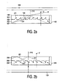
- Figures 4a-4f show further variations of an multi-layered illumination arrangement.
- a first layer in the form of a lightguide substrate 401 receives unpolarized light from a lamp 420.
- the propagation of the light and the separation into the S- and P-component is indicated in each of the figures 4a-4f . Details regarding the propagation have already been presented above in connection with figures 1-3 .
- All examples in figures 4a-4f include a birefringent layer which is provided with a microstructure 410,430.
- the microstructure 410 in the examples of figures 4a-4c are parallel grooves whereas the microstructure 430 in the examples of figures 4d-4f are in the form of parallel ridges.
- Both non-collimated and highly collimated light was coupled into the waveguide and the polarization dependent angular distribution of emitted light was measured.
- the measurements show that light is mainly emitted at an angle of approximately 15 degrees with the normal to the plane of the waveguide.
- the contrast ratio between S- and P-polarized light is low in the case of non-collimated light (1.9 in the direction of the normal 210) and improves upon collimation of the incoming light (2.5 in the direction of the normal 210).
Landscapes
- Physics & Mathematics (AREA)
- General Physics & Mathematics (AREA)
- Optics & Photonics (AREA)
- Nonlinear Science (AREA)
- Mathematical Physics (AREA)
- Chemical & Material Sciences (AREA)
- Crystallography & Structural Chemistry (AREA)
- Polarising Elements (AREA)
- Light Guides In General And Applications Therefor (AREA)
- Liquid Crystal (AREA)
- Planar Illumination Modules (AREA)
- Optical Integrated Circuits (AREA)
Claims (9)
- Beleuchtungsanordnung, die angeordnet ist, um unpolarisiertes Licht mit einer erwünschten und einer unerwünschten Polarisation zu empfangen und polarisiertes Licht der erwünschten Polarisation zu emittieren, mit zumindest einer doppelbrechenden, zweiten Schicht (102) mit Brechungsindizes in der Richtung der erwünschten und unerwünschten Polarisation, wobei die Brechungsindizes in der Richtung der erwünschten und der unerwünschten Polarisation unterschiedlich sind, einer dritten Schicht (103) mit einem, mit dem Brechungsindex der zweiten, doppelbrechenden Schicht (102) in der Richtung der erwünschten Polarisation nicht übereinstimmenden Brechungsindex und einem in der Richtung der unerwünschten Polarisation im Wesentlichen übereinstimmenden Brechungsindex, um zwischen der dritten Schicht (103) und der doppelbrechenden, zweiten Schicht (102) eine polarisationsselektive Grenzfläche (108) vorzusehen, einer ersten Schicht (101) in Form eines optisch klaren Lichtleiters, wobei die erste Schicht (101) mit der dritten Schicht (103) zu einer Einfachschicht zusammengefügt ist oder die erste (101) und die dritte Schicht (103) getrennte Schichten sind und die polarisationsselektive Grenzfläche (108) eine Mikrostruktur (211) umfasst, dadurch gekennzeichnet, dass die Mikrostruktur (211) so aufgebaut ist, dass sie eine Emission von polarisiertem Licht der erwünschten Polarisation entlang der Normalen einer Hauptebene der doppelbrechenden, zweiten Schicht (102) durch selektive, innere Totalreflexion der erwünschten Polarisation an der polarisationsselektiven Grenzfläche (108) erleichtert.
- Anordnung nach Anspruch 1, wobei die doppelbrechende, zweite Schicht (102) zwischen dem Lichtleiter (101) und der dritten Schicht (103) angeordnet ist, wobei die dritte Schicht (103) auf der doppelbrechenden, zweiten Schicht (102) aufgetragen ist.
- Anordnung nach Anspruch 1, wobei die dritte Schicht (423) zwischen dem Lichtleiter (401) und der doppelbrechenden Schicht (422) angeordnet ist, wobei die dritte Schicht (423) den Lichtleiter (401) an der doppelbrechenden, zweiten Schicht (422) hält.
- Anordnung nach einem der Ansprüche 1-3, wobei die Mikrostruktur (430) sich aus der doppelbrechenden, zweiten Schicht (432) erstreckende Grate umfasst.
- Anordnung nach einem der Ansprüche 1-3, wobei die Mikrostruktur (410) sich in die doppelbrechende, zweite Schicht (402) erstreckende Rillen umfasst.
- Anordnung nach einem der Ansprüche 1-5, wobei die dritte Schicht (103) ein isotropes Material mit einem, einem der Brechungsindizes der doppelbrechenden Schicht (102) im Wesentlichen entsprechenden Brechungsindex ist.
- Anordnung nach einem der Ansprüche 1-6, wobei der Lichtleiter (101) einen Brechungsindex aufweist, der geringer als die Brechungsindizes der doppelbrechenden Schicht (102) ist.
- Anordnung nach einem der Ansprüche 1-6, wobei der Lichtleiter (101) einen Brechungsindex aufweist, der zwischen den Brechungsindizes der doppelbrechenden Schicht (102) liegt.
- Displaysystem mit einem Flüssigkristall-Flachdisplay (100) und einer Beleuchtungsanordnung nach einem der Ansprüche 1-8.
Priority Applications (1)
| Application Number | Priority Date | Filing Date | Title |
|---|---|---|---|
| EP02765193A EP1432948B1 (de) | 2001-09-26 | 2002-09-06 | Mikrostrukturiertes beleuchtungssystem zur bereitstellung polarisierten lichtes |
Applications Claiming Priority (4)
| Application Number | Priority Date | Filing Date | Title |
|---|---|---|---|
| EP01203674 | 2001-09-26 | ||
| EP01203674 | 2001-09-26 | ||
| PCT/IB2002/003660 WO2003027568A1 (en) | 2001-09-26 | 2002-09-06 | Micro-structured illumination system for providing polarized light |
| EP02765193A EP1432948B1 (de) | 2001-09-26 | 2002-09-06 | Mikrostrukturiertes beleuchtungssystem zur bereitstellung polarisierten lichtes |
Publications (2)
| Publication Number | Publication Date |
|---|---|
| EP1432948A1 EP1432948A1 (de) | 2004-06-30 |
| EP1432948B1 true EP1432948B1 (de) | 2009-11-11 |
Family
ID=8180978
Family Applications (1)
| Application Number | Title | Priority Date | Filing Date |
|---|---|---|---|
| EP02765193A Expired - Lifetime EP1432948B1 (de) | 2001-09-26 | 2002-09-06 | Mikrostrukturiertes beleuchtungssystem zur bereitstellung polarisierten lichtes |
Country Status (8)
| Country | Link |
|---|---|
| US (1) | US7265800B2 (de) |
| EP (1) | EP1432948B1 (de) |
| JP (1) | JP4437920B2 (de) |
| KR (1) | KR100905100B1 (de) |
| CN (1) | CN100564998C (de) |
| AT (1) | ATE448442T1 (de) |
| DE (1) | DE60234365D1 (de) |
| WO (1) | WO2003027568A1 (de) |
Families Citing this family (90)
| Publication number | Priority date | Publication date | Assignee | Title |
|---|---|---|---|---|
| AU2001227959A1 (en) * | 2000-01-19 | 2001-07-31 | Omlidon Technologies Llc | Polarizing device |
| WO2004070464A1 (en) * | 2003-02-10 | 2004-08-19 | Koninklijke Philips Electronics N.V. | Display illumination system and manufacturing method thereof |
| US7510316B2 (en) * | 2003-07-14 | 2009-03-31 | Koninklijke Philips Electronics N.V. | Ultra compact illumination system for display systems |
| GB0322682D0 (en) * | 2003-09-27 | 2003-10-29 | Koninkl Philips Electronics Nv | Backlight for 3D display device |
| US7163149B2 (en) * | 2004-03-02 | 2007-01-16 | Symbol Technologies, Inc. | System and method for illuminating and reading optical codes imprinted or displayed on reflective surfaces |
| KR100819650B1 (ko) * | 2004-03-18 | 2008-04-07 | 샤프 가부시키가이샤 | 액정 표시 패널 및 액정 표시 장치 |
| WO2006026743A1 (en) * | 2004-08-31 | 2006-03-09 | Fusion Optix, Inc. | Enhanced light diffusing sheet |
| DE602005016007D1 (de) * | 2004-11-18 | 2009-09-24 | Koninkl Philips Electronics Nv | Anzeige für zwei- und dreidimensionale ansicht |
| US20060138686A1 (en) * | 2004-12-23 | 2006-06-29 | Ouderkirk Andrew J | Method of making a uniaxially stretched polymeric film having structured surface |
| US20060204720A1 (en) * | 2004-12-23 | 2006-09-14 | Biernath Rolf W | Uniaxially oriented birefringent article having a structured surface |
| US20060138702A1 (en) * | 2004-12-23 | 2006-06-29 | Biernath Rolf W | Method of making uniaxially oriented articles having structured surfaces |
| US20060141219A1 (en) * | 2004-12-23 | 2006-06-29 | Benson Olester Jr | Roll of a uniaxially oriented article having a structured surface |
| US20060141220A1 (en) * | 2004-12-23 | 2006-06-29 | Merrill William W | Uniaxially oriented article having a structured surface |
| US20060141218A1 (en) * | 2004-12-23 | 2006-06-29 | Biernath Rolf W | Uniaxially oriented articles having structured surface |
| US20060138694A1 (en) * | 2004-12-23 | 2006-06-29 | Biernath Rolf W | Method of making a polymeric film having structured surfaces via replication |
| US20060138705A1 (en) * | 2004-12-23 | 2006-06-29 | Korba Gary A | Method of making a structured surface article |
| JP4742596B2 (ja) * | 2005-01-27 | 2011-08-10 | ソニー株式会社 | バックライトユニットおよび液晶表示装置 |
| DE602006009090D1 (de) * | 2005-04-08 | 2009-10-22 | 3M Innovative Properties Co | Strukturierte orientierte filme zur verwendung in displays |
| KR101093227B1 (ko) * | 2005-04-15 | 2011-12-13 | 삼성전자주식회사 | 도광판, 이의 제조 방법, 이를 갖는 백라이트 어셈블리 및이를 갖는 표시장치 |
| JP2008542991A (ja) * | 2005-05-27 | 2008-11-27 | コーニンクレッカ フィリップス エレクトロニクス エヌ ヴィ | ディスプレイ用の照明装置及びその製造方法 |
| JP2008546139A (ja) * | 2005-05-27 | 2008-12-18 | コーニンクレッカ フィリップス エレクトロニクス エヌ ヴィ | 照明装置 |
| KR20060130999A (ko) * | 2005-06-14 | 2006-12-20 | 삼성전자주식회사 | 개선된 도광판, 도광판을 개선한 백라이트 어셈블리 및이를 구비한 표시 장치 |
| WO2007002317A1 (en) * | 2005-06-23 | 2007-01-04 | Fusion Optix, Inc. | Enhanced diffusing plates, films and backlights |
| US20060291214A1 (en) * | 2005-06-23 | 2006-12-28 | Thomas Tessnow | Replaceable vehicle lamp with LED light sources |
| US20070065636A1 (en) * | 2005-08-04 | 2007-03-22 | Merrill William W | Article having a birefringent surface and microstructured features having a variable pitch or angles and process for making the article |
| US7418202B2 (en) * | 2005-08-04 | 2008-08-26 | 3M Innovative Properties Company | Article having a birefringent surface and microstructured features having a variable pitch or angles for use as a blur filter |
| KR100657968B1 (ko) * | 2005-08-27 | 2006-12-14 | 삼성전자주식회사 | 평판표시장치용 조명장치 |
| EP1760500A3 (de) * | 2005-09-02 | 2007-08-01 | Samsung Electronics Co., Ltd. | Beleuchter für ein Flachbildschirmgerät und Beleuchter für ein doppelseitiges Flachbildschirmgerät |
| JP4158824B2 (ja) * | 2005-09-15 | 2008-10-01 | ソニー株式会社 | 光透過フィルム、光透過フィルムの製造方法及び液晶表示装置 |
| WO2007036877A2 (en) * | 2005-09-30 | 2007-04-05 | Koninklijke Philips Electronics N.V. | Back light unit |
| KR100738104B1 (ko) * | 2006-02-08 | 2007-07-12 | 삼성전자주식회사 | 편광 도광판 및 그 제조 방법 및 상기 편광 도광판을이용한 평판표시장치용 조명장치 |
| KR100813253B1 (ko) * | 2006-04-27 | 2008-03-13 | 삼성전자주식회사 | 고효율의 편광도광판 유닛, 이를 채용한 백라이트 유닛 및디스플레이 장치 |
| KR100813255B1 (ko) * | 2006-06-02 | 2008-03-13 | 삼성전자주식회사 | 고출력 도광판 및 이를 채용한 백라이트 유닛 |
| KR100837398B1 (ko) * | 2006-06-14 | 2008-06-12 | 삼성전자주식회사 | 편광분리박막 및 이를 채용한 백라이트 유닛 |
| US9134471B2 (en) * | 2006-06-28 | 2015-09-15 | 3M Innovative Properties Company | Oriented polymeric articles and method |
| US20080089093A1 (en) * | 2006-10-17 | 2008-04-17 | Miller Anne M | Backlight unit using particular direct backlight assembly |
| KR100785025B1 (ko) * | 2006-10-26 | 2007-12-12 | 삼성전자주식회사 | 디스플레이 소자용 양면 조명장치 및 이를 채용한 양면디스플레이 소자 |
| GB2444081B (en) * | 2006-11-24 | 2011-05-11 | Ocuity Ltd | Manufacture of a birefringent liquid crystal component |
| KR101407292B1 (ko) * | 2007-06-08 | 2014-06-16 | 엘지디스플레이 주식회사 | 백라이트 유닛 |
| US7379130B1 (en) | 2007-10-03 | 2008-05-27 | Vitera Llc | LCD with hetero polar light guide |
| CN102047155B (zh) * | 2008-05-28 | 2013-04-03 | 高通Mems科技公司 | 具有光转向微结构的光导面板、其制造方法和显示装置 |
| KR20160105527A (ko) | 2008-07-10 | 2016-09-06 | 쓰리엠 이노베이티브 프로퍼티즈 컴파니 | 점탄성 도광체 |
| CN107037526A (zh) | 2008-08-08 | 2017-08-11 | 3M创新有限公司 | 具有粘弹性层的用于控制光的光导 |
| US20100135038A1 (en) * | 2008-11-30 | 2010-06-03 | Handschy Mark A | Frontlights for reflective displays |
| TWI357481B (en) * | 2008-12-05 | 2012-02-01 | Ind Tech Res Inst | A light source module for producing polarized ligh |
| KR101518734B1 (ko) * | 2008-12-23 | 2015-05-12 | 삼성전자주식회사 | 편광된 광을 제공하는 백라이트 유닛 및 이를 채용한 디스플레이 장치 |
| JP5084769B2 (ja) * | 2009-03-13 | 2012-11-28 | 株式会社ジャパンディスプレイイースト | 液晶表示装置 |
| US20100302218A1 (en) | 2009-05-29 | 2010-12-02 | Qualcomm Mems Technologies, Inc. | Illumination devices and methods of fabrication thereof |
| KR101104141B1 (ko) * | 2009-11-30 | 2012-01-13 | 한국과학기술원 | 도광 플레이트 및 백라이트 유닛 |
| US9244206B2 (en) * | 2009-12-17 | 2016-01-26 | 3M Innovative Properties Company | Light redirecting film laminate |
| KR101822672B1 (ko) | 2010-01-13 | 2018-01-26 | 쓰리엠 이노베이티브 프로퍼티즈 컴파니 | 점탄성 도광체를 구비한 조명 장치 |
| US9128220B2 (en) * | 2010-11-29 | 2015-09-08 | Sharp Kabushiki Kaisha | Light guide body with continuously variable refractive index, and devices using such body |
| KR101793275B1 (ko) * | 2011-03-24 | 2017-11-03 | 삼성디스플레이 주식회사 | 백라이트 유닛 및 백라이트 유닛을 포함하는 표시장치 |
| JP5649526B2 (ja) | 2011-07-01 | 2015-01-07 | 株式会社ジャパンディスプレイ | 表示装置 |
| TWI450201B (zh) * | 2011-08-05 | 2014-08-21 | Gingy Technology Inc | 指壓板 |
| KR101299453B1 (ko) * | 2011-09-19 | 2013-08-22 | 삼성전자주식회사 | 디스플레이장치 |
| US9004726B2 (en) | 2011-10-27 | 2015-04-14 | Svv Technology Innovations, Inc. | Light directing films |
| CN104884979B (zh) * | 2011-11-14 | 2019-03-01 | 3M创新有限公司 | 用于控制光学膜中的色斑的方法 |
| JP2013246407A (ja) * | 2012-05-29 | 2013-12-09 | Dainippon Printing Co Ltd | 光学シートおよび表示装置 |
| US9829604B2 (en) * | 2012-12-20 | 2017-11-28 | 3M Innovative Properties Company | Method of making multilayer optical film comprising layer-by-layer self-assembled layers and articles |
| US10436969B2 (en) | 2013-01-30 | 2019-10-08 | Ideal Industries Lighting Llc | Optical waveguide and luminaire incorporating same |
| US9442243B2 (en) | 2013-01-30 | 2016-09-13 | Cree, Inc. | Waveguide bodies including redirection features and methods of producing same |
| US9625638B2 (en) | 2013-03-15 | 2017-04-18 | Cree, Inc. | Optical waveguide body |
| US9690029B2 (en) | 2013-01-30 | 2017-06-27 | Cree, Inc. | Optical waveguides and luminaires incorporating same |
| US9869432B2 (en) | 2013-01-30 | 2018-01-16 | Cree, Inc. | Luminaires using waveguide bodies and optical elements |
| US9366396B2 (en) | 2013-01-30 | 2016-06-14 | Cree, Inc. | Optical waveguide and lamp including same |
| US9291320B2 (en) | 2013-01-30 | 2016-03-22 | Cree, Inc. | Consolidated troffer |
| DE102013204442A1 (de) | 2013-03-14 | 2014-10-02 | Carl Zeiss Smt Gmbh | Optischer Wellenleiter zur Führung von Beleuchtungslicht |
| US10400984B2 (en) | 2013-03-15 | 2019-09-03 | Cree, Inc. | LED light fixture and unitary optic member therefor |
| US10379278B2 (en) * | 2013-03-15 | 2019-08-13 | Ideal Industries Lighting Llc | Outdoor and/or enclosed structure LED luminaire outdoor and/or enclosed structure LED luminaire having outward illumination |
| US10209429B2 (en) | 2013-03-15 | 2019-02-19 | Cree, Inc. | Luminaire with selectable luminous intensity pattern |
| US10436970B2 (en) | 2013-03-15 | 2019-10-08 | Ideal Industries Lighting Llc | Shaped optical waveguide bodies |
| US10502899B2 (en) * | 2013-03-15 | 2019-12-10 | Ideal Industries Lighting Llc | Outdoor and/or enclosed structure LED luminaire |
| US9366799B2 (en) | 2013-03-15 | 2016-06-14 | Cree, Inc. | Optical waveguide bodies and luminaires utilizing same |
| US9920901B2 (en) | 2013-03-15 | 2018-03-20 | Cree, Inc. | LED lensing arrangement |
| US9798072B2 (en) | 2013-03-15 | 2017-10-24 | Cree, Inc. | Optical element and method of forming an optical element |
| US9645303B2 (en) | 2013-03-15 | 2017-05-09 | Cree, Inc. | Luminaires utilizing edge coupling |
| US20140347571A1 (en) * | 2013-05-24 | 2014-11-27 | Raytheon Company | Low profile backlight apparatus for high-brightness microdisplays |
| TWI468731B (zh) * | 2014-02-06 | 2015-01-11 | Benq Materials Corp | 光切換模組 |
| TWI479194B (zh) * | 2014-02-06 | 2015-04-01 | Benq Materials Corp | 光切換模組 |
| JP6671940B2 (ja) | 2015-12-07 | 2020-03-25 | 株式会社ジャパンディスプレイ | 表示装置 |
| US11719882B2 (en) | 2016-05-06 | 2023-08-08 | Ideal Industries Lighting Llc | Waveguide-based light sources with dynamic beam shaping |
| US10416377B2 (en) | 2016-05-06 | 2019-09-17 | Cree, Inc. | Luminaire with controllable light emission |
| CN108303812B (zh) * | 2017-01-12 | 2019-11-05 | 江苏集萃智能液晶科技有限公司 | 一种具有调光功能的后视镜 |
| JP2018113225A (ja) * | 2017-01-13 | 2018-07-19 | 大日本印刷株式会社 | 導光板、面光源装置、表示装置 |
| CN110678800B (zh) | 2017-03-21 | 2023-08-25 | 奇跃公司 | 用于照射空间光调制器的方法、设备和系统 |
| CN109307903B (zh) * | 2017-07-28 | 2020-05-12 | 江苏集萃智能液晶科技有限公司 | 一种出射偏振光的背光源及其制备方法和液晶显示装置 |
| US10739513B2 (en) | 2018-08-31 | 2020-08-11 | RAB Lighting Inc. | Apparatuses and methods for efficiently directing light toward and away from a mounting surface |
| US10801679B2 (en) | 2018-10-08 | 2020-10-13 | RAB Lighting Inc. | Apparatuses and methods for assembling luminaires |
| IL270991B (en) * | 2019-11-27 | 2020-07-30 | Lumus Ltd | A light guide with an optical element to perform polarization mixing |
Citations (1)
| Publication number | Priority date | Publication date | Assignee | Title |
|---|---|---|---|---|
| WO2001053745A1 (en) * | 2000-01-19 | 2001-07-26 | Omlidon Technologies Llc | Polarizing device |
Family Cites Families (4)
| Publication number | Priority date | Publication date | Assignee | Title |
|---|---|---|---|---|
| JP3521940B2 (ja) * | 1992-10-09 | 2004-04-26 | 旭硝子株式会社 | 照明装置および液晶表示装置 |
| EP0787316B1 (de) | 1995-08-23 | 2004-05-19 | Koninklijke Philips Electronics N.V. | Beleuchtungssystem für eine flachtafel-bildanzeigevorrichtung |
| JP3820623B2 (ja) * | 1996-04-26 | 2006-09-13 | 旭硝子株式会社 | 導光板および液晶表示装置 |
| WO1998012593A1 (en) * | 1996-09-23 | 1998-03-26 | Philips Electronics N.V. | Illumination system for a flat-panel picture display device |
-
2002
- 2002-09-06 EP EP02765193A patent/EP1432948B1/de not_active Expired - Lifetime
- 2002-09-06 KR KR1020047004214A patent/KR100905100B1/ko not_active Expired - Fee Related
- 2002-09-06 WO PCT/IB2002/003660 patent/WO2003027568A1/en not_active Ceased
- 2002-09-06 CN CNB028186737A patent/CN100564998C/zh not_active Expired - Fee Related
- 2002-09-06 DE DE60234365T patent/DE60234365D1/de not_active Expired - Lifetime
- 2002-09-06 JP JP2003531089A patent/JP4437920B2/ja not_active Expired - Fee Related
- 2002-09-06 AT AT02765193T patent/ATE448442T1/de not_active IP Right Cessation
- 2002-09-23 US US10/252,931 patent/US7265800B2/en not_active Expired - Fee Related
Patent Citations (1)
| Publication number | Priority date | Publication date | Assignee | Title |
|---|---|---|---|---|
| WO2001053745A1 (en) * | 2000-01-19 | 2001-07-26 | Omlidon Technologies Llc | Polarizing device |
Also Published As
| Publication number | Publication date |
|---|---|
| EP1432948A1 (de) | 2004-06-30 |
| JP4437920B2 (ja) | 2010-03-24 |
| JP2005504412A (ja) | 2005-02-10 |
| CN1558999A (zh) | 2004-12-29 |
| KR100905100B1 (ko) | 2009-06-30 |
| CN100564998C (zh) | 2009-12-02 |
| US20030058383A1 (en) | 2003-03-27 |
| WO2003027568A1 (en) | 2003-04-03 |
| US7265800B2 (en) | 2007-09-04 |
| ATE448442T1 (de) | 2009-11-15 |
| KR20040047848A (ko) | 2004-06-05 |
| DE60234365D1 (de) | 2009-12-24 |
Similar Documents
| Publication | Publication Date | Title |
|---|---|---|
| US7265800B2 (en) | Micro-structured illumination system for providing polarized light | |
| US6996296B2 (en) | Polarizing device | |
| US7072544B2 (en) | Polarized light-emitting waveguide plate | |
| CN101174060B (zh) | 用于显示装置的双侧照明装置和使用其的双侧显示装置 | |
| US5661839A (en) | Light guide employing multilayer optical film | |
| CN101395509B (zh) | 利用内全反射的偏振转向膜 | |
| JP2002303864A (ja) | 照明装置及び液晶表示装置 | |
| KR20100056984A (ko) | 광학 시트, 조명 장치 및 액정 표시 장치 | |
| JP2008288195A (ja) | 偏光転向フィルムを含む、低減された色分解を有するバックライトユニット | |
| CN1209884A (zh) | 用于平板图像显示设备的照明系统 | |
| EP0953130A4 (de) | Beleuchtungsvorrichtung | |
| WO2002103445A1 (en) | Illuminating device and liquid crystal display device | |
| US20080100913A1 (en) | Polarization separating film and illumination apparatus for display device using the polarization separating film | |
| TWI596390B (zh) | 背光光導 | |
| CN101432640A (zh) | 偏振转向膜 | |
| EP0402146B1 (de) | Prismatische Beleuchtungseinrichtung für flachen Bildschirm | |
| JP2000147429A (ja) | 偏光面光源装置及び液晶表示装置 | |
| JP2001167625A (ja) | 面光源装置及び液晶表示装置 | |
| WO2009100303A1 (en) | Perforated backlight | |
| JP3303278B2 (ja) | 偏光面光源装置及び液晶表示装置 | |
| Jagt et al. | 45.3: Micro‐structured Polymeric Linearly Polarized Light Emitting Lightguide for LCD Illumination | |
| JP2009003412A (ja) | 低減された色分解を有する偏光転向フィルム | |
| JP2009231018A (ja) | 導光板、面光源装置、および液晶表示装置 | |
| TW200916904A (en) | Lightguide lamination to reduce reflector loss | |
| JP2000147488A (ja) | 偏光面光源装置及び液晶表示装置 |
Legal Events
| Date | Code | Title | Description |
|---|---|---|---|
| PUAI | Public reference made under article 153(3) epc to a published international application that has entered the european phase |
Free format text: ORIGINAL CODE: 0009012 |
|
| 17P | Request for examination filed |
Effective date: 20040426 |
|
| AK | Designated contracting states |
Kind code of ref document: A1 Designated state(s): AT BE BG CH CY CZ DE DK EE ES FI FR GB GR IE IT LI LU MC NL PT SE SK TR |
|
| RAP1 | Party data changed (applicant data changed or rights of an application transferred) |
Owner name: KONINKLIJKE PHILIPS ELECTRONICS N.V. |
|
| 17Q | First examination report despatched |
Effective date: 20060929 |
|
| 17Q | First examination report despatched |
Effective date: 20060929 |
|
| GRAP | Despatch of communication of intention to grant a patent |
Free format text: ORIGINAL CODE: EPIDOSNIGR1 |
|
| GRAS | Grant fee paid |
Free format text: ORIGINAL CODE: EPIDOSNIGR3 |
|
| GRAA | (expected) grant |
Free format text: ORIGINAL CODE: 0009210 |
|
| AK | Designated contracting states |
Kind code of ref document: B1 Designated state(s): AT BE BG CH CY CZ DE DK EE ES FI FR GB GR IE IT LI LU MC NL PT SE SK TR |
|
| REG | Reference to a national code |
Ref country code: GB Ref legal event code: FG4D |
|
| REG | Reference to a national code |
Ref country code: CH Ref legal event code: EP |
|
| REG | Reference to a national code |
Ref country code: IE Ref legal event code: FG4D |
|
| REF | Corresponds to: |
Ref document number: 60234365 Country of ref document: DE Date of ref document: 20091224 Kind code of ref document: P |
|
| NLV1 | Nl: lapsed or annulled due to failure to fulfill the requirements of art. 29p and 29m of the patents act | ||
| PG25 | Lapsed in a contracting state [announced via postgrant information from national office to epo] |
Ref country code: PT Free format text: LAPSE BECAUSE OF FAILURE TO SUBMIT A TRANSLATION OF THE DESCRIPTION OR TO PAY THE FEE WITHIN THE PRESCRIBED TIME-LIMIT Effective date: 20100311 Ref country code: ES Free format text: LAPSE BECAUSE OF FAILURE TO SUBMIT A TRANSLATION OF THE DESCRIPTION OR TO PAY THE FEE WITHIN THE PRESCRIBED TIME-LIMIT Effective date: 20100222 Ref country code: SE Free format text: LAPSE BECAUSE OF FAILURE TO SUBMIT A TRANSLATION OF THE DESCRIPTION OR TO PAY THE FEE WITHIN THE PRESCRIBED TIME-LIMIT Effective date: 20091111 Ref country code: FI Free format text: LAPSE BECAUSE OF FAILURE TO SUBMIT A TRANSLATION OF THE DESCRIPTION OR TO PAY THE FEE WITHIN THE PRESCRIBED TIME-LIMIT Effective date: 20091111 |
|
| PG25 | Lapsed in a contracting state [announced via postgrant information from national office to epo] |
Ref country code: CY Free format text: LAPSE BECAUSE OF FAILURE TO SUBMIT A TRANSLATION OF THE DESCRIPTION OR TO PAY THE FEE WITHIN THE PRESCRIBED TIME-LIMIT Effective date: 20091111 |
|
| PG25 | Lapsed in a contracting state [announced via postgrant information from national office to epo] |
Ref country code: AT Free format text: LAPSE BECAUSE OF FAILURE TO SUBMIT A TRANSLATION OF THE DESCRIPTION OR TO PAY THE FEE WITHIN THE PRESCRIBED TIME-LIMIT Effective date: 20091111 Ref country code: BE Free format text: LAPSE BECAUSE OF FAILURE TO SUBMIT A TRANSLATION OF THE DESCRIPTION OR TO PAY THE FEE WITHIN THE PRESCRIBED TIME-LIMIT Effective date: 20091111 |
|
| PG25 | Lapsed in a contracting state [announced via postgrant information from national office to epo] |
Ref country code: EE Free format text: LAPSE BECAUSE OF FAILURE TO SUBMIT A TRANSLATION OF THE DESCRIPTION OR TO PAY THE FEE WITHIN THE PRESCRIBED TIME-LIMIT Effective date: 20091111 Ref country code: DK Free format text: LAPSE BECAUSE OF FAILURE TO SUBMIT A TRANSLATION OF THE DESCRIPTION OR TO PAY THE FEE WITHIN THE PRESCRIBED TIME-LIMIT Effective date: 20091111 Ref country code: BG Free format text: LAPSE BECAUSE OF FAILURE TO SUBMIT A TRANSLATION OF THE DESCRIPTION OR TO PAY THE FEE WITHIN THE PRESCRIBED TIME-LIMIT Effective date: 20100211 |
|
| PG25 | Lapsed in a contracting state [announced via postgrant information from national office to epo] |
Ref country code: SK Free format text: LAPSE BECAUSE OF FAILURE TO SUBMIT A TRANSLATION OF THE DESCRIPTION OR TO PAY THE FEE WITHIN THE PRESCRIBED TIME-LIMIT Effective date: 20091111 Ref country code: CZ Free format text: LAPSE BECAUSE OF FAILURE TO SUBMIT A TRANSLATION OF THE DESCRIPTION OR TO PAY THE FEE WITHIN THE PRESCRIBED TIME-LIMIT Effective date: 20091111 |
|
| PLBE | No opposition filed within time limit |
Free format text: ORIGINAL CODE: 0009261 |
|
| STAA | Information on the status of an ep patent application or granted ep patent |
Free format text: STATUS: NO OPPOSITION FILED WITHIN TIME LIMIT |
|
| 26N | No opposition filed |
Effective date: 20100812 |
|
| PG25 | Lapsed in a contracting state [announced via postgrant information from national office to epo] |
Ref country code: GR Free format text: LAPSE BECAUSE OF FAILURE TO SUBMIT A TRANSLATION OF THE DESCRIPTION OR TO PAY THE FEE WITHIN THE PRESCRIBED TIME-LIMIT Effective date: 20100212 |
|
| PG25 | Lapsed in a contracting state [announced via postgrant information from national office to epo] |
Ref country code: IT Free format text: LAPSE BECAUSE OF FAILURE TO SUBMIT A TRANSLATION OF THE DESCRIPTION OR TO PAY THE FEE WITHIN THE PRESCRIBED TIME-LIMIT Effective date: 20091111 |
|
| PG25 | Lapsed in a contracting state [announced via postgrant information from national office to epo] |
Ref country code: MC Free format text: LAPSE BECAUSE OF NON-PAYMENT OF DUE FEES Effective date: 20100930 |
|
| REG | Reference to a national code |
Ref country code: CH Ref legal event code: PL |
|
| GBPC | Gb: european patent ceased through non-payment of renewal fee |
Effective date: 20100906 |
|
| REG | Reference to a national code |
Ref country code: FR Ref legal event code: ST Effective date: 20110531 |
|
| REG | Reference to a national code |
Ref country code: DE Ref legal event code: R119 Ref document number: 60234365 Country of ref document: DE Effective date: 20110401 |
|
| PG25 | Lapsed in a contracting state [announced via postgrant information from national office to epo] |
Ref country code: DE Free format text: LAPSE BECAUSE OF NON-PAYMENT OF DUE FEES Effective date: 20110401 Ref country code: LI Free format text: LAPSE BECAUSE OF NON-PAYMENT OF DUE FEES Effective date: 20100930 Ref country code: FR Free format text: LAPSE BECAUSE OF NON-PAYMENT OF DUE FEES Effective date: 20100930 Ref country code: CH Free format text: LAPSE BECAUSE OF NON-PAYMENT OF DUE FEES Effective date: 20100930 Ref country code: IE Free format text: LAPSE BECAUSE OF NON-PAYMENT OF DUE FEES Effective date: 20100906 |
|
| PG25 | Lapsed in a contracting state [announced via postgrant information from national office to epo] |
Ref country code: GB Free format text: LAPSE BECAUSE OF NON-PAYMENT OF DUE FEES Effective date: 20100906 |
|
| PG25 | Lapsed in a contracting state [announced via postgrant information from national office to epo] |
Ref country code: LU Free format text: LAPSE BECAUSE OF NON-PAYMENT OF DUE FEES Effective date: 20100906 Ref country code: NL Free format text: LAPSE BECAUSE OF FAILURE TO SUBMIT A TRANSLATION OF THE DESCRIPTION OR TO PAY THE FEE WITHIN THE PRESCRIBED TIME-LIMIT Effective date: 20091111 |
|
| PG25 | Lapsed in a contracting state [announced via postgrant information from national office to epo] |
Ref country code: TR Free format text: LAPSE BECAUSE OF FAILURE TO SUBMIT A TRANSLATION OF THE DESCRIPTION OR TO PAY THE FEE WITHIN THE PRESCRIBED TIME-LIMIT Effective date: 20091111 |