EP1433069B1 - Bussytem und busschnittstelle zum anschliessen an einen bus - Google Patents
Bussytem und busschnittstelle zum anschliessen an einen bus Download PDFInfo
- Publication number
- EP1433069B1 EP1433069B1 EP02765263A EP02765263A EP1433069B1 EP 1433069 B1 EP1433069 B1 EP 1433069B1 EP 02765263 A EP02765263 A EP 02765263A EP 02765263 A EP02765263 A EP 02765263A EP 1433069 B1 EP1433069 B1 EP 1433069B1
- Authority
- EP
- European Patent Office
- Prior art keywords
- bus
- processor
- station
- bus interface
- usb
- Prior art date
- Legal status (The legal status is an assumption and is not a legal conclusion. Google has not performed a legal analysis and makes no representation as to the accuracy of the status listed.)
- Expired - Lifetime
Links
Images



Classifications
-
- G—PHYSICS
- G06—COMPUTING OR CALCULATING; COUNTING
- G06F—ELECTRIC DIGITAL DATA PROCESSING
- G06F13/00—Interconnection of, or transfer of information or other signals between, memories, input/output devices or central processing units
- G06F13/14—Handling requests for interconnection or transfer
-
- G—PHYSICS
- G06—COMPUTING OR CALCULATING; COUNTING
- G06F—ELECTRIC DIGITAL DATA PROCESSING
- G06F13/00—Interconnection of, or transfer of information or other signals between, memories, input/output devices or central processing units
- G06F13/14—Handling requests for interconnection or transfer
- G06F13/20—Handling requests for interconnection or transfer for access to input/output bus
- G06F13/24—Handling requests for interconnection or transfer for access to input/output bus using interrupt
-
- G—PHYSICS
- G06—COMPUTING OR CALCULATING; COUNTING
- G06F—ELECTRIC DIGITAL DATA PROCESSING
- G06F13/00—Interconnection of, or transfer of information or other signals between, memories, input/output devices or central processing units
- G06F13/38—Information transfer, e.g. on bus
- G06F13/42—Bus transfer protocol, e.g. handshake; Synchronisation
- G06F13/4247—Bus transfer protocol, e.g. handshake; Synchronisation on a daisy chain bus
- G06F13/426—Bus transfer protocol, e.g. handshake; Synchronisation on a daisy chain bus using an embedded synchronisation, e.g. Firewire bus, Fibre Channel bus, SSA bus
Definitions
- the invention relates to a bus system comprising a first station and a second station coupled by a bus for transferring data and control signals, said bus being conceived to operate according to a protocol in which said first station repeatedly sends requests to said second station.
- the invention also relates to a bus interface, comprising a connection for a bus and an input for receiving request properties from a processor.
- USB specification is a standard promulgated by a group of companies including Compaq Computer Corporation, Hewlett-Packard Company, Intel Corporation, Lucent Technologies Inc, Microsoft Corporation, NEC Corporation, and Koninklijke Philips Electronics N.V. Described below are various aspects of the USB relevant to a complete understanding of the present invention. Further background concerning the USB may be obtained from USB Specification, Revision 2.0.
- the USB is a standard bus designed to support data exchange between a personal computer and a wide variety of peripherals such as webcams, printers, scanners, microphones and keyboards.
- the USB thus replaces existing interfaces such as the RS-232C serial ports, parallel ports, and PS/2 interfaces.
- Further developments of the USB aim at bus systems where another apparatus replaces the personal computer.
- Such an apparatus could be, for example, a digital still camera, a video camera, a personal digital assistant, or a cellular phone.
- USB stations are defined as hosts (e.g. personal computers) and as devices (peripherals). In general there is only one host on any USB system.
- a USB interface at the host is also referred to as a host controller.
- the host controller may be implemented in a combination of hardware, firmware, or software.
- USB devices are defined as hubs which provide additional attachment points or functions which provide capabilities to the system. The devices are connected to the host via a tiered-star topology. Hubs indicate the attachment or removal of a USB device.
- the host determines if a newly attached USB device is a hub or a function and assigns a unique USB address to the USB device. All USB devices are accessed by a unique USB address. Each device additionally supports one or more endpoints with which the host may communicate. The following description will be limited to USB devices defined as functions.
- the USB is a polled bus.
- the host controller initiates all data transfers. Most bus transactions involve the transmission of up to three packets. Each transaction begins when the host controller, on a scheduled basis, sends a USB packet describing the type and direction of the transaction, the USB device address, and endpoint number. This packet is referred to as the "token packet".
- the USB device that is addressed selects itself by decoding the appropriate address fields.
- data is transferred either from the host to a device or from a device to the host.
- the direction of data transfer is specified in the token packet.
- the source of the transaction then sends a data packet or indicates it has no data to transfer.
- the destination in general, responds with a handshake packet indicating whether the transfer was successful.
- the USB architecture comprehends three basic types of data transfer: (1) isochronous transfers: periodic, continuous communication between host and device, typically used for time-relevant information, which occupies a pre-negotiated amount of USB bandwidth with a pre-negotiated latency; (2) interrupt transfers: low-frequency, bounded latency communication, typically used for asynchronous data such as characters or coordinates with human perceptible echo or feedback response characteristics, and; (3) bulk transfers: non-periodic, large-packet bursty communication, typically used for data that can use any available bandwidth and can also be delayed until bandwidth is available.
- both types of bus station, host and device comprise a processor or computing system to either process or generate data or to control the flow of data or both.
- a straightforward implementation of a USB system as described above could lead to a significant overhead for both the processor in the bus station acting as a host and the processor in the bus station acting as a device. This holds especially for the interrupt transfers.
- the host Due to the polled nature of the bus system, the host needs to interrogate the involved device, for instance a keyboard, on a regular basis.
- the invention provides a bus system as defined in the opening paragraph, wherein said first station comprises a processor, a bus interface, and a buffer coupled to said interruptible processor and said bus interface, where
- the processor within the first station needs to provide information to the second station or needs to obtain information from the second station.
- the first station needs to communicate with the second station.
- a polled bus system such as a USB system
- the communication is initiated by the first station, being a host in a USB system.
- the second station being a device in a USB system
- the second station is only capable of receiving or providing data on an irregular basis, it happens frequently that the first station needs to poll the second station quite a number of times before a successful transfer of information takes place. In other words under these circumstances the first station needs to re-send the same request relatively often to the second station before a successful transfer of information takes place.
- said processor would need to prepare said request every time it needs to be send and said bus interface would then actually send said request via said bus to said second station.
- the processor generates or determines the properties of the request. By enhancing the capabilities of the bus interface, said bus interface can actually generate the request out of said properties provided by the processor and send the request over the bus to said second station as many times as is required.
- the bus system according to the invention also comprises a buffer within the first station that is used to store the request properties provided by the processor.
- the buffer is preferably accessible for both the processor and the bus interface. In this way the communication overhead of the processor is reduced.
- US-A-6145045 discloses an apparatus for a method of sending data on a USB using a memory shared among a number of end points.
- the processor may have information on the characteristics of the second station that can be used to adjust the polling rate of the bus interface. For instance, a USB system establishes a time base of either 1 millisecond, called a frame, or of 125 microsecond, called a microframe. If the polling rate information were not included in the request properties, the bus interface would use a fixed polling rate, presumably sending a request at the maximum polling rate of once per (micro) frame. The polling rate information being included in the request properties, the bus interface adjusts the polling rate as needed, using low polling rates whenever possible and high polling rates when required. Bus load and communication overhead for the second station are thus reduced.
- the request itself may, but does not necessarily, contain a payload, i. e. a data item.
- a payload i. e. a data item.
- a further embodiment of the bus system according to the invention is characterized in that said second station responds to said requests, that said processor is an interruptible processor and said bus interface is operable for interrupting said processor upon reception of selected responses of said second station. It is not necessary to interrupt said processor if no further action is required. Thus it is not necessary to report back the result of the communication with the second station if either the communication is completed as expected or if no new information, no data items, are provided by the second station. For example, in USB system the second station may respond by sending a message with a data item acknowledge signal, a negative acknowledge signal, by sending a signal to indicate it is stalled.
- the second station does not respond by sending a signal, or if no signal is received by the first station due to an error in the communication between the first station and the second station, this may be interpreted as a response too.
- the selected responses may comprise the absence of a response signal from the second station.
- Communication overhead of the processor is further reduced if the processor is only interrupted upon reception of the responses that require further action by the processor. To this end the bus interface selects those responses out of the received responses. Programmed to handle such situations the processor can decide upon necessary further actions.
- a bus interface comprises a connection for a bus and an input for receiving request properties from an interruptible processor and is characterized in that it comprises a buffer operable to store said request properties and a controller operable to generate requests out of the stored request properties and to repeatedly send said requests to the connection.
- Fig. 1 is a diagram showing the interrupt transaction format as specified in the USB specification, revision 2.0.
- All USB devices are accessed by a unique USB address.
- Each device additionally supports one or more endpoints with which the host may communicate.
- USB supports functional data and control exchange between the USB host and USB devices.
- USB data transfers take place between host software and a particular endpoint on a USB device.
- the USB architecture comprehends three basic types of transfer:
- Bus transactions including data transfers generally involve three stages: a Setup stage 102, a Data stage 103, and a Status stage 104.
- Bus transactions including data transfers generally involve the transmission of three different packets, e.g. a Token packet 105, 106, a Data packet 107, 108, and a Handshake packet 109, 110, 111, 112, 115, 116.
- a Token packet 105, 106 e.g. a Token packet 105, 106, a Data packet 107, 108, and a Handshake packet 109, 110, 111, 112, 115, 116.
- Interrupt transactions may consist of IN transfers or OUT transfers.
- the USB host will start the transaction by sending an IN token 105.
- a USB device may return data 107, a negative acknowledge signal (NAK) 111, or a signal indicating the USB device is unable to complete a command (STALL) 112. If the endpoint has no new interrupt information to return (i.e. no interrupt is pending), the USB device returns a NAK handshake 111 during the Data stage 103. If the USB device is unable to complete a command, the USB device returns a STALL handshake 112. If an interrupt is pending, the USB device returns the interrupt information as a Data packet 107.
- NAK negative acknowledge signal
- STALL signal indicating the USB device is unable to complete a command
- the USB host in response to receipt of the Data packet 107 issues either an ACK handshake 109 (acknowledge signal) if the data was received error-free or returns no handshake, indicated by line 113, if the Data packet 107 was received corrupted. Furthermore the USB host will not issue an ACK 109 in case no response to the IN token 105 is received at all from the USB device. This situation is indicated by line 114. After completion of the IN transfer, the USB system returns to the Idle mode 101.
- ACK handshake 109 acknowledge signal
- the USB host will start the transaction by sending an OUT token 106. This is followed by sending a Data packet 108.
- the USB device may issue in the Status stage 104 an ACK handshake 110 if the data was received error free, a NAK handshake 115 indicating the device is not able to process the data, or a STALL handshake 116 indicating the USB device is currently stalled.
- the USB device returns no handshake, indicated by line 117, if the Data packet 107 was received corrupted.
- the USB device will not issue an ACK handshake 110 in case it does not receive data from the USB host, a situation indicated by line 118. After completion of the OUT transfer the USB system returns to the Idle mode 101.
- All packets begin with a SYNC field, which is used by input circuitry to align incoming data with a local clock.
- a packet identifier (PID) immediately follows the SYNC field of every USB packet.
- the PID consists of a four-bit ID field followed by a four-bit check field.
- the PID indicates the type of packet (e.g. Token 105, 106, Data 107, 108, and Handshake 109, 110, 111, 112, 115, 116) and the format of the packet along with the type of variant detection applied to the packet.
- the four-bit check field of the PID ensures reliable decoding.
- a Token packet 105, 106 includes an ADDR field which specifies the target USB device, via its USB address, that is the source or destination of a Data packet 107, 108, depending on the value of the Token PID. USB devices must perform a complete decoding of the ADDR field.
- a Data packet 107, 108 includes a data field which may range from zero to N bytes and must amount to integral numbers of bytes. Data bits within each byte are shifted out most significant bit first.
- the data field of a Data packet is divided into fields which give extra information to the USB device regarding the request being made.
- One field, the command code tells what the targeted USB device should do, such as set up a read from a USB device space or set up a write to a USB device space.
- the read space command is used to request information from a given location in a given space of a USB device.
- the command is used to set up the read, which is followed by a request from the host for the USB device to send data.
- the USB device then sends the data it has retrieved from the previously specified space.
- the write space uses exactly the same definition as the read space. However, the Data packet contains data transferred by the host to the USB device.
- a Handshake packet 109, 110, 111, 112, 115, 116 consists of only a PID. As indicated above, Handshake packets are used to report the status of a data transfer and can return values indicating successful reception of data, CRC failure, flow control, and certain fault conditions.
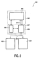
- Fig. 2 is a block diagram showing a bus system according to the invention.
- the bus system 201 comprises a first station 202, acting as a USB host, and second stations 203 and 204, acting as USB devices.
- the stations 202, 203, 204 are coupled by bus connections 205.
- the first station 202 is shown in more detail. It comprises an interruptible processor 206 and a bus interface 207.
- the bus interface comprises a buffer 208 and a controller 209. It is not necessary that the buffer is part of the bus interface. In an alternative arrangement the buffer could be placed within the first station 202, but outside the bus interface.
- Both the processor 206 and the controller 209 have access to the buffer 208.
- the controller is coupled to the bus connections 205. Furthermore the controller 209 has an interrupt connection 210 to the processor 206.
- Fig. 3A is a message diagram showing transactions for data transmission.
- the message diagram illustrates the operation of the system of Fig. 1 for interrupt transactions consisting of IN transfers. Going top-down the time increases.
- Information exchange between the processor 206 and the bus interface 207 is symbolized by arrows between a first line 301 and a second line 302.
- Information exchange between the bus interface and the second station 203, 204 is symbolized by arrows between the second line 302 and a third line 303.
- the processor 206 requires data from one of the second stations 203, 204, a USB device.
- the bus interface 207 should repeatedly issue a request for data to the bus connections 205. To reduce the communication overhead for the processor it should be sufficient to have the processor provide the request properties only once. If the addressed USB device returns data, the bus interface 207 should interrupt the processor via the interrupt connection and provide the processor with the data. In case an error occurs the processor should also be notified. In these situations the bus interface 207 should apply an interrupt to the processor too. In other situations no action is required from the processor, so that the bus interface 207 should not interrupt the processor.
- the processor 206 in a message 309 sends the request properties to the bus interface 207, where the request properties are stored in the buffer. Based on the request properties within the message 309, which are retrieved from the buffer, the bus interface 207 initiates the IN transfer by issuing an IN token 310 on the bus. The second station, the addressed USB device, responds by sending a message 311 with a data item. Upon reception of this message the bus interface 207 sends an interrupt signal 312 via the interrupt connection 210, to the processor 206 to inform the processor 206 that new data is available. Furthermore, it issues an Acknowledge signal 313 to the addressed USB device. This completes the IN transfer 304.
- the bus interface 207 again retrieves the request properties from the buffer, while no new information is required from the processor 206.
- the bus interface 207 initiates the IN transfer by issuing an IN token 314 on the bus.
- the addressed USB device responds by sending a message 315 with a data item. Due to an error on the bus, the second message 315 is received corrupted by the bus interface 207. Therefore, the bus interface 207 does not issue an ACK handshake. Instead it sends an interrupt signal 316, via the interrupt connection 210, to the processor 206 to inform the processor 206 an error occurred. This completes the IN transfer 305.
- the bus interface 207 again retrieves the request properties from the buffer 208, while no new information is required from the processor 206.
- the bus interface 207 initiates the IN transfer by issuing an IN token 317 on the bus. Due to a bus error the IN token 317 is received corrupted at the addressed USB device. For this reason it does not respond to the IN token 317.
- the bus interface 207 sends an interrupt signal 318, via the interrupt connection 210 to the processor 206 to inform the processor 206 an error occurred. This completes the IN transfer 306.
- the bus interface 207 again retrieves the request properties from the buffer 208, while no new information is required from the processor 206.
- the bus interface 207 initiates the IN transfer by issuing an IN token 319 on the bus.
- the addressed USB device responds with a NAK handshake 320, indicating it has no data available. This completes the IN transfer 307.
- the bus interface 207 again retrieves the request properties from the buffer 208, while no new information is required from the processor 206.
- the bus interface 207 initiates the IN transfer by issuing an IN token 321 on the bus.
- the addressed USB device responds with a STALL handshake 322, indicating it cannot complete the command.
- the bus interface 207 sends an interrupt signal 323 via the interrupt connection 210 to the processor 206. This completes the IN transfer 308.
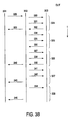
- Fig. 3B is a message diagram showing transactions for data transmission.
- the message diagram illustrates the operation of the system of Fig. 1 for interrupt transactions consisting of OUT transfers. Going top-down the time increases.
- Information exchange between the processor 206 and the bus interface 207 is symbolized by arrows between a first line 301 and a second line 302.
- Information exchange between the bus interface and the second station 203, 204 is symbolized by arrows between the second line 302 and a third line 303.
- the processor 206 needs to transfer data to one of the second stations 203, 204, a USB device.
- the bus interface 207 should repeatedly issue a request to receive data to the bus connections 205. To reduce the communication overhead for the processor 206 it should be sufficient to have the processor 206 provide the request properties only once. If the addressed USB device accepts data, the bus interface 207 should interrupt the processor via the interrupt connection and inform the processor. In case an error occurs the processor 206 should also be notified. In these situations the bus interface 207 should apply an interrupt to the processor 206 too. In other situations no action is required from the processor 206, so that the bus interface 207 should not interrupt the processor 206.
- a OUT transfer 324 the processor in a message 329 sends the request properties to the bus interface 207, where the request properties are stored in the buffer. Based on the request properties within the message 329, which are retrieved from the buffer, the bus interface 207 initiates the OUT transfer by issuing an OUT token 330 on the bus. Subsequently, the bus interface issues a Data packet 331. The second station, the addressed USB device, responds by sending an ACK handshake 332. Upon reception of the ACK handshake 332, the bus interface 207 sends an interrupt signal 333, via the interrupt connection 210, to the processor 206 to inform the processor 206 that the data is transferred successfully. In a different arrangement the bus interface 207 does not send the interrupt signal 332 to the processor 206, since the processor 206 will assume that a successful transmission of the data has occurred if it is not interrupted.
- the bus interface 207 again retrieves the request properties from the buffer 208, while no new information is required from the processor 206.
- the bus interface 207 initiates the OUT transfer by issuing an OUT token 334 on the bus. Subsequently, the bus interface issues a Data packet 335.
- the addressed USB device responds by issuing a NAK handshake 336 to indicate it is not ready to process the transferred data. This completes the OUT transfer 325.
- the bus interface 207 again retrieves the request properties from the buffer 208, while no new information is required from the processor 206.
- the bus interface 207 initiates the OUT transfer by issuing an OUT token 337 on the bus. Subsequently, the bus interface issues a Data packet 338.
- the USB device sends a STALL handshake 339 to indicate it cannot process the OUT transfer.
- the bus interface sends an interrupt signal 340, via the interrupt connection, to the processor 206 to inform the processor on the status of the addressed USB device. This completes the OUT transfer 326.
- the bus interface 207 again retrieves the request properties from the buffer 208, while no new information is required from the processor 206.
- the bus interface 207 initiates the OUT transfer by issuing an OUT token 341 on the bus. Subsequently, the bus interface issues a Data packet 342. Due to an error on the bus, the Data packet 342 is received corrupted by the addressed USB device. For this reason the addressed USB device does not respond.
- the bus interface 207 sends an interrupt signal 343, via the interrupt connection 210, to the processor 206 so as to notify the processor. This completes the OUT transfer 327.
- the bus interface 207 again retrieves the request properties from the buffer 208, while no new information is required from the processor 206.
- the bus interface 207 initiates the OUT transfer by issuing an OUT token 344 on the bus. Due to the occurrence of an error condition the bus interface does not start or complete an already started issuing of a subsequent Data packet. For this reason the bus interface 207 sends an interrupt signal 345 via the interrupt connection 210, to the processor 206 so as to notify the processor. This completes the OUT transfer 328.
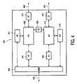
- Fig. 4 is a block diagram showing a bus interface according to the invention.
- the block diagram shown in the figure is a block diagram of a bus interface integrated circuit.
- the bus interface integrated circuit 401 has a dual role. It can be both part of a bus station acting as a USB device and of a bus station acting as a USB host. This is especially useful in a USB On-The-Go (OTG) apparatus.
- OTG On-The-Go
- Such a USB OTG apparatus could be, for example, a digital still camera, a digital video camera, a personal digital assistant, or an oscilloscope, which in a certain mode of operation is connected, via USB, for example, to a mass storage apparatus (e.g.
- USB OTG apparatus In this mode of operation the USB OTG apparatus should act as a USB host. In another mode of operation the USB OTG is connected, via USB, for example, to a personal computer. In this mode of operation the USB OTG apparatus should act as a USB device.
- the mode in which the bus interface integrated circuit of the USB OTG apparatus operates could be software determined and controlled by a processor within the USB OTG apparatus.
- USB OTG apparatus In case the USB OTG apparatus is portable it could be advantageous to include a low power consumption mode available in which the bus interface integrated circuits shuts down certain functional blocks or operates at a lower clock speed in time periods with, for example low bus traffic or no bus traffic at all.
- a low power consumption mode could be enhanced by including a so-called remote wake-up feature, controlled by the processor of the USB OTG apparatus, to bring back to operation certain or all functional blocks or to increase the clock speed of the bus interface integrated circuit.
- the remote wake-up feature could be activated, for example, if the processor anticipates increased bus traffic.
- the bus interface integrated circuit 401 comprises a connection 402 with an processor, a connection 403 for connection to a USB in case the bus interface integrated circuit 401 operates as a USB host, and a connection 404 for connection to a USB in case the bus interface integrated circuit 401 operates as a USB device.
- connections 403 and 404 could share the same I/O terminals, while an internal multiplexer takes care of the internal routing of the bus signals. Such an implementation could be advantageous in case it is guaranteed that connections 403 are not used simultaneously.
- the bus interface integrated circuit 401 also comprises a host-device multiplexer 405, a timing block 406, a host interface 407, a device interface 408, a host controller 409, a device controller 410, a host buffer 411, a device buffer 412, a host transceiver 413, and a device transceiver 414.
- the host-device multiplexer 405 is connected to the connection 402 with the processor. Preferably under the control of the processor it determines the internal routing of the communication of the bus interface integrated circuit 401 with the processor. In case the bus interface integrated circuit 401 operates as a USB host, the host-device multiplexer 405 links the host controller 409, via the host interface 407, to the processor. In case the bus interface integrated circuit 401 operates as a USB device, the host-device multiplexer links the device controller 410, via the device interface 408, to the processor. The host controller 409 has access to the bus connection 403 via the host transceiver 413. The device controller 410 has access to the bus connection 404 via the device transceiver 414.
- the host buffer 411 is accessible by both the host controller 409 and, via the host-device multiplexer 405, by the processor. It can be used, for example, for storing request properties issued by the processor and for storing results of the communication between the host controller 411 and a USB device.
- the device buffer 412 is accessible by both the device controller 410 and via the host-device multiplexer 405, by the processor. It can be used, for example, for buffering data generated by the processor, so as to be sent to a USB host.
- the host buffer 411 and the device buffer 412 are preferably accessible by the processor in both a direct memory access (DMA) mode and a parallel input-output mode.
- DMA direct memory access
- the bus interface As an integrated circuit.
- the functional integration in an integrated circuit enables a reduction in component count and area minimization and hence will result in a reduction in physical size of a bus station comprising the bus interface.
- realizing the bus interface as an integrated circuit will allow for a reduction in power consumption.
- bus interface Depending on the requirements of the bus system, it is advantageous to realize the bus interface with a plurality of integrated circuits and discrete electronic components, utilizing as much as possible standard building blocks. This reduces the cost price of the bus interface.
- Fig. 5 is schematic overview of a buffer 501 organized in a first-in, first-out (FIFO) manner. This in an efficient manner to organize the host buffer 411.
- the top of the FIFO buffer is indicated by an arrow 502.
- the bottom of the FIFO buffer is indicated by an arrow 503.
- the buffer stores request properties of several requests 504, 505, 506, for example, for initiating USB transactions or more in particular USB interrupt transactions.
- the request properties first issued are indicated by 504
- the request properties issued second are indicated by 505
- the request properties issued last are indicated by 506.
- the area 507 indicates the remaining request properties, while the area 508 indicates the remaining space in the FIFO buffer not being used.
- Request properties are divided in two parts: a transfer descriptor or header 509 and, if applicable, payload data 510.
- the transfer descriptor 509 describes the characteristics of the transaction to be handled by the host controller 409.
- the payload data 510 is the data that should be included in the Data packet of the transaction to be handled by the host controller.
- the transfer descriptor is also used by the host controller 409 to store the results of transactions. Therefore, both the processor and the host controller 409 have access to the FIFO buffer 501.
- the buffer in a first-in first-out mode. In this way it is relatively simple to access the data stored in the buffer for both the processor as the controller.
- the buffer it is advantageous to use the buffer to store both request properties and the results of the communication with the second station.
- the processor By giving the processor read access to the buffer, or at least designated sections of the buffer, an efficient way of communication is established, since the same buffer is used to store the request properties and the results of the requests.
- the processor can access the buffer in an identical way as when it writes the request properties, only the type of access has to changed from a write mode to a read mode.
- the bus interface determines the exact polling interval based on information provided by the processor. Limiting the number of possible polling rates simplifies the task of the bus interface in handling different requests with different polling rates. For example, if the processor may choose any polling rate between 1, 2, 3, and 128 milliseconds, the bus interface maps the chosen polling rate to one of the following actual polling rates: 1, 2, 4, 8, 16, 32, 64, or 128 milliseconds, thus reducing the potential number of different polling rates to handle from 128 to 8. Preferably, the bus interface maps the polling rate chosen by the processor on the actual polling rate that is closest to the chosen polling rate.
- the table below shows a format of the transfer descriptor.
- the format shown consists of 8 bytes, indicated as Byte 0, Byte 1, ..., Byte 7. Every byte consists of 8 bits, enumerated as 0, 1, ..., 7. - 7 6 5 4 3 2 1 0 Byte 0 Actual bytes (7:0) Byte 1 Completion code Active Toggle Actual bytes (9:8) Byte 2 MaxPktSize (7:0) Byte 3 Endpoint number (3:0) Last Speed MaxPktSize (9:8) Byte 4 Total bytes (7:0) Byte 5 0 0 Res Res Dir. token (1:0) Total bytes (9:8) Byte 6 0 Device address Byte 7 Interrupt polling interval (4:0)
Landscapes
- Engineering & Computer Science (AREA)
- Theoretical Computer Science (AREA)
- Physics & Mathematics (AREA)
- General Engineering & Computer Science (AREA)
- General Physics & Mathematics (AREA)
- Information Transfer Systems (AREA)
- Small-Scale Networks (AREA)
- Traffic Control Systems (AREA)
- Organic Insulating Materials (AREA)
- Fixing For Electrophotography (AREA)
Claims (8)
- Bus-System, das eine erste Station (202) und eine zweite Station (203, 204) umfasst, die durch einen Bus zum Übertragen von Daten- und Steuersignalen gekoppelt sind, wobei der Bus dafür ausgelegt ist, entsprechend einem Protokoll zu arbeiten, in welchem die erste Station (202) wiederholt Anfragen zu der zweiten Station (203, 204) sendet, wobei die erste Station (202) einen Prozessor (206), eine Bus-Schnittstelle (207) und einen mit dem Prozessor (206) und der Bus-Schnittstelle (207) gekoppelten Puffer (208) umfasst, wobei
der Prozessor (206) so betreibbar ist, dass er Anfrageeigenschaften für die Anfragen und für das Handhaben der Daten- und Steuersignale erzeugt;
der Puffer (208) so betreibbar ist, dass er die Anfrageeigenschaften speichert; und
die Bus-Schnittstelle (207) so betreibbar ist, dass sie die Anfragen aus den gespeicherten Anfrageeigenschaften erzeugt und die Anfragen wiederholt sendet;
dadurch gekennzeichnet, dass die Anfrageeigenschaften eine Abrufrate der Anfragen umfassen. - Bus-System nach Anspruch 1, dadurch gekennzeichnet, dass die Anfrageeigenschaften ferner eine Nutzlast der Anfragen umfassen.
- Bus-System nach Anspruch 1, dadurch gekennzeichnet, dass die zweite Station (203, 204) auf die Anfragen antwortet, dass der Prozessor (206) ein unterbrechbarer Prozessor ist, und dass die Bus-Schnittstelle (207) so betreibbar ist, dass sie den Prozessor (206) bei Empfang von ausgewählten Antworten der zweiten Station (203, 204) unterbricht.
- Bus-System nach Anspruch 1, dadurch gekennzeichnet, dass das Bus-System ein USB-System ist.
- Bus-Schnittstelle zur Verwendung in einer ersten Station eines Bus-Systems, das die erste Station (202) und eine zweite Station (203, 204) umfasst, die durch einen Bus zum Übertragen von Daten- und Steuersignalen gekoppelt sind, wobei der Bus dafür ausgelegt ist, entsprechend einem Protokoll zu arbeiten, in welchem die erste Station (202) wiederholt Anfragen zu der zweiten Station (203, 204) sendet, eine Verbindung (403) für den Bus und einen Eingang zum Empfangen von Anfrageeigenschaften von einem Prozessor umfassend, wobei die Bus-Schnittstelle einen Puffer (411), der so betreibbar ist, dass er die Anfrageeigenschaften speichert, sowie eine Steuervorrichtung (409) umfasst, die so betreibbar ist, dass sie Anfragen aus den gespeicherten Anfrageeigenschaften erzeugt und die Anfragen wiederholt zu der Verbindung (403) sendet;
dadurch gekennzeichnet, dass die Anfrageeigenschaften eine Abrufrate der Anfragen umfassen. - Bus-Schnittstelle nach Anspruch 5, dadurch gekennzeichnet, dass die Anfrageeigenschaften ferner eine Nutzlast der Anfragen umfassen.
- Bus-Schnittstelle nach Anspruch 5, dadurch gekennzeichnet, dass die Bus-Schnittstelle ferner einen Unterbrechungsausgang zum Senden eines Unterbrechungssignals zu einem unterbrechbaren Prozessor umfasst, und dass die Steuervorrichtung (409) so betreibbar ist, dass sie Antworten von der Verbindung empfängt und den Prozessor bei Empfang ausgewählter Antworten unterbricht, indem sie ein Unterbrechungssignal zu dem Unterbrechungsausgang sendet.
- Bus-Schnittstelle nach Anspruch 5, dadurch gekennzeichnet, dass die Bus-Schnittstelle so betreibbar ist, dass sie als USB-Schnittstelle arbeitet.
Applications Claiming Priority (3)
| Application Number | Priority Date | Filing Date | Title |
|---|---|---|---|
| SG0100194 | 2001-09-27 | ||
| WOPCT/SG01/00194 | 2001-09-27 | ||
| PCT/IB2002/003812 WO2003029996A1 (en) | 2001-09-27 | 2002-09-16 | Bus system and bus interface for connection to a bus |
Publications (2)
| Publication Number | Publication Date |
|---|---|
| EP1433069A1 EP1433069A1 (de) | 2004-06-30 |
| EP1433069B1 true EP1433069B1 (de) | 2010-11-10 |
Family
ID=20428993
Family Applications (1)
| Application Number | Title | Priority Date | Filing Date |
|---|---|---|---|
| EP02765263A Expired - Lifetime EP1433069B1 (de) | 2001-09-27 | 2002-09-16 | Bussytem und busschnittstelle zum anschliessen an einen bus |
Country Status (9)
| Country | Link |
|---|---|
| US (1) | US7058747B2 (de) |
| EP (1) | EP1433069B1 (de) |
| JP (1) | JP2005504392A (de) |
| KR (1) | KR20040041623A (de) |
| CN (1) | CN100351824C (de) |
| AT (1) | ATE487986T1 (de) |
| DE (1) | DE60238264D1 (de) |
| TW (1) | TWI233553B (de) |
| WO (1) | WO2003029996A1 (de) |
Families Citing this family (14)
| Publication number | Priority date | Publication date | Assignee | Title |
|---|---|---|---|---|
| US7000057B1 (en) * | 2002-02-11 | 2006-02-14 | Cypress Semiconductor Corp. | Method and apparatus for adding OTG dual role device capability to a USB peripheral |
| US7752342B2 (en) * | 2002-09-24 | 2010-07-06 | Nxp B.V. | Interface integrated circuit device for a USB connection |
| ATE369587T1 (de) | 2003-05-15 | 2007-08-15 | Nxp Bv | Usb host controller mit speicher für transferdeskriptoren |
| JP3649227B2 (ja) * | 2003-06-06 | 2005-05-18 | セイコーエプソン株式会社 | データ転送制御装置、電子機器及びデータ転送制御方法 |
| GB0327216D0 (en) * | 2003-11-22 | 2003-12-24 | Nokia Corp | An interface for serial data communication |
| US20060123179A1 (en) * | 2004-12-03 | 2006-06-08 | Wong Kar L | Controlling issuance of requests |
| US7610416B2 (en) * | 2005-04-13 | 2009-10-27 | Microsoft Corporation | Systems and methods for controlling rise and fall times of USB signals |
| US7409485B1 (en) * | 2005-10-27 | 2008-08-05 | Cisco Technology, Inc. | Optimized data transfer for a data bus |
| US9619004B1 (en) * | 2006-12-20 | 2017-04-11 | Nvidia Corporation | Reducing system power consumption due to USB host controllers |
| US8473647B2 (en) * | 2007-09-17 | 2013-06-25 | Apple Inc. | Methods and apparatus for decreasing power consumption and bus activity |
| CN101266584B (zh) * | 2008-05-13 | 2011-05-11 | 威盛电子股份有限公司 | 通用串行总线主机控制器及其控制方法 |
| US9087163B2 (en) * | 2012-07-11 | 2015-07-21 | Silicon Image, Inc. | Transmission of multiple protocol data elements via an interface utilizing a data tunnel |
| CN105630722B (zh) * | 2015-12-21 | 2019-03-08 | 联想(北京)有限公司 | 电子设备及信号处理方法 |
| CN105573946B (zh) * | 2016-03-01 | 2019-03-01 | Oppo广东移动通信有限公司 | 通用串行总线接口复用的方法及装置 |
Family Cites Families (10)
| Publication number | Priority date | Publication date | Assignee | Title |
|---|---|---|---|---|
| JPS60126945A (ja) * | 1983-12-14 | 1985-07-06 | Hitachi Ltd | ポ−リング方式 |
| JPH0771094B2 (ja) * | 1989-05-19 | 1995-07-31 | オムロン株式会社 | 通信ネットワークシステム |
| US5675807A (en) * | 1992-12-17 | 1997-10-07 | Tandem Computers Incorporated | Interrupt message delivery identified by storage location of received interrupt data |
| EP0652523B1 (de) * | 1993-11-10 | 1999-06-02 | Nec Corporation | Fernüberwachungssystem |
| US5974486A (en) * | 1997-08-12 | 1999-10-26 | Atmel Corporation | Universal serial bus device controller comprising a FIFO associated with a plurality of endpoints and a memory for storing an identifier of a current endpoint |
| US6058440A (en) * | 1997-09-05 | 2000-05-02 | Intel Corporation | Programmable and adaptive resource allocation device and resource use recorder |
| US6145045A (en) * | 1998-01-07 | 2000-11-07 | National Semiconductor Corporation | System for sending and receiving data on a Universal Serial Bus (USB) using a memory shared among a number of end points |
| CN1273903C (zh) * | 1998-03-19 | 2006-09-06 | 韩旭 | 通用串行总线多功能转接控制器 |
| US6449663B1 (en) * | 1998-07-08 | 2002-09-10 | International Business Machines Corporation | Method and apparatus for adjusting an interval of polling a network printer based on changes in working status of the network printer |
| US6640268B1 (en) * | 1998-08-28 | 2003-10-28 | Intel Corporation | Dynamic polling mechanism for wireless devices |
-
2002
- 2002-09-16 AT AT02765263T patent/ATE487986T1/de not_active IP Right Cessation
- 2002-09-16 JP JP2003533133A patent/JP2005504392A/ja active Pending
- 2002-09-16 EP EP02765263A patent/EP1433069B1/de not_active Expired - Lifetime
- 2002-09-16 CN CNB028190009A patent/CN100351824C/zh not_active Expired - Fee Related
- 2002-09-16 WO PCT/IB2002/003812 patent/WO2003029996A1/en not_active Ceased
- 2002-09-16 DE DE60238264T patent/DE60238264D1/de not_active Expired - Lifetime
- 2002-09-16 KR KR10-2004-7004352A patent/KR20040041623A/ko not_active Ceased
- 2002-09-19 TW TW091121489A patent/TWI233553B/zh not_active IP Right Cessation
- 2002-09-24 US US10/253,284 patent/US7058747B2/en not_active Expired - Lifetime
Also Published As
| Publication number | Publication date |
|---|---|
| CN1559039A (zh) | 2004-12-29 |
| US20030101308A1 (en) | 2003-05-29 |
| TWI233553B (en) | 2005-06-01 |
| CN100351824C (zh) | 2007-11-28 |
| WO2003029996A1 (en) | 2003-04-10 |
| JP2005504392A (ja) | 2005-02-10 |
| KR20040041623A (ko) | 2004-05-17 |
| DE60238264D1 (de) | 2010-12-23 |
| EP1433069A1 (de) | 2004-06-30 |
| US7058747B2 (en) | 2006-06-06 |
| ATE487986T1 (de) | 2010-11-15 |
Similar Documents
| Publication | Publication Date | Title |
|---|---|---|
| US7577773B1 (en) | Method and system for DMA optimization | |
| US6070214A (en) | Serially linked bus bridge for expanding access over a first bus to a second bus | |
| US6219736B1 (en) | Universal serial bus (USB) RAM architecture for use with microcomputers via an interface optimized for integrated services device network (ISDN) | |
| US6088752A (en) | Method and apparatus for exchanging information between buses in a portable computer and docking station through a bridge employing a serial link | |
| EP1433071B1 (de) | Bussystem und busschnittstelle zur verbindung mit einem bus | |
| US6898751B2 (en) | Method and system for optimizing polling in systems using negative acknowledgement protocols | |
| EP1433069B1 (de) | Bussytem und busschnittstelle zum anschliessen an einen bus | |
| US7043589B2 (en) | Bus system and bus interface | |
| CN120153367A (zh) | 快速外围组件互连设备之间的流控制 | |
| JP2005122372A (ja) | データ転送制御装置、電子機器及びデータ転送制御方法 | |
| JP2003316729A (ja) | データ転送制御装置、電子機器及びデータ転送制御方法 | |
| US20070245059A1 (en) | Bus Connection Device | |
| US20070022226A1 (en) | Direct memory access system for iSCSI | |
| AU751826B2 (en) | Linked Bridge | |
| CA2347896C (en) | Docking system and method | |
| EP1653373B1 (de) | Busbrücke |
Legal Events
| Date | Code | Title | Description |
|---|---|---|---|
| PUAI | Public reference made under article 153(3) epc to a published international application that has entered the european phase |
Free format text: ORIGINAL CODE: 0009012 |
|
| 17P | Request for examination filed |
Effective date: 20040427 |
|
| AK | Designated contracting states |
Kind code of ref document: A1 Designated state(s): AT BE BG CH CY CZ DE DK EE ES FI FR GB GR IE IT LI LU MC NL PT SE SK TR |
|
| RAP1 | Party data changed (applicant data changed or rights of an application transferred) |
Owner name: NXP B.V. |
|
| GRAP | Despatch of communication of intention to grant a patent |
Free format text: ORIGINAL CODE: EPIDOSNIGR1 |
|
| GRAS | Grant fee paid |
Free format text: ORIGINAL CODE: EPIDOSNIGR3 |
|
| GRAA | (expected) grant |
Free format text: ORIGINAL CODE: 0009210 |
|
| AK | Designated contracting states |
Kind code of ref document: B1 Designated state(s): AT BE BG CH CY CZ DE DK EE ES FI FR GB GR IE IT LI LU MC NL PT SE SK TR |
|
| REG | Reference to a national code |
Ref country code: GB Ref legal event code: FG4D |
|
| REG | Reference to a national code |
Ref country code: CH Ref legal event code: EP |
|
| REG | Reference to a national code |
Ref country code: IE Ref legal event code: FG4D |
|
| REF | Corresponds to: |
Ref document number: 60238264 Country of ref document: DE Date of ref document: 20101223 Kind code of ref document: P |
|
| REG | Reference to a national code |
Ref country code: GB Ref legal event code: 732E Free format text: REGISTERED BETWEEN 20110120 AND 20110126 |
|
| REG | Reference to a national code |
Ref country code: NL Ref legal event code: VDEP Effective date: 20101110 |
|
| PG25 | Lapsed in a contracting state [announced via postgrant information from national office to epo] |
Ref country code: PT Free format text: LAPSE BECAUSE OF FAILURE TO SUBMIT A TRANSLATION OF THE DESCRIPTION OR TO PAY THE FEE WITHIN THE PRESCRIBED TIME-LIMIT Effective date: 20110310 Ref country code: NL Free format text: LAPSE BECAUSE OF FAILURE TO SUBMIT A TRANSLATION OF THE DESCRIPTION OR TO PAY THE FEE WITHIN THE PRESCRIBED TIME-LIMIT Effective date: 20101110 Ref country code: CY Free format text: LAPSE BECAUSE OF FAILURE TO SUBMIT A TRANSLATION OF THE DESCRIPTION OR TO PAY THE FEE WITHIN THE PRESCRIBED TIME-LIMIT Effective date: 20101110 Ref country code: FI Free format text: LAPSE BECAUSE OF FAILURE TO SUBMIT A TRANSLATION OF THE DESCRIPTION OR TO PAY THE FEE WITHIN THE PRESCRIBED TIME-LIMIT Effective date: 20101110 Ref country code: AT Free format text: LAPSE BECAUSE OF FAILURE TO SUBMIT A TRANSLATION OF THE DESCRIPTION OR TO PAY THE FEE WITHIN THE PRESCRIBED TIME-LIMIT Effective date: 20101110 Ref country code: SE Free format text: LAPSE BECAUSE OF FAILURE TO SUBMIT A TRANSLATION OF THE DESCRIPTION OR TO PAY THE FEE WITHIN THE PRESCRIBED TIME-LIMIT Effective date: 20101110 Ref country code: BG Free format text: LAPSE BECAUSE OF FAILURE TO SUBMIT A TRANSLATION OF THE DESCRIPTION OR TO PAY THE FEE WITHIN THE PRESCRIBED TIME-LIMIT Effective date: 20110210 |
|
| PG25 | Lapsed in a contracting state [announced via postgrant information from national office to epo] |
Ref country code: GR Free format text: LAPSE BECAUSE OF FAILURE TO SUBMIT A TRANSLATION OF THE DESCRIPTION OR TO PAY THE FEE WITHIN THE PRESCRIBED TIME-LIMIT Effective date: 20110211 |
|
| PG25 | Lapsed in a contracting state [announced via postgrant information from national office to epo] |
Ref country code: BE Free format text: LAPSE BECAUSE OF FAILURE TO SUBMIT A TRANSLATION OF THE DESCRIPTION OR TO PAY THE FEE WITHIN THE PRESCRIBED TIME-LIMIT Effective date: 20101110 Ref country code: ES Free format text: LAPSE BECAUSE OF FAILURE TO SUBMIT A TRANSLATION OF THE DESCRIPTION OR TO PAY THE FEE WITHIN THE PRESCRIBED TIME-LIMIT Effective date: 20110221 Ref country code: CZ Free format text: LAPSE BECAUSE OF FAILURE TO SUBMIT A TRANSLATION OF THE DESCRIPTION OR TO PAY THE FEE WITHIN THE PRESCRIBED TIME-LIMIT Effective date: 20101110 Ref country code: EE Free format text: LAPSE BECAUSE OF FAILURE TO SUBMIT A TRANSLATION OF THE DESCRIPTION OR TO PAY THE FEE WITHIN THE PRESCRIBED TIME-LIMIT Effective date: 20101110 |
|
| PG25 | Lapsed in a contracting state [announced via postgrant information from national office to epo] |
Ref country code: DK Free format text: LAPSE BECAUSE OF FAILURE TO SUBMIT A TRANSLATION OF THE DESCRIPTION OR TO PAY THE FEE WITHIN THE PRESCRIBED TIME-LIMIT Effective date: 20101110 Ref country code: SK Free format text: LAPSE BECAUSE OF FAILURE TO SUBMIT A TRANSLATION OF THE DESCRIPTION OR TO PAY THE FEE WITHIN THE PRESCRIBED TIME-LIMIT Effective date: 20101110 |
|
| PLBE | No opposition filed within time limit |
Free format text: ORIGINAL CODE: 0009261 |
|
| STAA | Information on the status of an ep patent application or granted ep patent |
Free format text: STATUS: NO OPPOSITION FILED WITHIN TIME LIMIT |
|
| 26N | No opposition filed |
Effective date: 20110811 |
|
| REG | Reference to a national code |
Ref country code: DE Ref legal event code: R097 Ref document number: 60238264 Country of ref document: DE Effective date: 20110811 |
|
| PG25 | Lapsed in a contracting state [announced via postgrant information from national office to epo] |
Ref country code: IT Free format text: LAPSE BECAUSE OF FAILURE TO SUBMIT A TRANSLATION OF THE DESCRIPTION OR TO PAY THE FEE WITHIN THE PRESCRIBED TIME-LIMIT Effective date: 20101110 |
|
| PG25 | Lapsed in a contracting state [announced via postgrant information from national office to epo] |
Ref country code: MC Free format text: LAPSE BECAUSE OF NON-PAYMENT OF DUE FEES Effective date: 20110930 |
|
| REG | Reference to a national code |
Ref country code: CH Ref legal event code: PL |
|
| REG | Reference to a national code |
Ref country code: IE Ref legal event code: MM4A |
|
| REG | Reference to a national code |
Ref country code: FR Ref legal event code: ST Effective date: 20120531 |
|
| PG25 | Lapsed in a contracting state [announced via postgrant information from national office to epo] |
Ref country code: LI Free format text: LAPSE BECAUSE OF NON-PAYMENT OF DUE FEES Effective date: 20110930 Ref country code: CH Free format text: LAPSE BECAUSE OF NON-PAYMENT OF DUE FEES Effective date: 20110930 Ref country code: IE Free format text: LAPSE BECAUSE OF NON-PAYMENT OF DUE FEES Effective date: 20110916 |
|
| PG25 | Lapsed in a contracting state [announced via postgrant information from national office to epo] |
Ref country code: FR Free format text: LAPSE BECAUSE OF NON-PAYMENT OF DUE FEES Effective date: 20110930 |
|
| PG25 | Lapsed in a contracting state [announced via postgrant information from national office to epo] |
Ref country code: LU Free format text: LAPSE BECAUSE OF NON-PAYMENT OF DUE FEES Effective date: 20110916 |
|
| PG25 | Lapsed in a contracting state [announced via postgrant information from national office to epo] |
Ref country code: TR Free format text: LAPSE BECAUSE OF FAILURE TO SUBMIT A TRANSLATION OF THE DESCRIPTION OR TO PAY THE FEE WITHIN THE PRESCRIBED TIME-LIMIT Effective date: 20101110 |
|
| REG | Reference to a national code |
Ref country code: DE Ref legal event code: R082 Ref document number: 60238264 Country of ref document: DE Representative=s name: GRUENECKER PATENT- UND RECHTSANWAELTE PARTG MB, DE Ref country code: DE Ref legal event code: R081 Ref document number: 60238264 Country of ref document: DE Owner name: OCT CIRCUIT TECHNOLOGIES INTERNATIONAL LTD., IE Free format text: FORMER OWNER: NXP B.V., EINDHOVEN, NL |
|
| PGFP | Annual fee paid to national office [announced via postgrant information from national office to epo] |
Ref country code: GB Payment date: 20170821 Year of fee payment: 16 Ref country code: DE Payment date: 20170821 Year of fee payment: 16 |
|
| REG | Reference to a national code |
Ref country code: DE Ref legal event code: R119 Ref document number: 60238264 Country of ref document: DE |
|
| GBPC | Gb: european patent ceased through non-payment of renewal fee |
Effective date: 20180916 |
|
| PG25 | Lapsed in a contracting state [announced via postgrant information from national office to epo] |
Ref country code: DE Free format text: LAPSE BECAUSE OF NON-PAYMENT OF DUE FEES Effective date: 20190402 |
|
| PG25 | Lapsed in a contracting state [announced via postgrant information from national office to epo] |
Ref country code: GB Free format text: LAPSE BECAUSE OF NON-PAYMENT OF DUE FEES Effective date: 20180916 |